
A 280 GHz 30 GHz Bandwidth Cascaded Amplifier Using Flexible Interstage Matching Strategy in 130 nm SiGe Technology


Division of Electronics and Electrical Engineering, Dongguk University, Seoul 04620, Korea
*
Author to whom correspondence should be addressed.
Electronics 2022, 11(19), 3045; https://doi.org/10.3390/electronics11193045
Submission received: 30 August 2022
/
Revised: 19 September 2022
/
Accepted: 21 September 2022
/
Published: 24 September 2022
(This article belongs to the Special Issue Microwave/Millimeter-Wave Power Amplifiers)
Abstract
:This paper presents a 280 GHz amplifier design strategy for a robust multistage amplifier in a sub-Terahertz (sub-THz) regime in 130 nm SiGe technology. The presented 280 GHz amplifier consists of 14 stages of the cascaded common emitter (CE) amplifier which offers a compact and improved-noise design due to the absence of the area-expensive and lossy baluns at such high frequencies. The interstage-matching network was flexibly constructed with two separate resonant tanks using metal–insulator–metal (MIM) capacitors and microstrip transmission lines (MSTLs) between each stage. The measured amplifier achieved a peak power gain of 10.9 dB at 283 GHz and a 3 dB gain of bandwidth of 30 GHz between 270 and 300 GHz. The peak output power of the amplifier was 0.8 dBm with an output of 1 dB gain compression point (OP1dB) of −3.6 dBm in simulation. The 14-stage amplifier consumes an area of 0.213 mm2, including all the pads. With the proposed interstage matching approach, a well-balanced 280 GHz amplifier has been demonstrated. The proposed design strategy is widely applicable to sub-THz receivers for future wireless communication systems.
1. Introduction
Sub-terahertz (sub-THz) frequencies are highly potential to be used in many applications such as sensing and wireless communication at close distances [1]. Shorter wavelengths could improve an imaging system’s resolution. Due to the unique absorption spectra of various materials in the sub-THz and THz bands, spectroscopy at these bands is also employed in agriculture and food products, the detection of concealed or dangerous objects, cancer scanning, etc. [2,3,4]. In addition, wireless systems can achieve up to hundreds of Gbps of bandwidth by shifting to sub-THz frequencies. Sub-terahertz transceivers have demonstrated an explosive increase in data rate and delay compared to 5G networks, opening the door to a 6G network. The first attempts at standardization of sub-terahertz band wireless connections were found in [5]. Data centers, device-to-device connections, and front-haul and back-haul mobile networks could benefit from short-range wireless links. Moreover, the potential high-speed availability of these systems could be applicable in several applications such as robotic control, autonomous vehicles, or information showers [6]. Recently indoor network with a sub-terahertz band wireless link has been proposed for 6G applications [7].
As the cut-off frequency (fT) and the maximum frequency of oscillation (fmax) of the silicon-based transistors continue to improve, silicon-based technologies are seriously considered suitable for designing fully integrated sub-THz transceivers that can significantly reduce cost, effort, and time to market. Recent demonstrations of sub-terahertz technology have included complete transceivers for communication links [8,9,10,11,12,13,14,15], single transmitters [16,17], and receiver designs [18,19,20,21]. Using push–pull subharmonic mixer architecture, a 300 GHz CMOS transceiver could reach 34 Gb/s of data transmissions [8]. Specifically, wireless communication links using SiGe technologies were demonstrated to reach data rates up to 100 Gb/s [9,10,11,12].
At such high frequencies, signal amplification becomes an important task to improve system performance. Although the mixer-first receivers are still quite prevalent at sub-THz bands, the use of low-noise amplifiers (LNAs) has gained increasing attention recently owing to the improved RF performance (fT/fmax) of the advanced SiGe technologies. In the transmitter, a power amplifier (PA) is necessary to amplify the transmitted signal power to enlarge the communication distance. In addition, stronger drivers in the local oscillator (LO) chain are also necessary to improve the mixers’ noise performance, conversion gain, and linearity. Recently, in the 300 GHz band, there have been noticeable efforts to develop silicon-based low-noise amplifiers (LNAs) or drivers [22,23,24,25,26,27]. By employing an inductive feedback network, each common source (CS) amplifying stage could boost its gain close to the maximum achievable gain available by the CMOS process. Applying this technique, the work in [22] attained a power gain of 21 dB with 16 stages of CS amplifier, in a trade-off with a significantly reduced operation bandwidth which was nearly 1 GHz in the measurement. A similar CMOS amplifier using inductive feedback attains a power gain of 12 dB with only three amplifying stages and an estimated bandwidth of merely around 10 GHz [23]. A differential cascade structure with optimum impedance matching can maximize the gain of the amplifying stage at the cost of a relatively large area consumption and additional baluns required at the input and output. Using this strategy, a three-stage 300 GHz LNA with 10.8 dB gain and 68 GHz bandwidth has been presented in an advanced 130 nm SiGe technology with fT/fmax of 470/700 GHz [24]. Other similar designs could be found in [25,26,27] where the reported performances were achieved with trade-offs between gain, bandwidth, and area occupancy.
This work presents a 280GHz amplifier using a 130 nm SiGe technology which nominally offers fT/fmax of 350/450 GHz. The designed amplifier was optimized for multi-purpose applications such as a low-noise amplifier and driving amplifier as well. It should be noted that the optimal noise and gain source impedances approach each other since the equivalent noise resistance (Rn) becomes smaller as the working frequency approaches the cut-off frequency for a conventional MOS device [28], and it is applicable to HBT as well. This multi-purpose amplifier requires low noise performance, large bandwidth, compact area, and low DC power consumption. Hence, the design approaches used in this amplifier are suitable for transceivers in the future, sub-THz wireless communication systems that characterize broad bandwidths for high data-rate transmission. For this objective, the single-ended CE amplifying structure was co-designed with a compact impedance matching network for improved noise performance with reduced insertion-loss and area occupancy. Moreover, eliminating the baluns at the two terminals saves area and further enhances the noise figure due to the significant loss of the sub-THz baluns. A flexible interstage impedance matching approach was employed to improve the bandwidth and area occupation. With the presented approach, a wider bandwidth with more amplifying stages could be possible. The designed 14-stage amplifier occupied an area of 0.7 × 0.3 mm2 and consumed a dc-power of 99.2 mW. The measured power gain was 10.9 dB at the center frequency of 283 GHz with a 3 dB gain bandwidth of 30 GHz between 270 and 300 GHz. In the following, the amplifier design is described in Section 2, the simulation and measurement results are presented in Section 3, and they are followed by a conclusion in Section 4.
2. 280-GHz Cascaded Amplifier Design
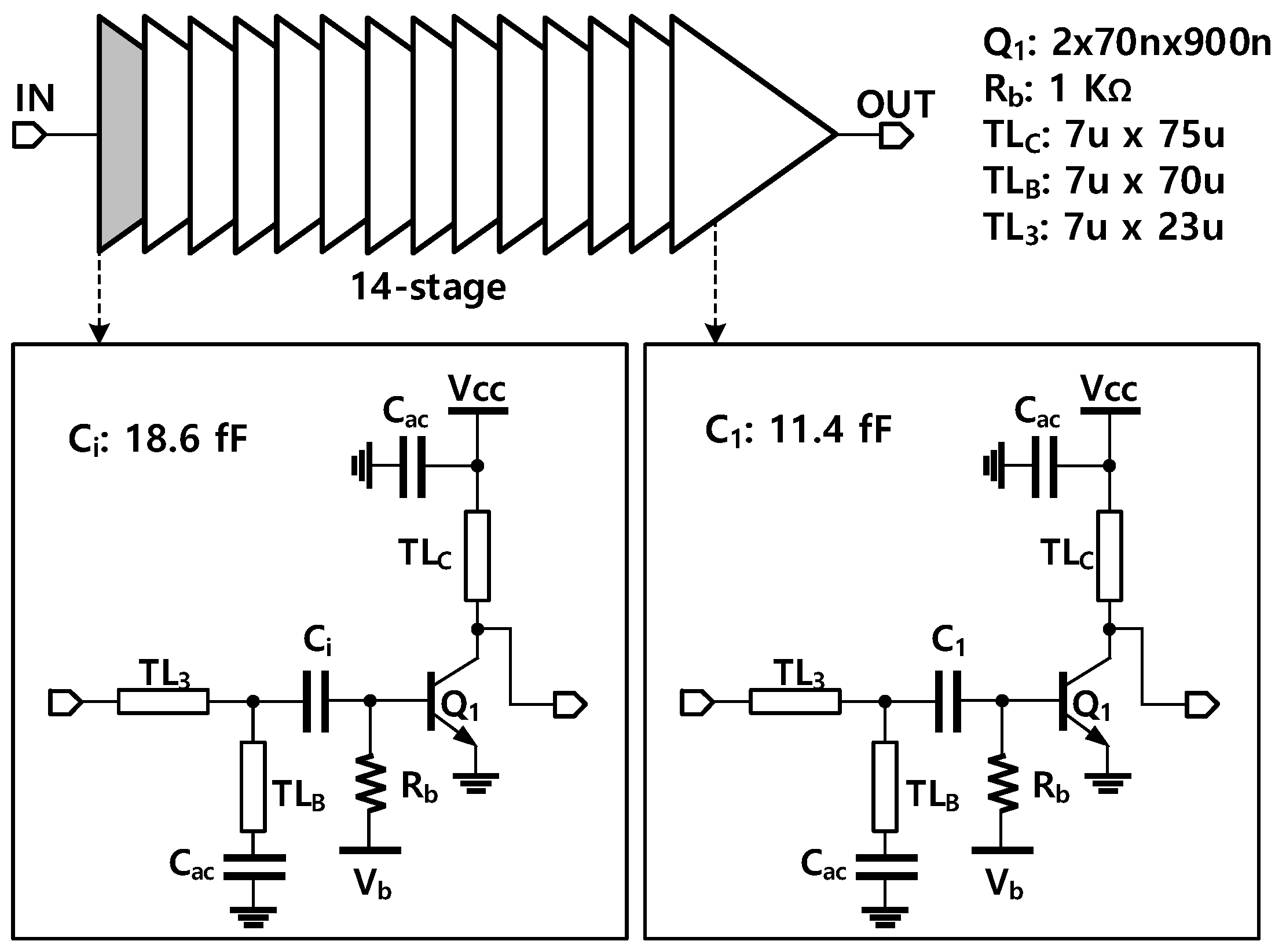
The schematic of the 280 GHz amplifier is presented in Figure 1. Since the simulated fmax of the post-layout extracted HBT of the used SiGe technology is around 420 GHz, it is feasible to attain power gain at 280 GHz. Aiming at a gain higher than 10 dB at the target frequency, the implemented amplifier consists of 14 stages of a common emitter (CE) amplifier considering the large loss in the matching networks. The interstage-matching network should be carefully designed considering loss, bandwidth, and compact layout. For a cascaded RF amplifier with n number of the identical amplifier having a 2nd order RLC tank with a quality factor Qs, = f0/BWs, the bandwidth of the cascaded amplifier (BWn-cas) can be expressed as
For a single-stage amplifier having a tank with Q = 2 (BWS = 150 GHz and f0 = 300 GHz), the bandwidth of the cascaded amplifier with 14 stages was reduced to 33.8 GHz. In each stage, a single-ended CE configuration was used. Hence, baluns for the input and output ports were unnecessary. In this way, the attained gain of the amplifier could be saved by more than 2 dB compared with the differential amplifier with Marchand baluns at 300 GHz. The impedance matching network was constructed from two transmission lines (T-line), and a metal–insulator–metal (MIM) capacitor was used to perform impedance matchings for the active device at each stage. The device size was chosen to be 2 × 70 nm × 900 nm so that the T-line-based stubs are long enough for a clear path modeling for EM simulation. Because the base resistance is around four times lower than the collector resistance, the series capacitors were used to transform the low impedance of the base to match the high impedance of the collector.
2.1. Device Selection and Bias Design
When designing an amplifier, the first step is to select a proper bias for the active device since the optimal bias is relatively independent of the active device size and the matching network. For a sub-THz driving amplifier, the bias value should be chosen for the highest available gain. If the active device is in the output stage of a power amplifier, the bias value should be selected based on the output power criteria and the linearity. This work aimed to design a driving amplifier that can be used as a low-noise amplifier or a buffer stage in the local oscillator (LO) path. Therefore, the bias selection for the base of a transistor was optimized for the gain of the active device.
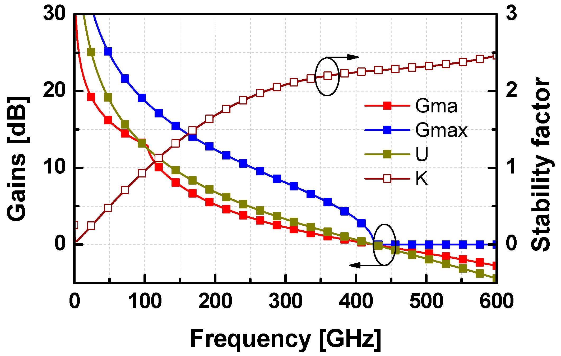
We performed an s-parameter simulation on a post-layout extracted HBT with an emitter size of 2 × 70 nm × 900 nm. The reference metal was the second-most bottom layer (M2). Figure 2 shows the simulated gains, including maximum available gain (Gma), unilateral gain (U), maximum achievable gain (Gmax), and the stability factor of the RC-extracted transistor. The simulated fmax of the transistor was reduced to about 420 GHz even with external layer extraction up to M2. At 280 GHz, the upper bounce of the power gain of the chosen HBT was about 8.9 dB. Employing a proper embedding network could increase the gain of an amplifying stage close to Gmax at the cost of a significant reduction in the operation bandwidth [23]. However, the transistor can be easily unstable under this condition due to process variations.
A simple embedding network for a differential pair of transistors is to use two capacitors cross-connected between their bases and collectors to neutralize the corresponding parasitic capacitance. In this way, the differential pair could enhance its reversed isolation and increase the power gain with the possible boundary approaching the unilateral gain of 3.9 dB at 280-GHz. However, it is difficult to achieve a symmetric layout for the differential pair when the neutralized capacitors are involved. In addition, the stability condition of the neutralized differential pair is shown to be sensitive to the value of the neutralization capacitors at 280 GHz. These conditions make differential pairs with cross-connected capacitors quite difficult to realize around 300 GHz. Meanwhile, the transistor itself is unconditionally stable with k > 1 above 104 dB, and its available Gma at 280 GHz was simulated to be 2.7 dB. Regardless of the smaller gain capability of the common-emitter (CE) amplifiers, this configuration was chosen in this work due to its small area occupancy with simple input and output matching networks which could be advantageous to guarantee the simulation accuracy compared with a complex matching network.
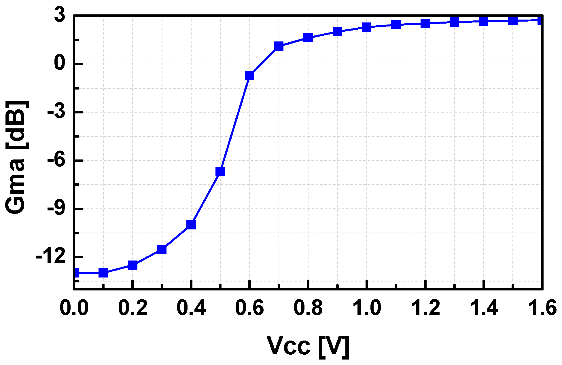
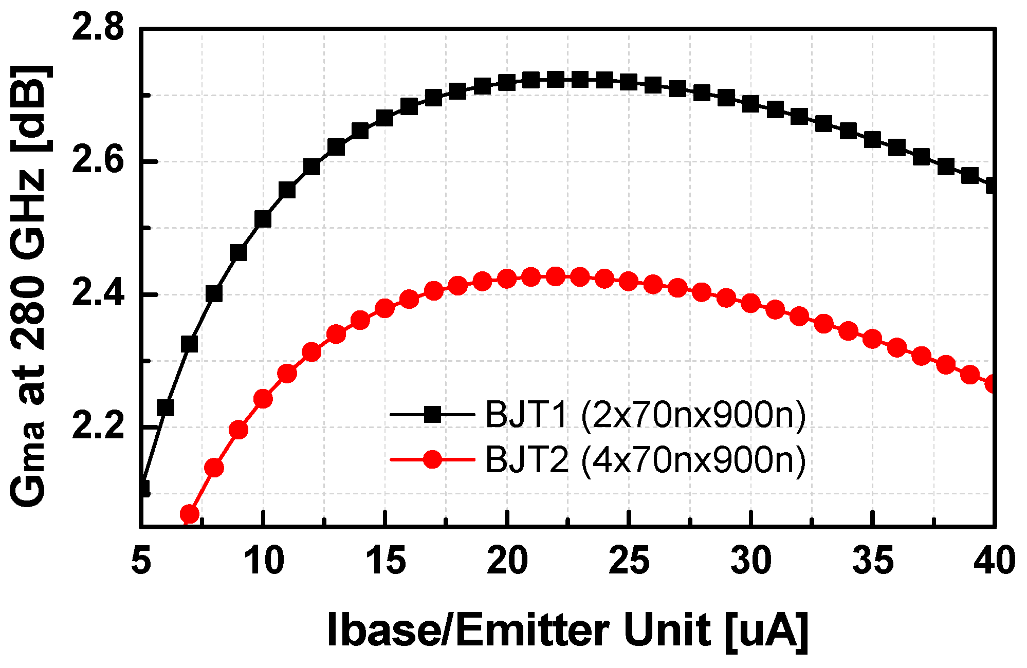
In the CE configuration, a higher supply voltage improves the gain, linearity, and output power of the amplifier with more power consumption. The supply voltage of 1.6-V was used for the CE amplifier, which is the maximum allowable DC voltage for the collector. Figure 3 presents the simulated Gma of the HBT with an emitter area of 2 × 70 nm × 900 nm versus Vcc at 280 GHz. The gain capability of the amplifier increases as Vcc rises. In this simulation setup, the base bias current was set to be 21 μA, corresponding to a base bias voltage of around 0.95 V. The base bias currents were provided via 1 kΩ resistors. Once Vcc was determined, the next step was to design a base bias for the CE amplifier. Figure 4 shows the simulated Gma at 280 GHz versus the normalized base bias current of two CE amplifiers using HBTs with an emitter size of 2 × 70 nm × 900 nm and 4 × 70 nm × 900 nm. It shows that both HBTs achieve the peak Gma at the base current of 20–25 μA over an emitter area unit of 2 × 70 nm × 900 nm. The larger HBT has a peak Gma of approximately 0.3 dB smaller than that of the smaller HBT. Based on this experiment, the HBT size of 2 × 70 nm × 900 nm with the base bias current of 21 μA was chosen for the amplifier.
2.2. Impedance Matching Network Design
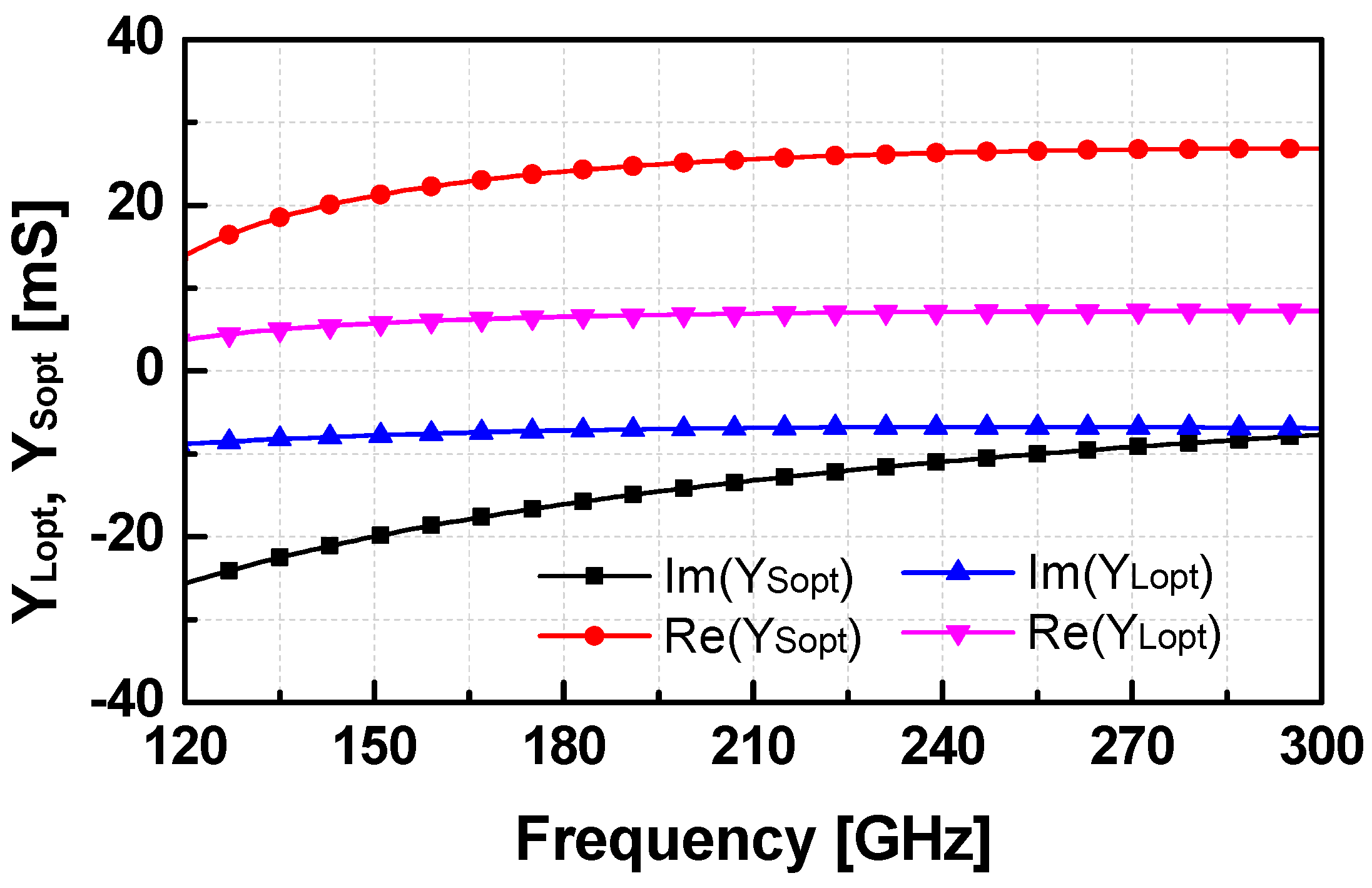
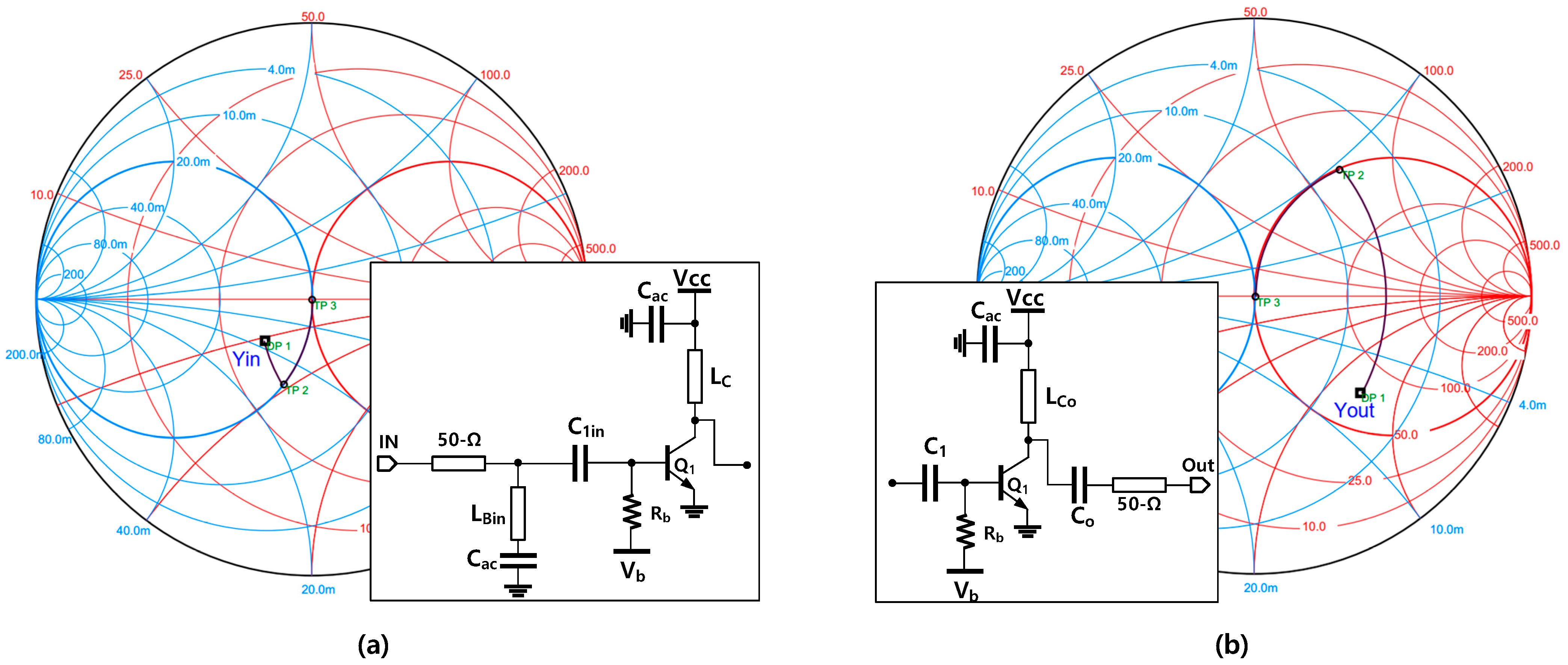
Figure 5 presents the optimum load and source admittances of the post-layout RC-extracted HBT with the emitter area of 2 × 70 nm × 900 nm. The optimum load and source admittances are given by
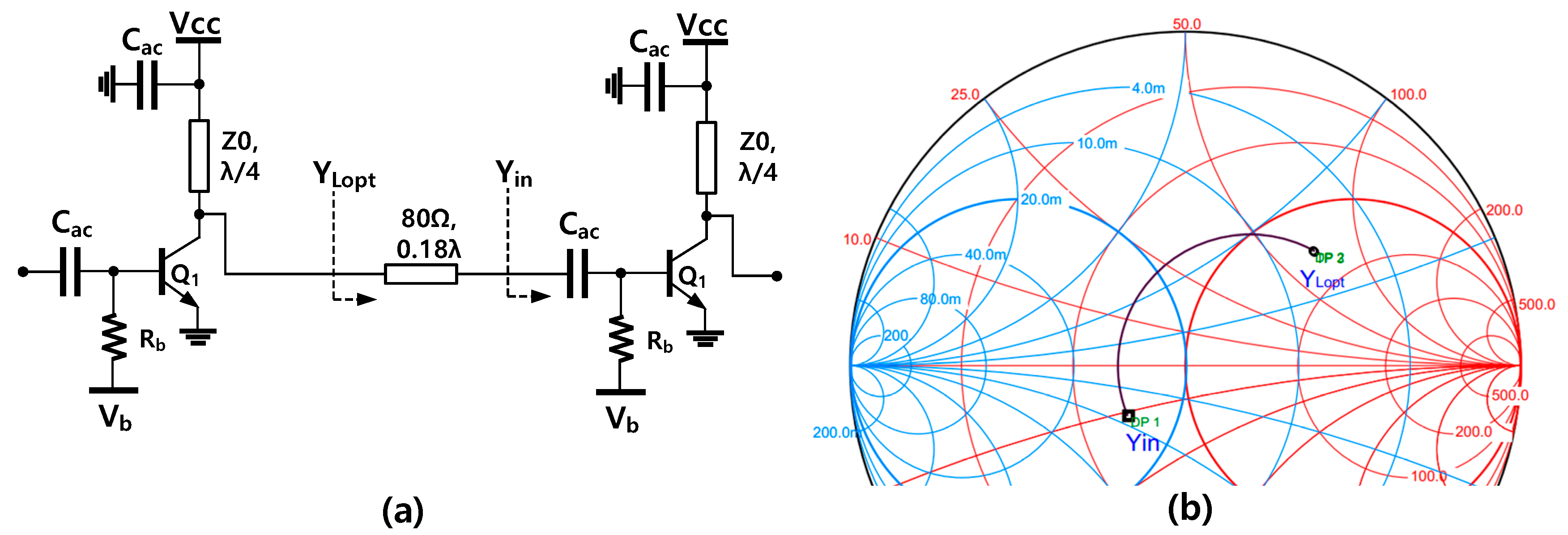
where Yin and Yout are the input and output admittances of the HBT. At 285 GHz, the extracted optimum source and load admittances are YSopt = 26.8−j8.41 (mS) and YLopt = 7.21 −j6.85 (mS), respectively. The input and output admittances of the HBT can be modeled as a resistor (Rp) in parallel with a capacitor (Cp). As observed, the input resistance (Rp_in) is smaller than the output resistance (Rp_out). The impedance matching task for the inter stages is to transform the input admittance (Yin = YSopt*) into the optimum load admittance (YLopt). The simplest impedance matching circuit is to use a series transmission line with proper characteristic impedance (Z0) to transform Yin into YLopt. The impedance transformation of this way is demonstrated on the Smith chart as shown in Figure 6a. This simple matching scheme has several disadvantages. First, if we use a transmission line connected between the collector and base of the next stage, it is required to use a big ac-coupling capacitor for DC-isolation between the two nodes. Second, a large collector bias current should be fed via the quarter wavelength transmission line to generate a high impedance for the collector node as shown in Figure 6b. The large size of the quarter wavelength transmission line is not preferred for a compact design considering the loss in the 300 GHz region. Moreover, the required length of the series transmission line is also relatively long for one stage (0.18λ turns to around 93 μm in physical length at 285 GHz).
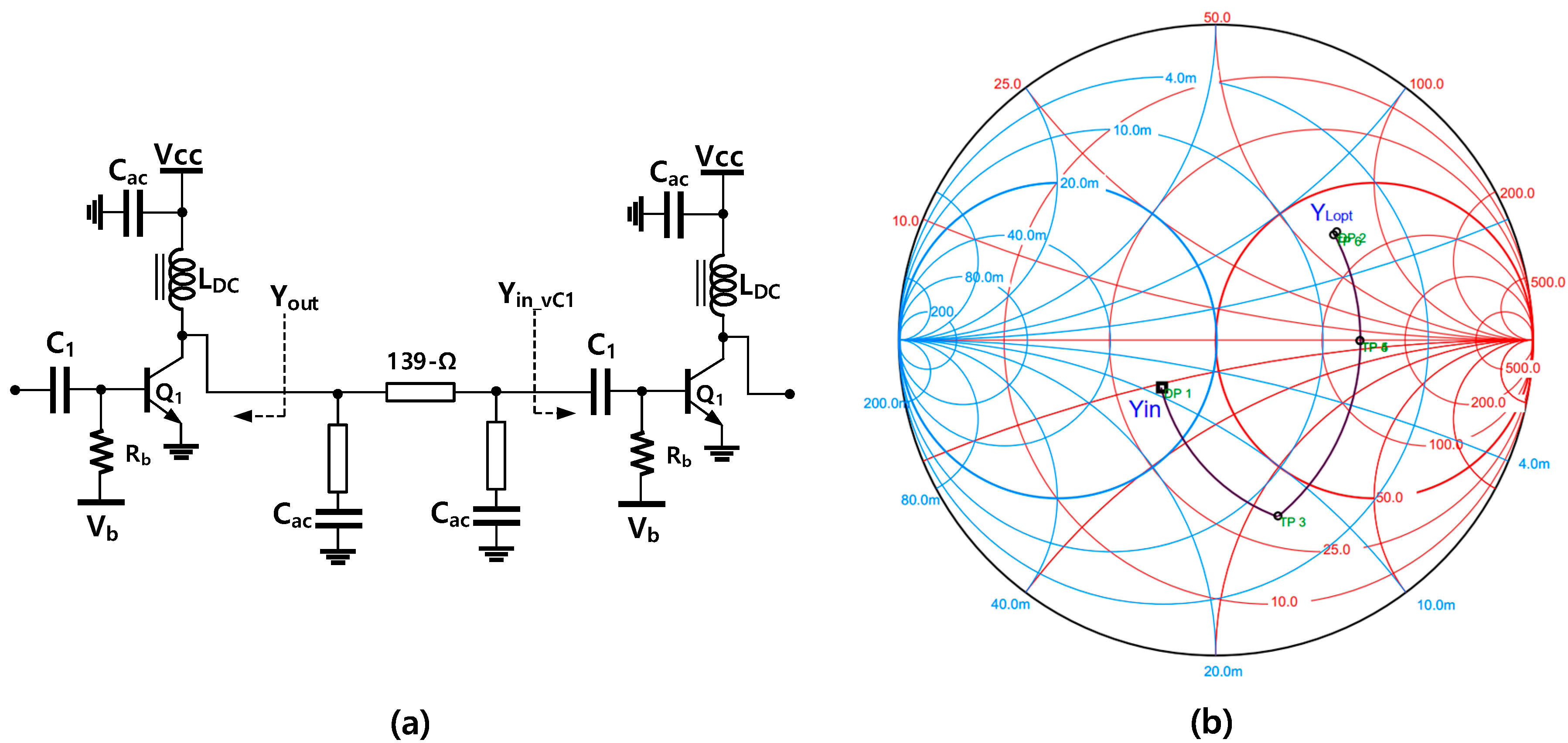
Figure 7 illustrates the flexible interstage impedance matching strategy used in this work and its impedance transformation on the smith chart. To eliminate the use of the large-size AC-coupling capacitor, a small series capacitor (named C1) can be involved in the interstage impedance matching. It is noted that the parallel input resistance at the base of the next stage is smaller than the required optimum output resistance at the collector, i.e., Rp_in < Rp_Lopt; the series matching capacitor in front of the base can transform the low parallel input resistance to a higher value. By selecting a proper value of C1, the transformed resistance can be exactly equal to Rp_Lopt. In detail, C1 was set by 11.4 fF, and the input admittance seen via C1 was Yin_vC1 = 7.21−j12.66 (mS) which is TP3 in Figure 7b. Then, a series stub as a resonating inductor can be used to resonate out the susceptance of Yin_vC1 and Yout. However, the length of the series stub is too short to properly place two HBTs considering the accuracy of the simulation at 300 GHz. To avoid this layout issue involved in a simple interstage matching, we employed two shunt short-stub as separate resonances for each imaginary part of Yin_vC1, and Yout, respectively, as presented in Figure 7a. Since C1 is chosen such that Rp_in_vC1 = 1/Re{Yin_vC1} = 1/Rp_Lopt, the two HBTs can be flexibly separated in an optimal distance using a T-line with the characteristic impedance of Z0 = 1/Rp_Lopt.
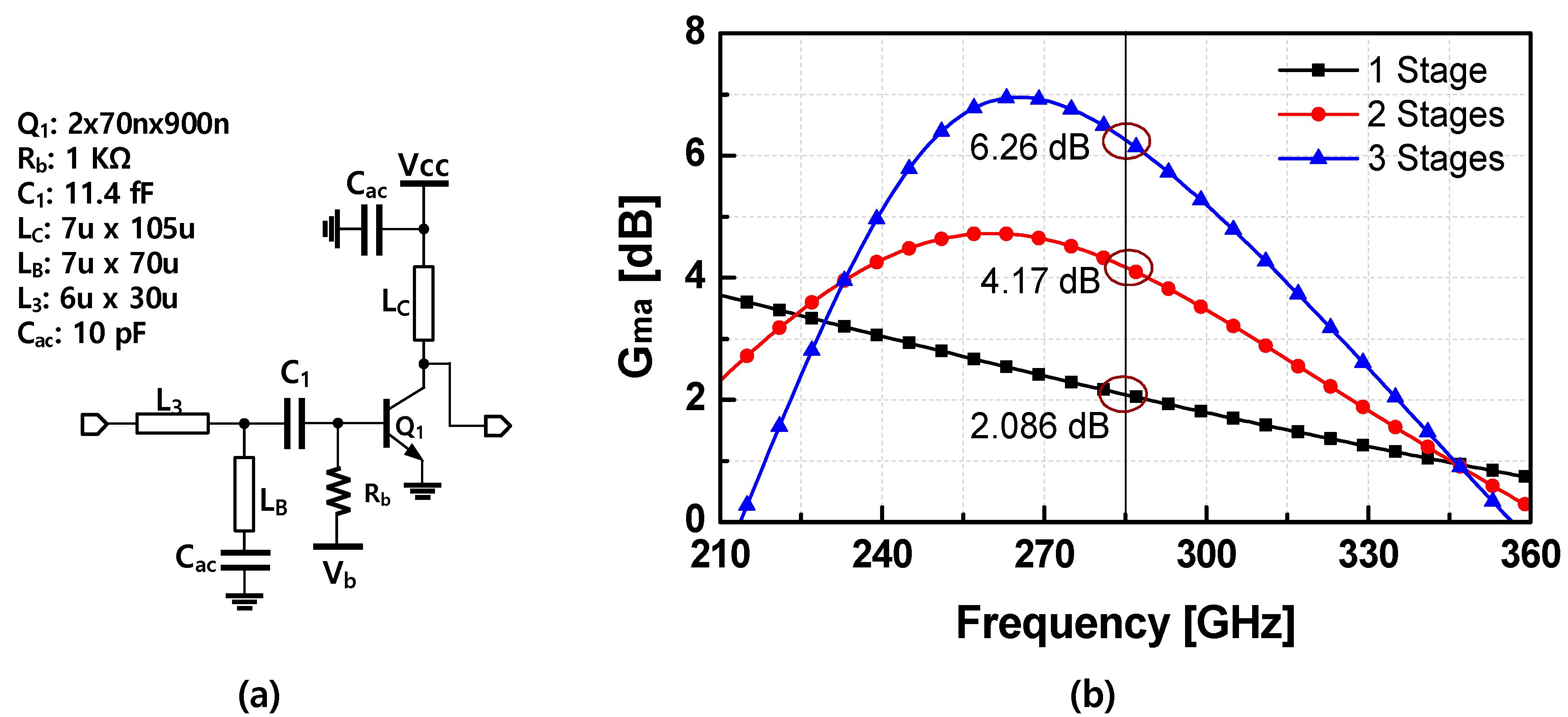
An impedance matching network with capacitors and T-lines provided by the PDK was used to verify the designed matching circuit as shown in Figure 8a. Since the T-line model considers the insertion loss, the circuit element values calculated previously were slightly different from the values from the ideal components. It is noteworthy that the T-line model from the PDK was found to be slightly optimistic compared to the EM simulation results. As can be seen, the Gma of the multiple stage amplifiers with two and three stages achieves twice and three times the Gma of the single stage at the target frequency of 285 GHz, which verifies the proposed interstage works well. Note that the plots of Gma versus frequency shows the peak Gma of around 267 GHz for the multi-stage amplifiers, and the peaking frequency of the 10-stage amplifier was simulated to be ~268 GHz. The peak at the lower center frequency is due to the −6 dB/oct roll-off characteristic of the Gma near the fmax. To compensate for the roll-off effect on the gain profile, the interstage impedance matching circuit should be implemented, aiming at a higher frequency to achieve a flat gain at the target frequency of 285 GHz.
For the input and output port, the impedance matching was carried out similarly to the interstage impedance matching, except that the aimed matching resistance was 50 Ω. The impedance transformation for the input impedance matching is demonstrated in Figure 9a. In the same procedure, the impedance matching network for the output was implemented with a shunt short stub with a T-line (LCo) to the collector and a series capacitor (Co), as shown in Figure 9b. For a short-stub implementation, relatively large bypass MIM capacitors were used.
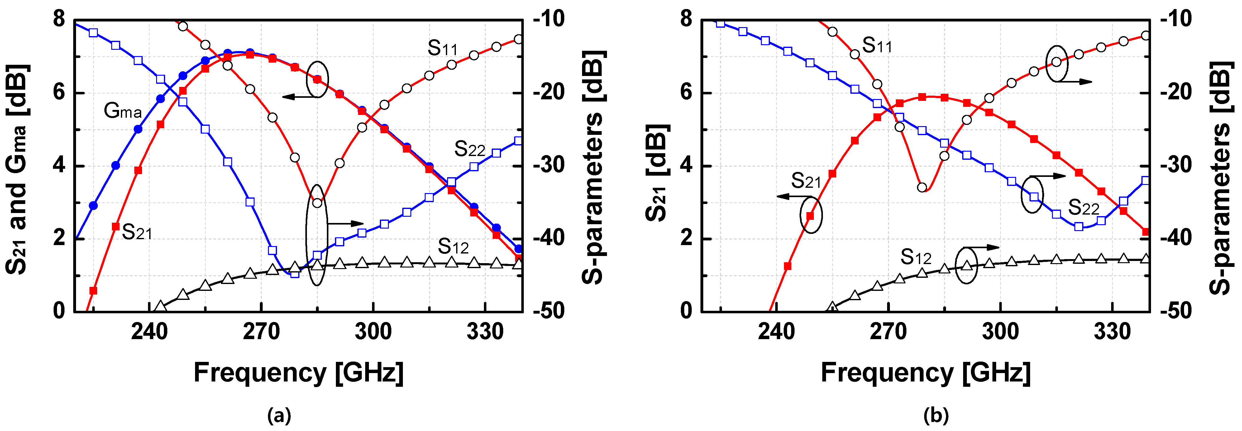
The simulated S-parameters of the three-stage amplifier with the designed input, interstage, and output impedance matching circuits on the schematic level are illustrated in Figure 10a. As observed, S11 and S22 were below −30 dB, and S21 was equal to Gma at 285 GHz. However, the simulation gain peaks at ~267 GHz which is similar to Gma. To flatten the gain at 285 GHz, the optimum impedance matching was performed at a higher frequency so that the peak gain could be tuned to 285 GHz. The simulated S-parameters of the three-stage cascaded amplifier are shown in Figure 10b. Around 0.47 dB of gain degradation was seen compared to the gain in the optimum impedance matching approach.
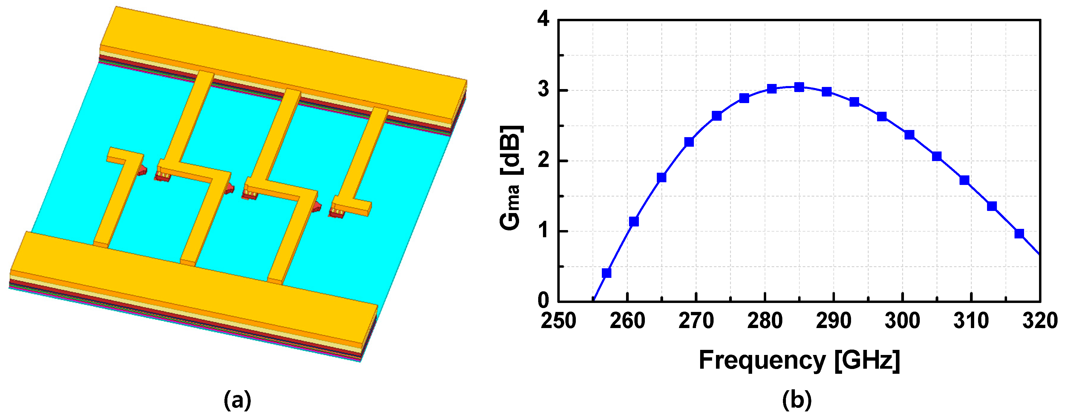
It is noted that the electrical contact between the base or collector of the HBT and the closest circuit elements always requires routing lines that exhibit parasitic inductances. Unfortunately, the RC-extractor used in the post-layout parasitics does not take parasitic inductances into account. In a sub-THz amplifier design, a pretty small amount of parasitic inductance effects significantly on the impedance, e.g., an inductance of 5 pH has an impedance of 9.42 Ω at 300 GHz. Meanwhile, the distance between the top metal layer to the bottom metal layer of the process is nearly 10 um, which gives a non-negligible effect via inductance for the layer-to-layer interconnections. These unwanted parasitic inductances would change the optimum load and source impedances compared to the previously reported values. In other words, the impedance matching circuits should also consider the electrical effect of these via connections. Moreover, the transmission lines simulated by HFSS have lower quality factors compared to the schematic model provided by the PDK. Considering these situations, the impedance matching networks of the amplifier were designed in co-simulation with the EM simulation results of the transmission lines on HFSS. The final design of the amplifier with the embedded matching circuits is presented in Figure 1. The impedance matching networks for the input and output were designed considering clear return current paths. A 3D EM model of the T-line-based matching networks of the three stages is shown in Figure 11a. Figure 11b depicts the Gma of three amplifying stages using the HFSS simulation results of T-lines. The peak value of Gma was ~3 dB seen at ~285-GHz. Hence, the loss from the passive components and via contacts is estimated to be around 3 dB compared with the results in Figure 10b.
3. Simulation and Measurement Results
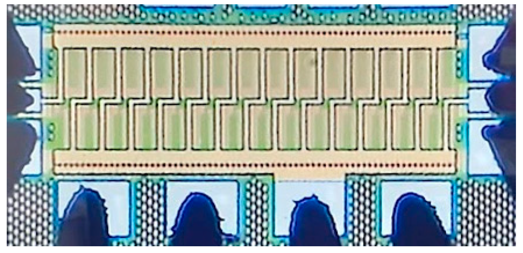
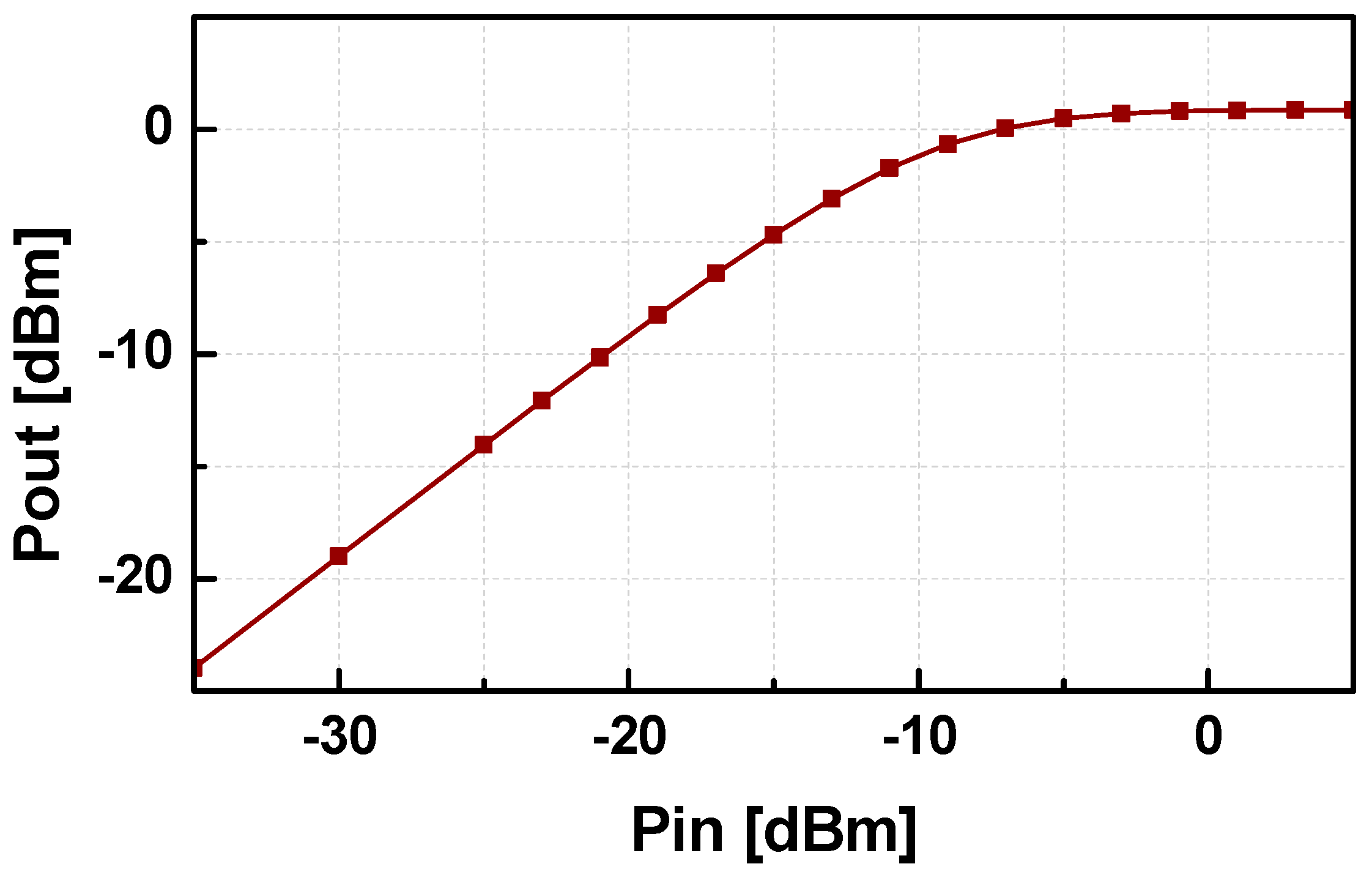
The proposed 280 GHz amplifier was designed in 130 nm SiGe technology with an fT/fmax of 350/450 GHz. Figure 12 shows a photo of the fabricated amplifier, which occupies an area of 0.71 × 0.3 mm2, including all the pads. The amplifier consumes a DC current of 62 mA from a 1.6 V supplier. A continuous wave (CW) measurement was used to measure the gain of the amplifier. The input signal was generated from a frequency multiplier SGX VDI 2.8 combined with a signal generator Agilent 83623B. An integrated thru was used to calibrate the loss of GGB probes and waveguides. The output power of the amplifier was characterized by an Erickson calorimeter (VDI PM-5). Figure 13 shows the simulation results of the noise figure and s-parameters of the amplifier in comparison with the measured gain. As can be seen, the measured gain fits well with the simulation results. The maximum measured gain was 10.9 dB recorded at 283 GHz. The 3 dB gain’s bandwidth was 30 GHz from 270 to 300 GHz. In the simulation, S11 and S22 are smaller than −10 dB in the operation range. Meanwhile, the simulated NF was minimized by 15.9 dB at ~286 GHz. The simulated output power of the amplifier at 283 GHz versus the input power is shown in Figure 14. The amplifier achieved an input 1 dB gain compression point (IP1dB) of −13.5 dBm, which corresponded to an output of 1 dB gain compression point (OP1dB) of around −3.6 dBm.
The performance of the implemented amplifier is summarized compared with recent amplifiers in similar frequency bands in Table 1. As shown in the table, the applied SiGe technologies for the recently reported sub-THz amplifiers were more advanced than our work except [24]. Compared with our work, the design in [24] achieved a 2 dB higher gain at the cost of the higher DC power consumption. Other performances are comparable with our work. For the work in [23], the SiGe technology with a much higher fmax can explain the better performance it attained. The architecture in [23] is similar to the work in [26], and its gain-bandwidth improvement was due to the much larger DC-power consumption compared with our design.
4. Conclusions
We presented a 280-GHz driving amplifier in 130-nm SiGe technology. The common emitter (CE) configuration with embedded interstage matching networks was co-designed to achieve a compact area and improved noise performance at the cost of a relatively low gain-per-stage performance. To compensate for this shortage, the amplifier comprises 14 stages of common-emitter amplifiers with flexible interstage-matching networks. Owing to the presented interstage matching strategy, the whole amplifier occupies only 0.213 mm2, including all the RF and DC pads. Owing to the elaborated layout, considering a clear return current path and via parasitics in HFSS simulation, the measured amplifier demonstrated a power gain of 10.9 dB with a 3 dB gain bandwidth of 30 GHz between 270 and 300 GHz which corresponds well with the simulations. In the simulation, the amplifier attained a peak output power of 0.8 dBm and an output of 1 dB compression point of -3.6 dBm. The proposed amplifier and its design strategy can be effectively applied to the integrated sub-THz transceiver designs.
Author Contributions
Data curation, V.-S.T. and J.-M.S.; conceptualization and supervision, J.-D.P.; validation, V.-S.T. and J.-M.S.; writing—original draft, V.-S.T.; writing—review and editing, J.-D.P. All authors have read and agreed to the published version of the manuscript.
Funding
This work was supported by Electronics and Telecommunications Research Institute (ETRI) grant funded by the Korean government [22ZH1100, Study on 3D communication technology for hyper-connectivity].
Acknowledgments
The authors thank Sooyeon Kim, Seung Hwan Kim, and Seung-Hyun Cho in Optical Network Research Section, Electronics and Telecommunications Research Institute (ETRI) for the measurement support.
Conflicts of Interest
The authors declare no conflict of interest. The funders had no role in the design of the study; in the collection, analyses, or interpretation of data; in the writing of the manuscript, or in the decision to publish the results.
References
- Kissinger, D.; Kahmen, G.; Weigel, R. Millimeter-wave and terahertz transceivers in SiGe BiCMOS technologies. IEEE Trans. Microw. Theory Technol. 2021, 69, 4541–4560. [Google Scholar] [CrossRef]
- Wallace, V.P.; Fitzgerald, A.J.; Shankar, S.; Flanagan, N.; Pye, R.; Cluff, J.; Arnone, D.D. Terahertz pulsed imaging of basal cell carcinoma ex vivo and in vivo. Br. J. Dermatol. 2004, 151, 424–432. [Google Scholar] [CrossRef]
- Pickwell, E.; Wallace, V.P. Biomedical applications of terahertz technology. J. Phys. D Appl. Phys. 2006, 39, R301–R310. [Google Scholar] [CrossRef]
- Ashish, Y.P.; Deepak, D.S.; Kiran, B.E.; Deelip, V.D. Terahertz technology and its applications. Drug Invent. Today 2013, 5, 157–163. [Google Scholar]
- Petrov, V.; Kurner, T.; Hosako, I. IEEE 802.15.3d: First Standardization Efforts for Sub-Terahertz Band Communications toward 6G. IEEE Commun. Mag. 2020, 58, 28–33. [Google Scholar] [CrossRef]
- Rappaport, T.S.; Xing, Y.; Kanhere, O.; Ju, S.; Madanayake, A.; Mandal, S.; Alkhateeb, A.; Trichopoulos, G.C. Wireless communications and applications above 100 GHz: Opportunities and challenges for 6G and beyond. IEEE Access 2019, 7, 78729–78757. [Google Scholar] [CrossRef]
- Moon, S.-R.; Kim, E.-S.; Sung, M.; Rha, H.Y.; Lee, E.S.; Lee, I.-M.; Park, K.H.; Lee, J.K.; Cho, S.-H. 6G Indoor Network Enabled by Photonics- and Electronics-Based sub-THz Technology. J. Lightwave Technol. 2022, 40, 499–510. [Google Scholar] [CrossRef]
- Abdo, I.; Fujimura, T.; Miura, T.; Tokgoz, K.K.; Hamada, H.; Nosaka, H.; Shirane, A.; Okada, K. A 300 GHz wireless transceiver in 65 nm CMOS for IEEE 802.15.3d using push-push subharmonic mixer. In Proceedings of the IEEE/MTT-S International Microwave Symposium (IMS), Los Angeles, CA, USA, 4–6 August 2020; pp. 623–626. [Google Scholar]
- Eissa, M.H.; Maletic, N.; Grass, E.; Kraemer, R.; Kissinger, D.; Malignaggi, A. 100 Gbps 0.8-m Wireless Link based on Fully Integrated 240 GHz IQ Transmitter and Receiver. In Proceedings of the IEEE/MTT-S International Microwave Symposium (IMS), Los Angeles, CA, USA, 4–6 August 2020; pp. 627–630. [Google Scholar]
- Rodríguez, P.; Vázquez; Grzyb, J.; Heinemann, B.; Pfeiffer, U.R. A 16-QAM 100-Gb/s 1-M Wireless Link With an EVM of 17% at 230 GHz in an SiGe Technology. IEEE Microw. Wirel. Compon. Lett. 2019, 29, 297–299. [Google Scholar] [CrossRef]
- Janusz, G.; Pedro, R.-V.; Stefan, M.; Marcel, A.; Ullrich, R.P. A SiGe HBT 215–240 GHz DCA IQ TX/RX Chipset With Built-In Test of USB/LSB RF Asymmetry for 100+ Gb/s Data Rates. IEEE Trans. Microw. Theory Tech. 2022, 70, 1696–1714. [Google Scholar]
- Rodriguez-Vazquez, P.; Grzyb, J.; Heinemann, B.; Pfeiffer, U.R. A QPSK 110-Gb/s Polarization-Diversity MIMO Wireless Link With a 220–255 GHz Tunable LO in a SiGe HBT Technology. IEEE Trans. Microw. Theory Tech. 2020, 68, 3834–3851. [Google Scholar] [CrossRef]
- Eissa, M.H.; Malignaggi, A.; Wang, R.; Elkhouly, M.; Schmalz, K.; Ulusoy, A.C.; Kissinger, D. Wideband 240-GHz transmitter and receiver in BiCMOS technology with 25-Gbit/s data rate. IEEE J. Solid-State Circuits 2018, 53, 2532–2542. [Google Scholar] [CrossRef]
- Wang, Y.; Yu, B.; Ye, Y.; Chen, C.-N.; Gu, Q.J.; Wang, H. A G-Band on-off-Keying Low-Power Transmitter and Receiver for Interconnect Systems in 65-nm CMOS. IEEE Trans. Terahertz Sci. Technol. 2020, 10, 118–132. [Google Scholar] [CrossRef]
- Schmalz, K.; Rothbart, N.; Gluck, A.; Eissa, M.H.; Mausolf, T.; Turkmen, E.; Yilmaz, S.B.; Hubers, H.-W. Dual-Band Transmitter and Receiver with Bowtie-Antenna in 0.13 μm SiGe BiCMOS for Gas Spectroscopy at 222–270 GHz. IEEE Access 2021, 9, 124805–124816. [Google Scholar] [CrossRef]
- Yu, J.; Chen, J.; Zhou, P.; Li, Z.; Li, H.; Yan, P.; Hou, D.; Hong, W. A 300-GHz Transmitter Front End With −4.1-dBm Peak Output Power for Sub-THz Communication Using 130-nm SiGe BiCMOS Technology. IEEE Trans. Microw. Theory Tech. 2021, 69, 4925–4936. [Google Scholar] [CrossRef]
- Hadidian, B.; Khoeini, F.; Hossein, S.M.; Andreia, C.; Afshari, E. A 220-GHz Energy-Efficient High-Data-Rate Wireless ASK Transmitter Array. IEEE J. Solid-State Circuits 2022, 57, 1623–1634. [Google Scholar] [CrossRef]
- Alakusu, U.; Dadash, M.S.; Shopov, S.; Chevalier, P.; Cathelin, A.; Voinigescu, S.P. A 210–284-GHz I–Q Receiver With On-Chip VCO and Divider Chain. IEEE Microw. Wirel. Compon. Lett. 2020, 30, 50–53. [Google Scholar] [CrossRef]
- Vazquez, P.R.; Grzyb, J.; Sarmah, N.; Heinemann, B.; Pfeiffer, U.R. A 219–266 GHz fully-integrated direct-conversion IQ receiver module in a SiGe HBT technology. In Proceedings of the 12th European Microwave Integrated Circuits Conference (EuMIC), Nuremberg, Germany, 8–10 October 2017; pp. 261–264. [Google Scholar]
- Elkhouly, M.; Mao, Y.; Glisic, S.; Meliani, C.; Ellinger, F.; Scheytt, J.C. A 240 GHz direct conversion IQ receiver in 0.13 μm SiGe BiCMOS technology. In Proceedings of the IEEE Radio Frequency Integrated Circuits Symposium (RFIC), Seattle, WA, USA, 2–4 June 2013; pp. 305–308. [Google Scholar]
- Thyagarajan, S.V.; Kang, S.; Niknejad, A.M. A 240 GHz fully integrated wideband QPSK receiver in 65 nm CMOS. IEEE J. Solid-State Circuits 2015, 50, 2268–2280. [Google Scholar] [CrossRef]
- Tokgoz, K.K.; Abdo, I.; Fujimura, T.; Pang, J.; Kawano, Y.; Iwai, T.; Kasamatsu, A.; Watanabe, I.; Okada, K. A 273–301-GHz amplifier with 21-dB peak gain in 65-nm standard bulk CMOS. IEEE Microw. Wirel. Compon. Lett. 2019, 29, 342–344. [Google Scholar] [CrossRef]
- Park, D.; Utomo, D.R.; Lam, B.H.; Hong, J.; Lee, S. A 280-/300-GHz three-stage amplifiers in 65-nm CMOS with 12-/9-dB gain and 1.6/1.4% PAE while dissipating 17.9 mW. IEEE Microw. Wirel. Compon. Lett. 2018, 28, 79–81. [Google Scholar] [CrossRef]
- Gadallah, A.; Eissa, M.H.; Mausolf, T.; Kissinger, D.; Malignaggi, A. A 300-GHz Low-Noise Amplifier in 130-nm SiGe SG13G3 Technology. IEEE Microw. Wirel. Compon. Lett. 2022, 32, 331–334. [Google Scholar] [CrossRef]
- Singh, S.P.; Rahkonen, T.; Leinonen, M.E.; Pärssinen, A. A 290 GHz low noise amplifier operating above fmax /2 in 130 nm SiGe technology for sub-THz/THz receivers. In Proceedings of the IEEE Radio Frequency Integrated Circuits Symposium (RFIC), Atlanta, GA, USA, 7–9 June 2021; pp. 223–226. [Google Scholar]
- Malz, S.; Hillger, P.; Heinemann, B.; Pfeiffer, U.R. A 275 GHz amplifier in 0A3 μm SiGe. In Proceedings of the 11th European Microwave Integrated Circuits Conference (EuMIC), London, UK, 3–4 October 2016; pp. 185–188. [Google Scholar]
- Li, X.; Chen, W.; Zhou, P.; Wang, Y.; Huang, F.; Li, S.; Chen, J.; Feng, Z. A 250–310 GHz Power Amplifier With 15-dB Peak Gain in 130-nm SiGe BiCMOS Process for Terahertz Wireless System. IEEE Trans. Terahertz Sci. Technol. 2022, 12, 1–12. [Google Scholar] [CrossRef]
- Heydari, B. CMOS Circuits and Devices beyond 100 GHz. Ph.D. Thesis, UC Berkeley, Berkeley, CA, USA, 2008. [Google Scholar]
Figure 1.
Schematic of the 280 GHz amplifier.

Figure 2.
Power gains and stability factor of a post-layout extracted HBT with the emitter size of 2 × 70 nm × 900 nm.
Figure 2.
Power gains and stability factor of a post-layout extracted HBT with the emitter size of 2 × 70 nm × 900 nm.

Figure 3.
Simulated Gma at 280 GHz of the transistor (2 × 70 nm × 900 nm) versus supply voltage when the base bias current is fixed to 21 μA.
Figure 3.
Simulated Gma at 280 GHz of the transistor (2 × 70 nm × 900 nm) versus supply voltage when the base bias current is fixed to 21 μA.

Figure 4.
Simulated maximum available gain (Gma) at 280 GHz of HBTs versus the base bias current which is scaled with the emitter size of 2 × 70 nm × 900 nm as a unit).
Figure 4.
Simulated maximum available gain (Gma) at 280 GHz of HBTs versus the base bias current which is scaled with the emitter size of 2 × 70 nm × 900 nm as a unit).

Figure 5.
Optimum load and source admittances of post-layout RC-extracted HBT (2 × 70 nm × 900 nm) for the gain matching.
Figure 5.
Optimum load and source admittances of post-layout RC-extracted HBT (2 × 70 nm × 900 nm) for the gain matching.

Figure 6.
A simple interstage impedance matching circuit: (a) the possible circuit implementation, (b) impedance transformation on smith chart.
Figure 6.
A simple interstage impedance matching circuit: (a) the possible circuit implementation, (b) impedance transformation on smith chart.

Figure 7.
Circuit structure for interstage impedance matching (a) and impedance transformation using on smith chart (b).
Figure 7.
Circuit structure for interstage impedance matching (a) and impedance transformation using on smith chart (b).

Figure 8.
One amplifier unit with interstage impedance matching circuit on schematic level (a) and the simulated maximum available gain (Gma) of 1, 2, and 3 stages (b).
Figure 8.
One amplifier unit with interstage impedance matching circuit on schematic level (a) and the simulated maximum available gain (Gma) of 1, 2, and 3 stages (b).

Figure 9.
Impedance matching for the input (a) and the output (b) on the schematic level.

Figure 10.
Simulated S-parameters and Gma of the three-stage amplifier (using passive devices at the schematic level) with conventional interstage matching at 285 GHz (a) and flexible interstage matching for a flat gain at 285 GHz (b).
Figure 10.
Simulated S-parameters and Gma of the three-stage amplifier (using passive devices at the schematic level) with conventional interstage matching at 285 GHz (a) and flexible interstage matching for a flat gain at 285 GHz (b).

Figure 11.
3D HFSS model for EM simulation of three impedance matching stages (a), and Gma of three amplifying stages using EM simulated T-lines (b).
Figure 11.
3D HFSS model for EM simulation of three impedance matching stages (a), and Gma of three amplifying stages using EM simulated T-lines (b).

Figure 12.
A photograph of the 280 GHz amplifier.

Figure 13.
Simulation results of S-parameters and noise figure (NF) and measured gain of the amplifier.
Figure 13.
Simulation results of S-parameters and noise figure (NF) and measured gain of the amplifier.

Figure 14.
Simulated output power versus input power of the amplifier at 283 GHz.


Table 1.
Summary of State-Of-Art Amplifiers Around 280 GHz.
| Ref. | Tech. | ft/fmax | Freq. (GHz) | Topology | BW (GHz) | Gain (dB) | Minimum NF * (dB) | IP1dB (dBm) | Area (mm2) | PDC [mW] |
|---|---|---|---|---|---|---|---|---|---|---|
| This | 130 nm SiGe | 350/450 | 270–300 | CE, SE | 30 | 10.9 | 15.9 | −13.5 * | 0.21 | 99.2 |
| [22] | 65 nm CMOS | 250/300 | 297.5 | CS, SE | 1 | 21 | 10 | −34 | 1.12 | 35.4 |
| [23] | 65 nm CMOS | NA/395 * | 280 | CS, SE | ~10 ** | 12 | NA | −16.9 | 0.14 | 17.9 |
| [24] | 130 nm SiGe | 470/700 | 291 | CC, Diff. | 68 | 10.8 | 11 | −15.6 | 0.26 | 119 |
| [25] | 130 nm SiGe | 300/450 | 290 | CC, Diff. | 23 | 12.9 | 16 | −9 | 0.25 | 136 |
| [26] | 130 nm SiGe | 350/550 | 275 | CE, Diff. | 7 | 10 | 18 | −10 | 0.35 | 122.7 |
| [27] | 130 nm SiGe | 300/500 | 290 | CC, Diff. | 67 | 15 | NA | −12 | 0.57 | 267.5 |
* Simulated; ** estimated from figure; CE: common emitter; SE: single-ended; CC: cascode; CS: common source.
Publisher’s Note: MDPI stays neutral with regard to jurisdictional claims in published maps and institutional affiliations. |
© 2022 by the authors. Licensee MDPI, Basel, Switzerland. This article is an open access article distributed under the terms and conditions of the Creative Commons Attribution (CC BY) license (https://creativecommons.org/licenses/by/4.0/).
Share and Cite
MDPI and ACS Style
Trinh, V.-S.; Song, J.-M.; Park, J.-D. A 280 GHz 30 GHz Bandwidth Cascaded Amplifier Using Flexible Interstage Matching Strategy in 130 nm SiGe Technology. Electronics 2022, 11, 3045. https://doi.org/10.3390/electronics11193045
AMA Style
Trinh V-S, Song J-M, Park J-D. A 280 GHz 30 GHz Bandwidth Cascaded Amplifier Using Flexible Interstage Matching Strategy in 130 nm SiGe Technology. Electronics. 2022; 11(19):3045. https://doi.org/10.3390/electronics11193045
Chicago/Turabian StyleTrinh, Van-Son, Jeong-Moon Song, and Jung-Dong Park. 2022. "A 280 GHz 30 GHz Bandwidth Cascaded Amplifier Using Flexible Interstage Matching Strategy in 130 nm SiGe Technology" Electronics 11, no. 19: 3045. https://doi.org/10.3390/electronics11193045
Note that from the first issue of 2016, this journal uses article numbers instead of page numbers. See further details here.