Article

Using Overlapped Resonators in Wireless Power Transfer for Uniform Electromagnetic Field and Removing Blank Spots in Free Moving Applications

by
Saeideh Pahlavan
1,
Mostafa Shooshtari
2,*,
Mohammadreza Maleki
3 and
Shahin Jafarabadi Ashtiani
1
1
School of Electrical and Computer Engineering, College of Engineering, University of Tehran, Tehran 14395-515, Iran
2
Laboratory of Electronic Components, Department of Microelectronics, Technology and Materials (ECTM), Delft University of Technology, 2628 CD Delft, The Netherlands
3
Department of Electrical, Computer, and Biomedical Engineering, Faculty of Engineering, Ryerson University, Toronto, ON M5B 2K3, Canada
*
Author to whom correspondence should be addressed.
Electronics 2022, 11(8), 1204; https://doi.org/10.3390/electronics11081204
Submission received: 25 February 2022 / Revised: 29 March 2022 / Accepted: 8 April 2022 / Published: 10 April 2022

Abstract

:
We propose an induction link based on overlapping arrays to eliminate blank spots on the electromagnetic field for moving object applications. We use two arrays of four aligned coils that have a 50% overlap between the two plates. This mechanism compensates for the internal coil power drop at positions in the boundaries between two adjacent external coils. We showed that if these plates are excited, a uniform electromagnetic field is created in the movement direction of the moving object. This uniform electromagnetic field distribution will result in a constant receiving power at all points in the path of the moving internal coil with the same power consumption of one coil excitation. Power delivery to the moving object tolerance reaches 10% at most, while, in non-overlapped scenarios, it is approximately 50%. In addition, according to the theoretical calculations, printed circuit coils (PCB) for the array are designed for maximum efficiency. We found that the change in distance and dimensions of the receiver coil has a linear effect on power and efficiency. Moreover, a Specific Absorption Rate (SAR) simulation was performed for biocompatibility. In this paper, we investigate and record a 68% electrical power efficiency for the fabricated system. The array consists of eight transmitters coils of the same size and shape and a receiver coil at a distance of 4 cm. Furthermore, the fabricated coil has shown improved efficiency compared to similar studies in the literature and introduces a promising structure for bio-test applications.

1. Introduction

The technology that enables transmitting energy to an electric load wirelessly is known as Wireless Power Transfer (WPT) [1]. WPT has found many applications in various scientific fields such as bioelectronics [2,3,4] and the study of living animal behavior [5]. Inductive WPT is an alternative to replace the tethering cable with power implants in the human body [6]. WPT can also be a suitable alternative to existing traditional charging systems. For example, in bio-implants, rechargeable batteries with a smaller capacity, size, and more stability can be used instead of non-rechargeable batteries to reduce the number of surgeries for battery replacement [7].
The inductive WPT system consists of three main parts. The first part consists of a pulse generator and a Power Amplifier (PA) that converts DC to AC power and delivers it to the power transmission coil on the primary side. The second part is called the induction link, which is composed of two coils for power transmission, as well as magnetic coupling between them. Typically, there are two coils in the second part of the inductive WPT technique: Implanted and external coils. The implanted coil often has a small size and is placed in the body to receive power from an external coil. Finally, the third part is an AC-to-DC converter (rectifier) that delivers the AC power received from the induction link as DC power to the system load [8,9].
Power transmission uniformity is necessary to avoid interruption of the moving load during its operation [10]. Thus, the moving internal coil (as load) requires a free positioning area wherein it can move freely and receive the required power. In free-moving applications, there are two methods to deliver power to a moving target: First, using a single transmitter coil that is big enough to cover the moving internal coil route [5]; second, using a transmitter array [11]. Using a big coil is not a solution to creating uniform fields in the moving internal coil (receiver). The resultant field distribution is strong at the coil center and drops at the borders [12]. Therefore, the technique is not reasonably efficient. The second idea, i.e., using array coils, has the advantage of higher Power Transfer Efficiency (PTE); it can also track the receiver coil position so as to deliver power, particularly to the coil at the position with optimal PTE [13]. However, the presence of black spots causes a non-uniform electromagnetic field in the coil array. The interaction of the vector fields in the neighboring borders of the two adjacent transmitter coils causes the minimization of the resultant fields at these points. Therefore, the power delivered to the moving object decreases dramatically at these points. These points are defined as power blank spots. Extending the charge time or disconnecting the charging is the result of power transmission non-uniformity and blank spots [14].
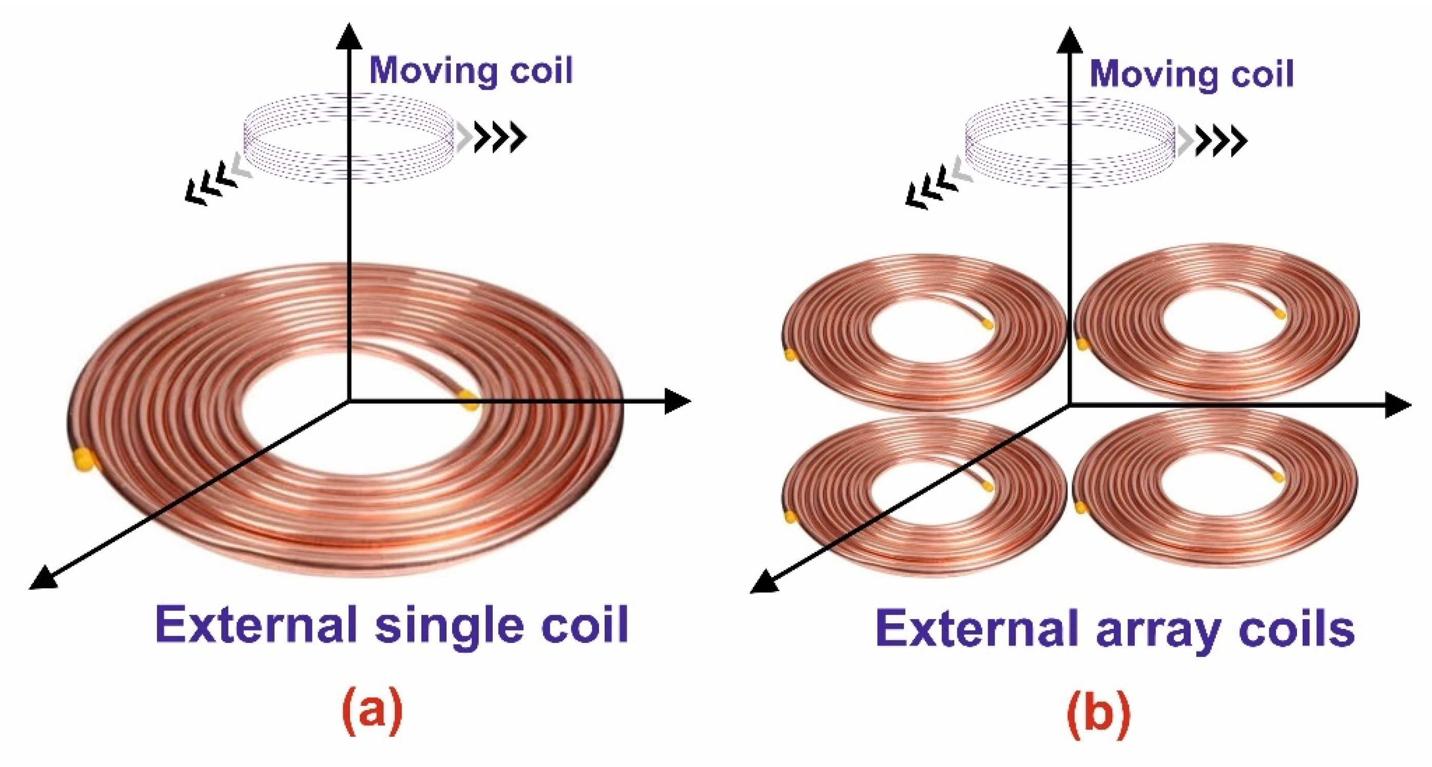
Figure 1 shows the schematic of the moving load, which is extensively used in biomedical applications ranging from capsule endoscopy [15] to optogenetics [16]. A big single coil with a moving coil shown in 
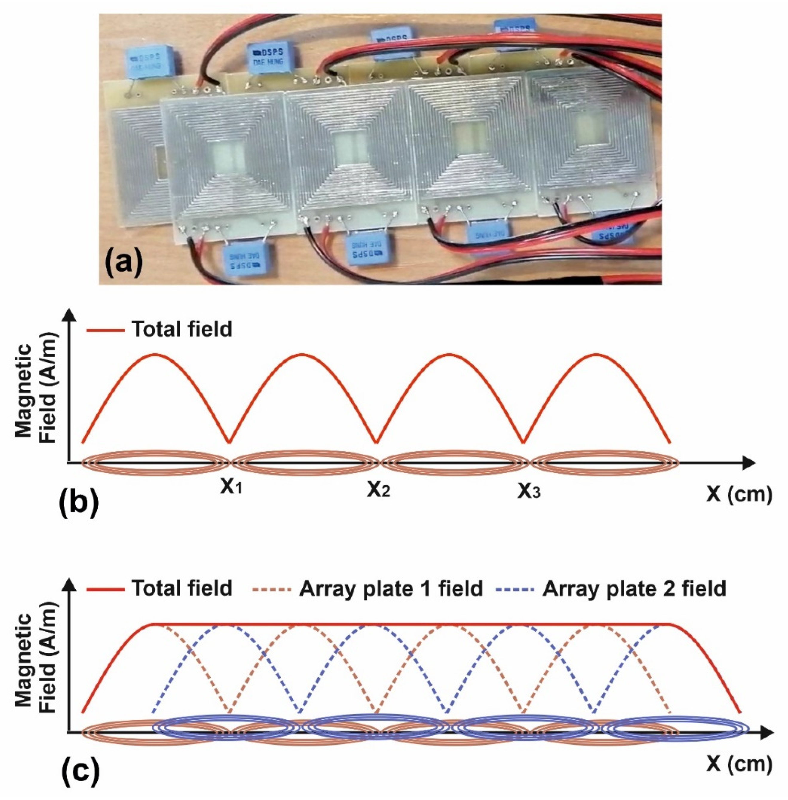
Figure 1a causes misalignment between the external and moving internal coils. Moreover, the Gaussian distribution of this field creates blank spots at bigger coil borders. It can significantly impact both the charging efficiency and time. Therefore, by using smaller-sized external array coils, the Gaussian field distribution is broken into several Gaussian fields and creates a more uniform field distribution. The multi-coils shown in Figure 1b are in the form of an array to create a uniform field for the application of free-moving objects, as discussed earlier.
Extensive research has been performed to study inductive WPT devices with three, four [17], and even more external coils [18]. Different topologies in array structures have been able to cover a large area, and various methods have been proposed for power transmission uniformity and the elimination of blank spots [19,20]. The most important ideas in the literature concern proposing models for the electrical excitement of external coils via a power supply [21]. Although these methods are effective in eliminating blank spots, the uniformity of the power transmission still remains a major challenge. In addition, by tracking the internal coil, only the neighboring external arrays can be turned on, and this increases the PTE and reduces power consumption. The tracking mechanism of internal coils has received less attention from researchers.
In this paper, we design and characterize a transmitter array composed of eight coils that are excited separately as an inductive WPT source for a moving coil. These eight coils are placed on top of each other in two layers with 50% overlap. We show the superior performance of the structure over other solutions to achieve uniformity of power transmission. Eliminating black spots and creating a uniform field for the application of a free-moving object while maintaining high efficiency is the main achievement of this research.
Optimal coils and links are designed using theoretical equations in Section 2 based on the circuit model of the inductive link. Then the array structure for these designed coils in free-moving objects is used. The field distributions of overlapped and non-overlapped array structures are compared over the movement direction of the internal coil in Section 3. Furthermore, a tracking mechanism based on feedback is applied for moving objects to increase the efficiency of the system. The simulations and measurement results of fabricated circuits and systems are compared and demonstrated in Section 4 via theoretical analysis. The conclusions drawn about the overlapping array are presented in Section 5.

2. Theoretical Model of Inductive Power Transmission

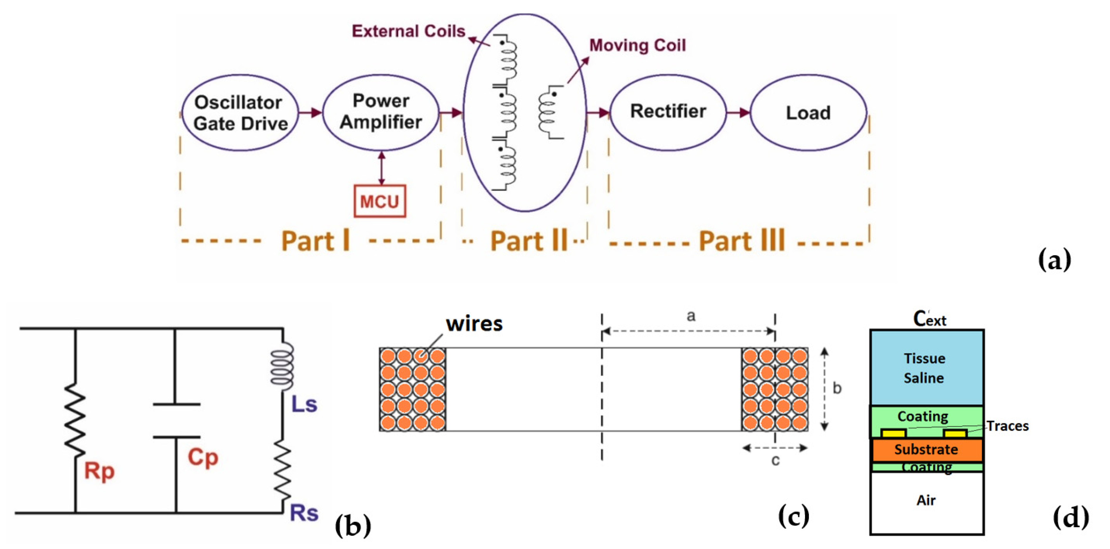
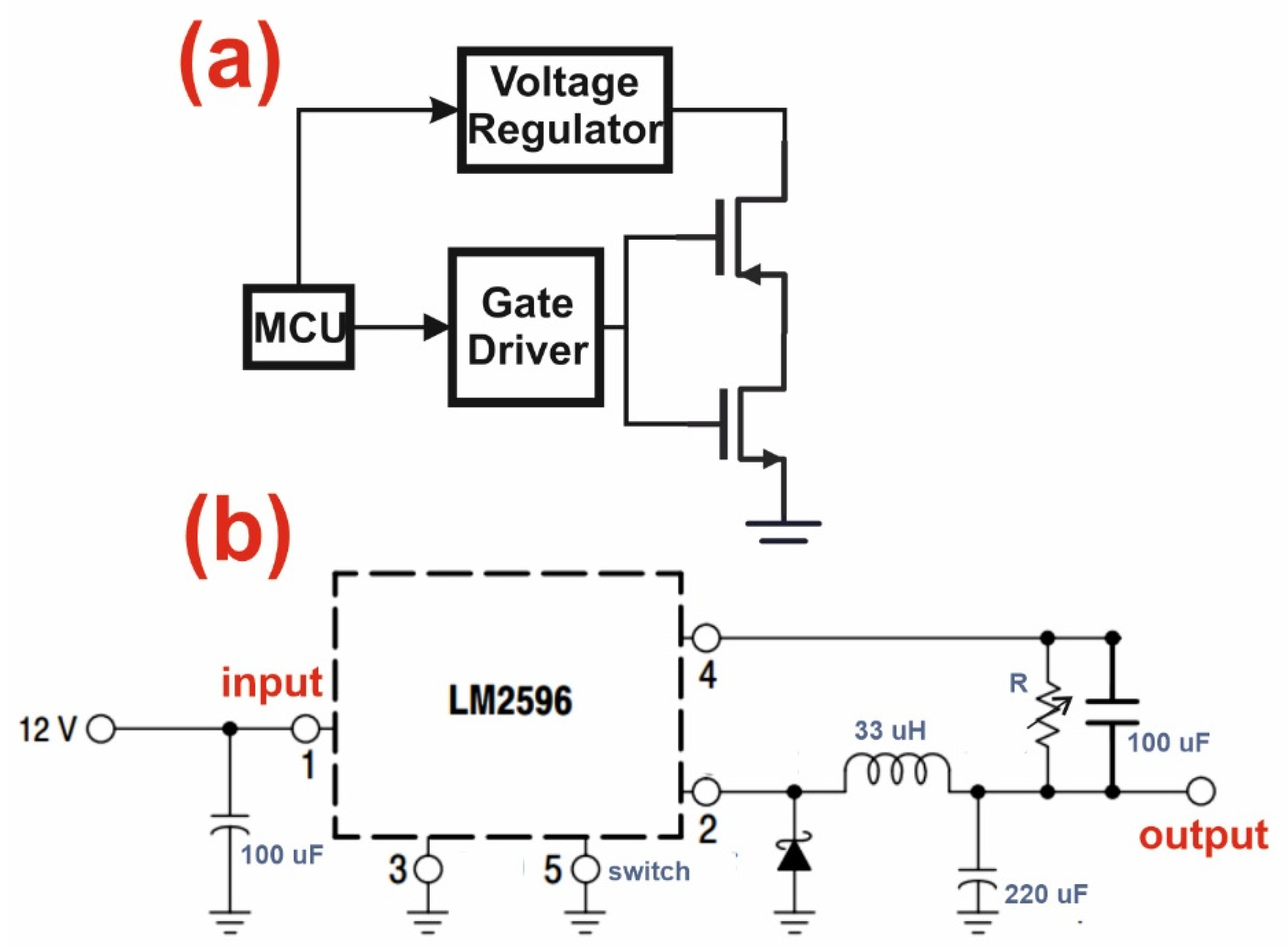
Figure 2a presents the three main parts of an inductive power transmission system. It consists of an oscillator controlled by a Microcontroller Unite (MCU), power amplifier, inductive link, rectifier, and load [22,23,24]. Optimization of the induction link requires making several trade-offs on the size aspect ratio, the distance between coils, and the coordinating misalignment between coils. Key elements of this optimization are coil parameters including size, width, and quality factors, as well as inductive link factors such as using intermediate resonator coils, connecting the external coil configuration, and reducing misalignment techniques [25]. To obtain a better view of efficiency optimization, the circuit model of the link is observed. For inductive WPT applications where the coil size is much smaller than the wavelength of the fields, distributed-element models are not required. Therefore, the induction coil is modeled according to Figure 2b. Parasitic and other elements in this model are derived from PCB coils. In this model, inductance (Ls) indicates the ability of the coil to store electromagnetic energy and is obtained by Equation (1) [26].
L s = 0.8 a 2 n 2 6 a + 9 b + 10 c
where a is the average internal and external radius, b is the height, c is the thickness of the coil along the radius, and n is the number of revolutions per layer. The intrinsic parallel capacitor (Cp) is determined by the spacing between planar conductive traces and their surrounding materials. PCBs are implemented on organic, ceramic, or silicon substrates and coated by an insulator, such as Perylene or silicone. In bioelectronic applications, coils are surrounded by tissue and fluids that have high permittivity. This causes an increase in the parasitic capacitance of the PSCs compared to when coils are in free air. The intrinsic parallel capacitor can be expressed by Equation (2) [27].
C P = C e x t l c
where lc is the PCB conductor length and C’ext is the capacity per-unit length obtained for the PCB coil and the surrounding materials such as tissues, the PCB substrate, the PCB coating, and air. The frequency at which the inductance (Ls) and intrinsic parallel capacitor (Cp) cause resonance is called the Self-Resonant Frequency (SRF) and is found by:
S R F = 1 2 π L s C p
In inductive design, the SRF frequency is usually higher than the ISM band (Industrial, Scientific, and Medical band), and to avoid interference, the resonance frequency of the circuit must be much smaller or equal to SRF [28,29]. The series resistance (RS) is a model of the losses that occur in the conductor of the coil. The skin and proximity effect at higher frequencies cause the conductor resistance and losses to increase with frequency. The skin effect increases the AC resistance of the coil at high frequencies [27]. At a frequency of zero, a uniform current density flows through the conductor, but as the frequency increases, the current density is large near the surface of the conductor and decreases exponentially with greater depths in the conductor. The current flows mostly in the skin of the conductor. The skin is the outer surface of the conductor and its depth, which depends on the current frequency. In other words, as the frequency increases, the effective current decreases and the conductor resistances increase [30]. The series resistance RS is calculated by applying Lenz’s law and considering the Eddy Current according to Equation (4).
  R s = R D C ( t 0 δ ( 1 e t 0 δ ) × 1 1 + t 0 w + 1 10 ( ω ω c r i t ) 2 )
where t0 and w are the conductor thickness and width, respectively. RDC is the zero-frequency conductor resistor, δ denotes the skin thickness, and ωcrit is the critical frequency of the proximity effect. The parallel resistor (Rp) models the loss of dielectric layers occurring at the power transmission site. Dielectric losses can be described by the loss tangent of each material’s tan (δ), which is related to its conductivity σ = ε 0 ε r ω tan   ( δ ) . ε 0   and   ε r are the permeability of the free space and material, respectively. Rp is the sum of material conductivity in the multilayer material such as in Figure 2d. In the model introduced in Figure 2b, the quality factor (Q) of a coil defines the ratio of energy stored to energy lost. To achieve a high-quality factor coil, the RS must be kept as low as possible.
Considering the quality coefficient as a result of the series resistance (QS) and the quality coefficient as a result of the parallel resistance (QP), the total quality coefficient can be calculated by Equation (5) [31].
Q = ( 1 Q s + 1 Q P ) 1 = ( R s L s ω + L s ω R P ) 1
In the induction link, the external coil produces a time-variant magnetic flux. Part of this flux passes through the space occupied by the internal coil and generates the voltage according to Faraday’s first law. Mutual Inductance (M) represents the ratio of the flux passing through the internal coil to the excitation current of the external coil. Mutual Inductance for the two coils with one wire loop can be calculated by Equation (6) [28]. Note that for coils with a high number of turns (i.e., n > 1), the sum of the M values at each turn must be calculated.
M = μ 0 π a 2 b 2 2 ( a 2 + b 2 + z 2 ) 3 / 2
where μ0 is the vacuum permeability and a and b are the coils’ radius. Furthermore, z is the coil spacing parameter. According to [28], the induction link voltage gain PTE is calculated by Equation (7).
  P T E = K . n . Q 1 Q 2 α 2 + 1 α K 2 Q 1 Q 2 + α + Q 2
where K is the coupling factor, n is the number of coil turns, and Q1 and Q2 are quality factors due to the external and internal coils, respectively. In Equation (7), α is a dimensionless parameter and depends on Cp as well as the load resistance. To obtain the maximum power transfer, we extract the alpha value for which Equation (7) is maximized. Therefore, to gain the maximum efficiency, the term K.Q1.Q2 must reach the maximum value [28]. The coupling factor is related to the mutual inductance by M = K sqrt (L1L2). Thus, provided that L1 and L2 remain unchanged, K reaches the maximum when M takes its highest value. As mentioned in Equation (6), M is dependent on the coil geometry. A crucial parameter of the M value is the distance between two coils, which reduces the M proportional to 1/z2. With regard to Q1 and Q2, a key factor in their values is the parasitic resistance Rs and p of both coils in the link, which should be kept as low as possible to preserve high Q as shown in Equation (5). To obtain a low RS, according to Equation (4), the wire thickness (c) with respect to the width (b) must remain low. With all these considerations, the coils with high-efficiency power transfer are designed in Section 3.2.

3. System Design

In this section, we use the relations for the coil parameters mentioned in Section 2 to design and optimize an array of coils. Two configurations of an array, a non-overlapped array and an overlapped array, are designed for maximum power transfer over a large area of an internal moving coil. According to the schematic presented in Figure 2a, first, a Class D amplifier is used to achieve low input impedance and high efficiency. In addition, there exists a microcontroller in this part that is responsible for determining the reference voltage of the Class D amplifier. It also is responsible for directing and controlling the current generated by the amplifier and excitation of the nearest transmitter coil to the receiver with a square pulse of an appropriate frequency. This frequency is selected to detect the maximum movement speed of a moving object and control the transmitter’s external coils’ excitation. This technique eliminates the need to transfer power to all external transmitter coils at the same time and thus leads to a reduction in power consumption. In part II (inductive link), eight array coils were designed in the external transmitter and one coil in the internal receiver. In part III, a full-wave diode rectifier and a smoothing capacitor are used to combat fluctuations in the voltage signal. An ohmic load on the rectifier output was used to evaluate the system performance.

3.1. System Performance Algorithm

The inductive WPT system operating mechanism is as follows: First, the amplifier is turned on by connecting it to the DC power supply. Second, by using the feedback mechanism, the position of the moving object is determined. The mechanism is such that when the internal coil is in the vicinity of an external coil in the array, it creates mutual coupling between the two coils. As a result, the current drawn from the amplifier connected to the external coil increases. By detecting this current and comparing it with the previous state, the microcontroller detects the current position of the internal coil. Therefore, MCU stops positioning the internal coil and excites the aforementioned external coil. This algorithm continues until the object moves to another position and the current drawn from the PA decreases. Therefore, the positioning algorithm starts again. After tracking the internal coil, the neighboring external coil(s) must be excited. A weak signal of the oscillator at the interested ISM frequency is generated for the amplifier transistor (i.e., part 2 in Figure 2a). Then, this weak signal is amplified by PA and excites the aforementioned coil(s). Third, after a time interval of approximately 1 ms, the algorithm repeats the second step to track the internal coil. Fourth, the link transfers the power to the moving object. Finally, the received power is rectified and converted to DC for the ohmic load. The PTE is measured at the load with uniformly received power versus an un-stationary internal coil.

3.2. Coil Design

According to Equation (7), improving the coil’s quality efficiency and amplifying the coupling factor cause an improvement in link efficiency. The inner (ID) and outer (OD) diameters, which are two of the most fundamental geometry parameters of coils, were examined. Six different coils with different IDs and turns were fabricated, and their parameters were measured. Measurements were performed using the GW INSTEK LRC meter 8000G series. According to Equation (4), the size of the coils has an impact on Rs, and according to Equation (5), Rs reduces the coil quality factor. There is a tradeoff between ID, turn number (n), spacing between turns (S), and the number of wires in the coil to achieve maximum quality factor and PTE. The measurement results are presented in Table 1. Based on the quality factor (Q) calculated in Table 1, the second coil was selected. The coil wire width was increased from 17.5 µm to 70 µm to achieve maximum Q (Equation (5)). In the coil wire with a width of approximately 70 µm, Q = 50.13 was recorded. So, this coil was tested in this research as the final coil, and 9 coils were fabricated with the mentioned specifications. Eight of them were used as external coil arrays in the transmitter and one of them was used as an internal coil in the receiver. The coils were implemented on a printed circuit board (PCB) to avoid a mismatch in the array coils.
To obtain matching impedance between the PA output and the input of the inductive link, a matching network is used with a lumped element LC network. To measure the input impedance of the coil, a Network Analyzer was used, and the impedance component, Z11, which indicates the input impedance of the coil array, is measured. The phase and magnitude of Z11 are shown as a function of frequency in Figure 3. Figure 3 shows the amplitude and phase of the input impedance of the inductive link Z11 with the frequency sweep. As shown in Figure 3, the ANSYS simulation and Network Analyzer measurement (inset image in Figure 3) results are consistent and show impedance of 48.5 Ω ∠ 86.3° at a working frequency of 900 kHz. By adding the matching network (a serial 27 pF capacitor and a 450 nH parallel inductance), the input impedance matches, and at a working frequency, 50 Ω impedance is observed. It can be seen that the coil input impedance at the working frequency reaches the maximum when its input reactance almost vanishes.
As the external and internal coils are the same size, the coupling factor is stronger rather than in the case where the coils have different sizes. That is because, in larger external coils, as the internal coil is displaced from the center of the external coil (see Figure 1), the electromagnetic field distribution at bigger coil borders drops sharply. Here we use an array composed of four coils as external power transmitter coils. In this case, the electromagnetic field vector at the border of two neighboring coils is the result vector consisting of two horizontal and vertical field vectors. The horizontal field is canceled out because the external coils are the same size, and the direction of the field is opposite at the boundaries. So, only the field remains in the vertical direction. Therefore, the resulting magnetic field at the borders is much weaker than the fields at the center of each coil. The amplitude of the magnetic field above the center of the transmitter coil is greater than in the other positions. This change in the number of fields in the vertical direction is due to the change in angle (the angle between the center line of the transmitter coil and the receiver position). In blank spots, the angle increases and the field amplitude is reduced (cosine relation) until it is re-amplified via the next transmitter. Therefore, to obtain a uniform field distribution for the application of a free-moving object, we investigate the 50% overlap of coils for a uniform field distribution.
Figure 4a shows the fabricated coil arrays’ configuration. The external array with eight coils consists of two sets of four-coil-plate arrays, which are placed with 50% overlap by shifting one plate in the x-direction. The second four coils are placed at an identical distance along the z-axis as the first plate is. However, the former is displaced by 25 mm along the x-direction (half of the square width) with respect to the first array. In each four-coil array plate, the coils are placed with no overlap. Furthermore, a multilayer capacitor is used for each coil for tuning at the resonance frequency.
This overlapped array coil structure removes blank spots created at the border of two neighboring coils. As shown in Figure 4b, in case coil arrays are on the same plate, points X1, X2, and X3 are considered blank spots. However, if the coil array is placed on two plates of an array that is shifted relative to each other, it causes the blank spots to disappear due to additional fields. Therefore, this causes a more uniform H field distribution along the direction of the internal coil, as depicted in Figure 4c.
In Figure 4b, the resultant fields of all coils in X1 are mainly due to the contribution of coils 1 and 2. This is because other coil fields drop sharply at the outer-center points. Additionally, for coils 1 and 2, point X1 is assumed to be an off-centered point and the fields drop sharply. When an overlapped plate is added to another array plate (see Figure 4c), the blue middle coil increases the field in the X1 position in a way that the overall fields are equal to the fields on top of coils 1 and 2. This provides more uniform fields above the array as the internal coil moves.

3.3. System Operation

The MCU shown in Figure 2a is an STM32F103 microcontroller that is used in the transmitter part. This microcontroller issues control signals. A square pulse with a frequency of 900 kHz and a Pulse Width Modulation (PWM) of 50% is generated by the microcontroller and gate driver to excite the PA switch. The dead time of the gate driver for PA switches is 13.8 ns as the microcontroller works with a 72 MHz oscillator.
An important application of the microcontroller is to find the position of the moving internal coil. The microcontroller first connects to each external array coil sequentially and measures the current flowing through them. The external coil with the larger current drawn shows that it is in the vicinity of the internal coil. This current is caused by mutual inductance between them. This mechanism is connected to each external coil and measures the coil current and then switches the PA to another coil in the array, and again, the current is repeated every 1 ms by the microcontroller. This time is chosen according to the clock of the microcontroller and the fact that the moving object, here the internal coil, cannot change positions between the transmitter coils faster than this. Moreover, the value of the power of the Class D amplifier can be adjusted by the microcontroller. This is performed by changing the VDD voltage and using feedback from the internal coil.

3.4. Class D Amplifier and Rectifier Design

A Class D amplifier circuit was used to excite the external coils. It is composed of a half-bridge circuit as shown schematically in Figure 5a. A Dual-Power MOSFET Transistor IRF7106 was used for transistors Q1 and Q2. The voltage regulator produces a voltage between 5 and 12 volts by tuning R. R is a resistive divider at the output of the voltage regulator that varies with a digital potentiometer (MCP41010) to produce a regulated voltage. The amount of the potentiometer is determined digitally via a Microprocessor. LM2596 IC is used for the voltage regulator. The relation to the LM2596 IC output is given as Equation (8).
V o u t = V r e f ( 1 + R )
In the receiver circuit, a full-wave rectifier with a PMEG2010 diode and a 22 µF smoothing capacitor for ripple cancelation is adapted. Furthermore, a 100 Ω resistive load is used as RL, which is in accordance with the datasheet of CREE LEDs for optogenetic applications [5]. The PA Class D output impedance matches 100 Ω and remains unchanged at the input. The actual loading for transmitter coils is, however, much higher than 100 Ω.
When the internal coil couples to the external coil, the current sink from the PA transistors in Figure 5a is increased. This current is measured using a resistor in a series with PA transistors. This mechanism detects the position of the internal coil with respect to the external coil(s) with simple feedback. The microcontroller uses the switching mechanism and puts each one of the external coils at the PA output. Then it measures the current of NMOS transistors and feeds it back to the microcontroller. Based on the position of the internal coil and coupling mechanism, the microcontroller keeps one of the external coils in the circuit until the internal coil is displaced.

4. Results and Discussion

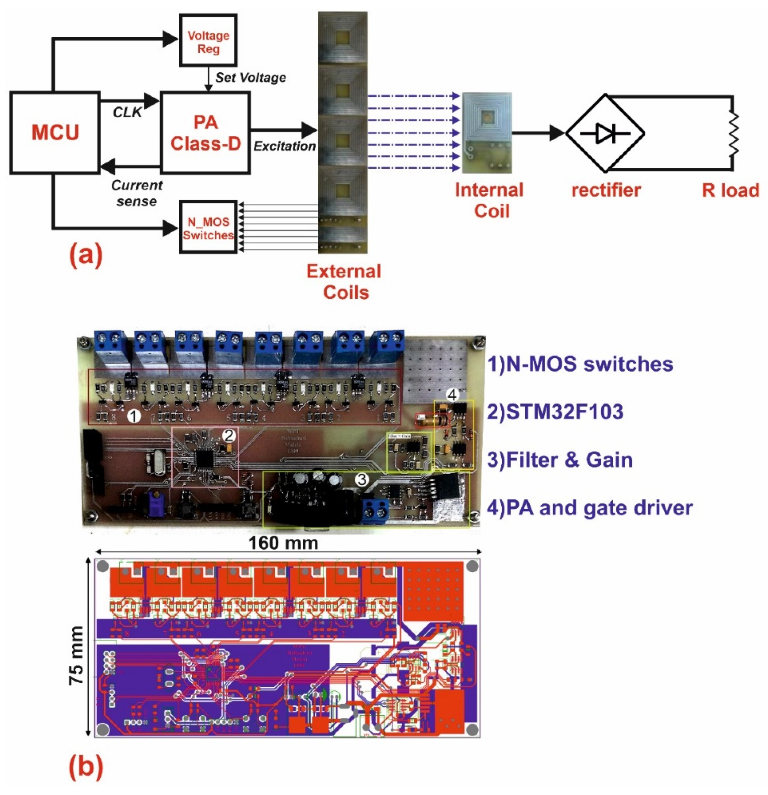
The two proposed overlapped array coils in the inductive WPT system are shown in Figure 6a. The microcontroller excites each external coil by the PA. The internal coil receives power from one of the external coils and transfers it to the rectifier. The rectifier converts the received signal from the internal coil to DC power and transmits it to the load. The two-layer PCB (double-sided PCB) is fabricated for the transmitted circuit as shown in Figure 6b. As can be seen, the main area of the PCB is dedicated to the NMOS Switch parts. Moreover, other parts of the transmitter circuit including the PA, gate drivers, gain, filters, and microcontroller are marked. The transmitter circuit is connected to the transmitter-tuned array via blue terminals on top of the PCB board. Furthermore, the micrograph of the PCB is shown in Figure 6b. The transmitter circuit area is 7.5 × 16 cm.
The voltage and current of fabricated circuits are recorded to measure the PTE of the inductive WPT system. The fabricated system shown in Figure 6b was connected to the designed external coil array (Figure 4a). The internal coil was connected to the ohmic load via a rectifier. The signal waveforms of the circuit were measured and examined using an oscilloscope.
The waveform voltage was measured at different nodes to investigate the performance operation of the circuit by a digital oscilloscope (GW Instek GDS-3000). Figure 7a indicates the PA voltages. The blue line shows the input voltage waveform of PA in the presence of an 82 Ω load in the receiver coil. The orange line shows the eight-volt voltage regulator (VDD). The RMS input current of the circuit was measured to be approximately 80 mA. The input of the PA is a pulse with an amplitude of approximately 10 V from peak to peak. To evaluate the performance of the output rectifier, the voltage waveform was measured at the input and output nodes of the rectifier. Figure 7b,c shows the input and output voltage of the rectifier in the no-load mode and with a load of 82 Ω. The blue line shows the input signal sent to the rectifier and the orange line shows the DC voltage delivered to the load. In the presence of an 82 Ω load, the output voltage was measured at approximately 6 V. The output current was recorded in the presence of 73 mA. By calculating the power at the regulator output and load input, an efficiency of 68% was obtained for the proposed inductive WPT.
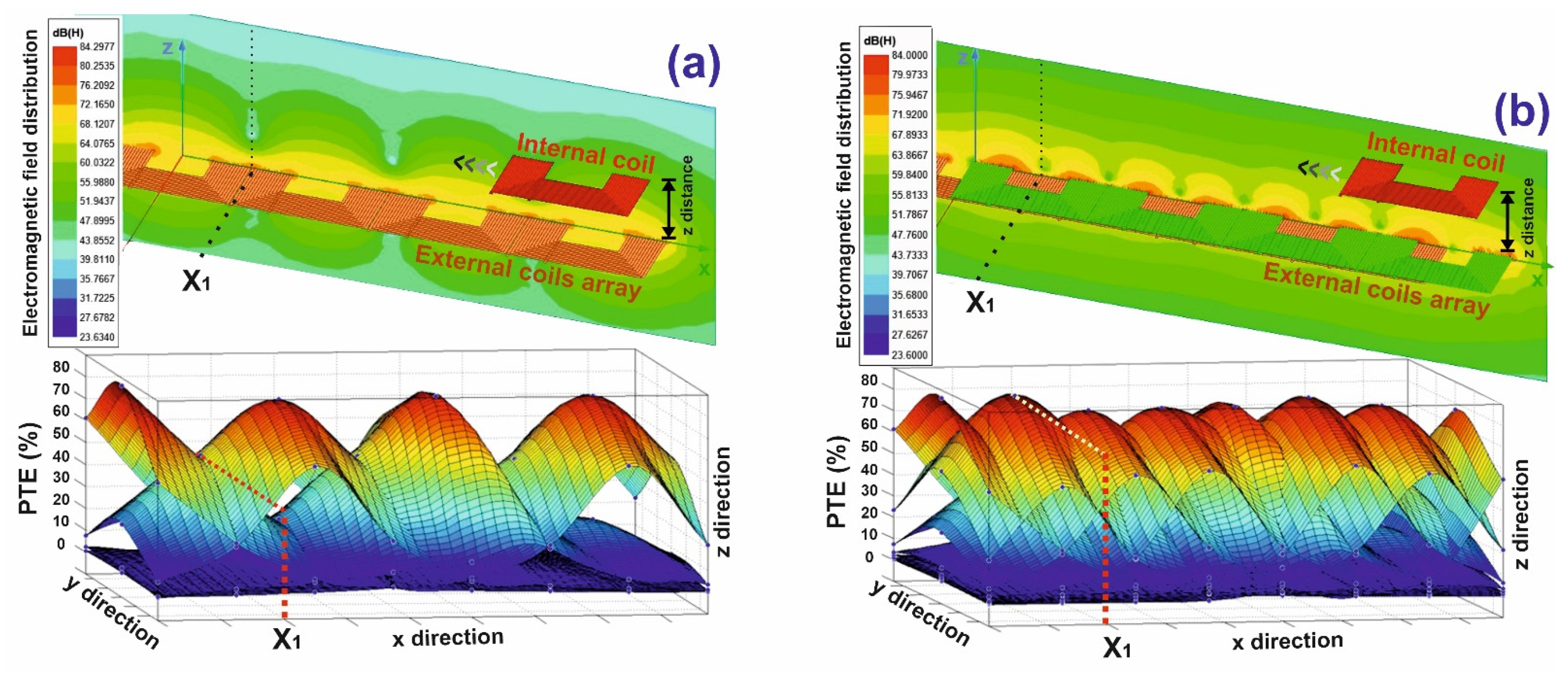
Figure 8 shows the electromagnetic field distribution and power transfer efficiency for both overlapped and non-overlapped structures. Simulation is verified by the Ansys HFSS 3D electromagnetic (EM) simulator at the working frequency (900 kHz). The moving internal coil moves at a distance of Z = 4 cm above the external array coils. Based on the top plot of Figure 8a, the electromagnetic field for moving the internal coil at blank spots (such as the X1 point) is cyan, which is in the range of 39–43 dB according to the color bar. Meanwhile, in the top plot of Figure 8b, it increased to lawn green color showing a range of 55–59 dB at both blank and other spots and maintained uniformity of the field distribution. Furthermore, PTE distributions are shown for overlapped and non-overlapped structures in Figure 8. As shown in the bottom plot of Figure 8a, the power measurement for non-overlapped structure variation is approximately 50% on top of the first external coil to the blank spot (X1) while the internal coil moves along the x-direction. When the internal coil starts to move, the internal and external coils are not necessarily co-axial. The coupling factor decreases when the receiver coil moves away from the center of the transmitter coil. Decreasing the coupling factor affects the system performance in three ways: (1) Load matching conditions are disruptive, (2) the link voltage gain changes, and (3) the load seen from the initial side of inductive WPT changes and reduces the efficiency of PA and changes the voltage of the coil.
PTE for the overlapped structure is measured in the bottom plot of Figure 8b with more uniform PTE distribution variations of approximately 10% along the x-axis. This change led to a uniform distribution of the electromagnetic field at the junction of the coils. This helps deliver constant power to the internal coil along the entire x-axis.
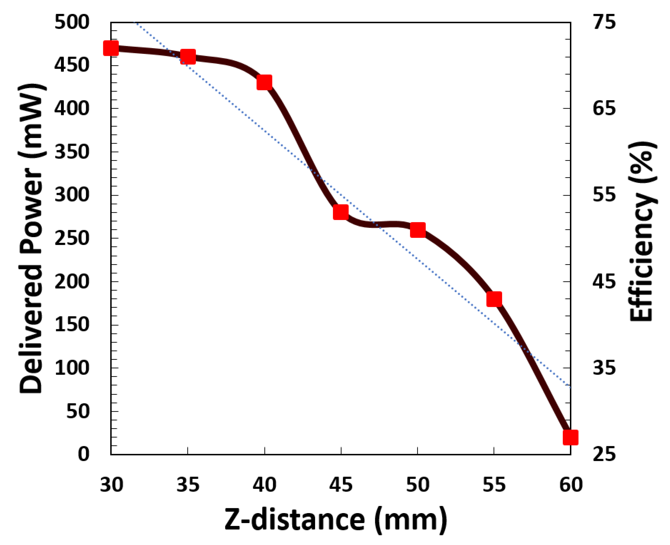
The effect of height changes in the range of 30 to 60 mm on the received power as well as the efficiency of the system was investigated. As shown in Figure 9, by increasing the distance between the internal and external coils, the delivered power and, consequently, the circuit efficiency decrease linearly. As depicted in Figure 9, point X was equal to 25 mm (X = X1 = 25 mm, the boundary between two coils on the first plate, see Figure 4). Changing the height of the moving coil in the overlapped configuration leads to a change in the received power, but as shown in the PTE distribution in Figure 8b, it does not disturb the uniform electromagnetic field in the x-direction.
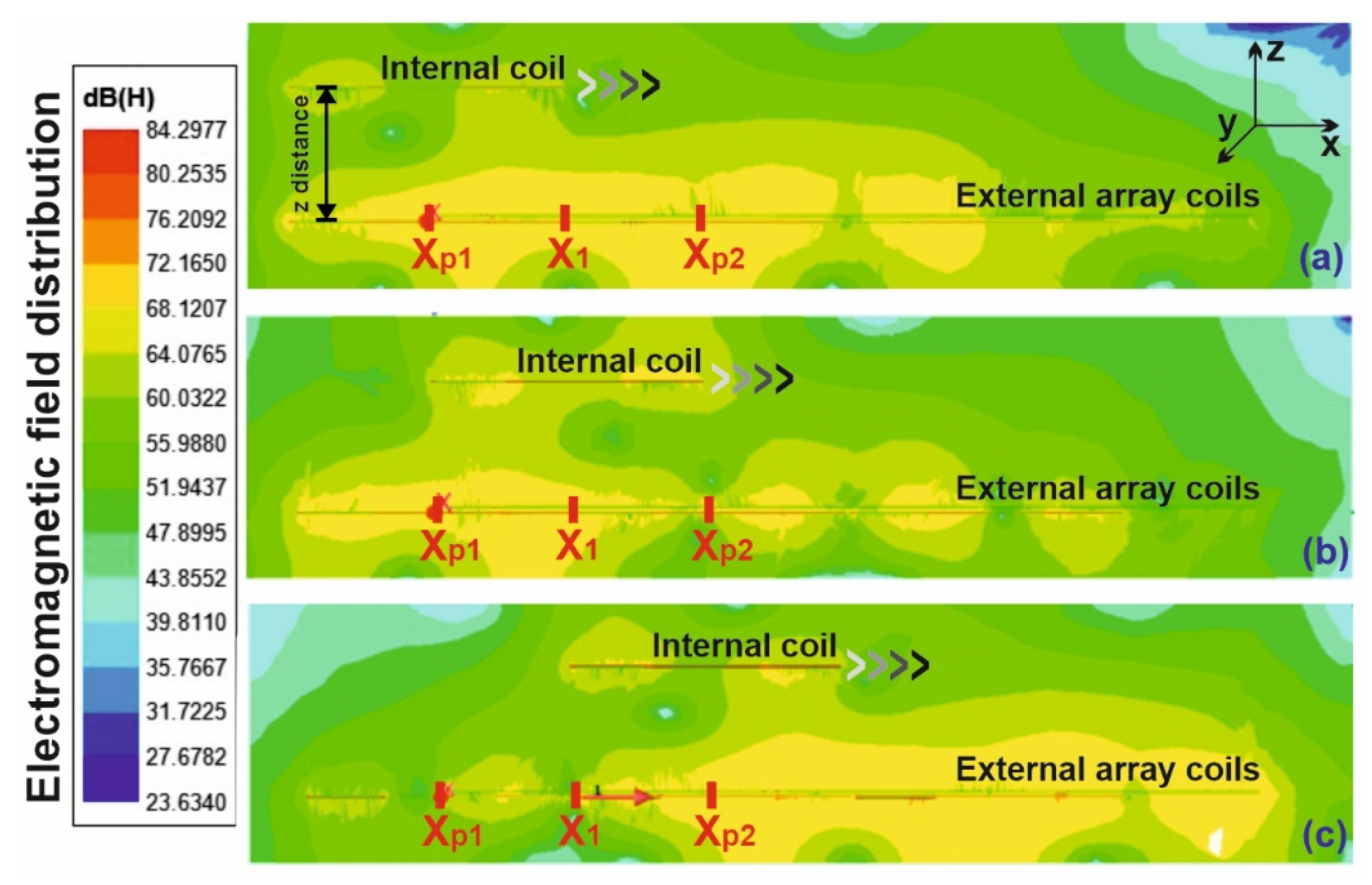
To evaluate the coding mechanism for tracking a moving object (internal coil), a test based on the movement of the coil was performed. In this test, the field distribution with internal coil movement from the top of the first external coil (Xp1) to the next coil (Xp2) was tracked as shown in Figure 10. The field intensity at each point indicates which external coil(s) is excited. This excited zone is shifted by the movement of the internal coil. As is shown in Figure 10, by changing the position of the internal coil from Xp1 to Xp2, only the external coils in the moving object’s neighborhood are excited. Therefore, they are coupled to the internal coil and the current flow in it. Furthermore, other external coils are in sleep mode. This mechanism helps to preserve some power consumption.
Furthermore, the power-saving mechanism does not affect the uniformity of the field distribution as depicted in Figure 10a–c. Even in the blank spot positions for the internal coil (X1) shown in Figure 10b, 68–72 dB was recorded for field distributions, the same as in Xp1 and Xp2.
Specific Absorption Rate (SAR) simulation results for biostability are shown in Figure 11. The simulation employed the ANSYS HFSSTM human model at 900 kHz (ISM band), for 1 W of input power. The SAR obtained at the working frequency, 0.115 mW/kg, is lower than the IEEE standard of 2 W/kg for 10 g of tissue [32].
Table 2 shows the main specifications of the proposed system. Moreover, this table provides the specifications of similar systems reported in the literature. It is clear that the power delivered to the load (PDL) as well as the power efficiency in this research is very significant. Meanwhile, the uniform electromagnetic field distribution and the removal of black spots were obtained in the present study. It should be noted that reducing the size of the coil decreases the system’s efficiency. Coils with smaller sizes can operate and deliver lower power because the smaller coil is exposed to fewer lines of the electromagnetic field. For internal coils with dimensions of 10 × 10 cm, the delivered power and efficiency were recorded as 266 mW and 41%, respectively. Table 2 summarizes the performance of the WPT system compared with the state of the art using the FOM introduced in [33], which uses the following parameters: The separation distance between the external and internal coils (d); the size of the external excitation coil array; the size of the internal coil; and the PDL and the PTE of the system. As shown in Table 2, the performance of the presented system is among the best-reported results. Using non-overlapped and overlapped coils in this system improves the PTE uniformity and illuminates blank spots. Furthermore, the tracking feedback mechanism improves PTE.
With the increasing use and tendency of wireless applications, the need to create a uniform field along the path of the moving receiver is increased. For free-moving transmitter coil applications, especially in biomedical or other applications such as electric vehicles, having a uniform field distribution among all the variations in the target position with respect to transmitter coils is a challenge.
In this research, we proposed a uniform field distribution for a moving object by using an overlapped-coils array. We presented a tracking mechanism to reduce the power consumption by avoiding all external coils’ excitation simultaneously. This tracking is performed using feedback from the moving coil position. Moreover, to remove the blank spots created by array coil borders and the field’s non-uniformity, overlapping mechanics are proposed.
For further investigation of this research, designing a high-efficiency link using a high-quality coil design and adding a matching circuit for the internal coil are suggested. Moreover, it is expected that by expanding the array into two or three dimensions, the proposed WPT system becomes more practical. Furthermore, by using the optimal positioning technique with the MCU algorithm or using the camera, the system speed and efficiency will increase.

5. Conclusions

We introduced a novel, multi-resonator array structure for an inductive WPT configuration. We analyzed and compared two types of coil arrays for wireless charging including one plate array and two overlapped arrays. Experimental measurement and simulation results confirmed that the overlapped array approached a uniform electromagnetic field. The parallel overlapped array is simple to implement and provides full power transmission uniformity when used in a 25 mm structure shifting along the moving coil path. Furthermore, we examined the effect of the height and size of the internal coil on the delivered power and efficiency. Comparing this research with other studies, we were able to create a uniform field distribution for a moving object in addition to increasing the PTE.

Author Contributions

Conceptualization, S.P.; methodology, S.P.; software, S.P.; validation, S.P. and M.S.; formal analysis, S.P.; investigation, S.P.; resources, S.P. and M.S.; data curation, S.P.; writing—original draft preparation, S.P. and M.S.; writing—review and editing, S.P. and M.S.; visualization, S.P., M.S. and M.M.; supervision, S.J.A.; project administration, S.P. and M.S. All authors have read and agreed to the published version of the manuscript.

Funding

This research received no external funding.

Data Availability Statement

The data presented in this study are available from the corresponding authors upon reasonable request.

Conflicts of Interest

The authors declare no conflict of interest.

References

  1. Nguyen, M.T.; Nguyen, C.V.; Truong, L.H.; Le, A.M.; Quyen, T.V.; Masaracchia, A.; Teague, K.A. Electromagnetic field based wpt technologies for uavs: A comprehensive survey. Electronics 2020, 9, 461. [Google Scholar] [CrossRef] [Green Version]
  2. Haerinia, M.; Shadid, R. Wireless power transfer approaches for medical implants: A Review. Signals 2020, 1, 12. [Google Scholar] [CrossRef]
  3. Akram, M.A.; Yang, K.-W.; Ha, S. Duty-Cycled Wireless Power Transmission for Millimeter-Sized Biomedical Implants. Electronics 2020, 9, 2130. [Google Scholar] [CrossRef]
  4. Shooshtari, M.; Salehi, A. An electronic nose based on carbon nanotube-titanium dioxide hybrid nanostructures for detection and discrimination of volatile organic compounds. Sens. Actuators B Chem. 2022, 357, 131418. [Google Scholar] [CrossRef]
  5. Gutruf, P.; Krishnamurthi, V.; Vázquez-Guardado, A.; Xie, Z.; Banks, A.; Su, C.-J.; Xu, Y.; Haney, C.R.; Waters, E.A.; Kandela, I.; et al. Fully implantable optoelectronic systems for battery-free, multimodal operation in neuroscience research. Nat. Electron. 2018, 1, 652–660. [Google Scholar] [CrossRef]
  6. Schormans, M.; Valente, V.; Demosthenous, A. Practical inductive link design for biomedical wireless power transfer: A tutorial. IEEE Trans. Biomed. Circuits Syst. 2018, 12, 1112–1130. [Google Scholar] [CrossRef] [Green Version]
  7. Kanaan, A.I.; Sabaawi, A.M. Implantable Wireless Systems: A Review of Potentials and Challenges; IntechOpen: London, UK, 2021. [Google Scholar] [CrossRef]
  8. Alam, B.; Islam, N.; Subhan, I.; Sarfraz, M. Analysis and Modelling of Basic Wireless Power Transfer Compensation Topology: A Review. Intell. Data Anal. Power Energy Syst. 2022, 802, 501–515. [Google Scholar]
  9. Houran, M.A.; Yang, X.; Chen, W. Magnetically coupled resonance WPT: Review of compensation topologies, resonator structures with misalignment, and EMI diagnostics. Electronics 2018, 7, 296. [Google Scholar] [CrossRef] [Green Version]
  10. Zhang, Z.; Pang, H.; Georgiadis, A.; Cecati, C. Wireless power transfer—An overview. IEEE Trans. Ind. Electron. 2018, 66, 1044–1058. [Google Scholar] [CrossRef]
  11. Sampath, J.; Vilathgamuwa, D.M.; Alphones, A. Efficiency enhancement for dynamic wireless power transfer system with segmented transmitter array. IEEE Trans. Transp. Electrif. 2015, 2, 76–85. [Google Scholar] [CrossRef]
  12. Jia, Y.; Wang, Z.; Mirbozorgi, S.A.; Ghovanloo, M. A closed-loop wireless homecage for optogenetic stimulation experiments. In Proceedings of the 2015 IEEE Biomedical Circuits and Systems Conference (BioCAS), Atlanta, GA, USA, 22–24 October 2015; pp. 1–4. [Google Scholar]
  13. Xu, C.; Zhuang, Y.; Han, H.; Song, C.; Huang, Y.; Zhou, J. Multi-coil high efficiency wireless power transfer system against misalignment. In Proceedings of the 2018 IEEE MTT-S International Wireless Symposium (IWS), Chengdu, China, 6–10 May 2018; pp. 1–3. [Google Scholar]
  14. Zheng, W.; Xie, F.; Xiao, W.; Qiu, D.; Zhang, B. Plane-Omnidirectional Wireless Power Transfer System Based on Vector-Controlled Flux Linkage. IEEE Access 2021, 9, 105651–105666. [Google Scholar] [CrossRef]
  15. Basar, M.R.; Ahmad, M.Y.; Cho, J.; Ibrahim, F. An improved wearable resonant wireless power transfer system for biomedical capsule endoscope. IEEE Trans. Ind. Electron. 2018, 65, 7772–7781. [Google Scholar] [CrossRef]
  16. Gutruf, P.; Rogers, J.A. Implantable, wireless device platforms for neuroscience research. Curr. Opin. Neurobiol. 2018, 50, 42–49. [Google Scholar] [CrossRef] [PubMed]
  17. Rakhyani, A.K.R.; Lazzi, G. Apparatus, System, and Method for Multicoil Telemetry. U.S. Patent 9,368,273, 9 March 2012. [Google Scholar]
  18. Wei, X.; Wang, Z.; Dai, H. A critical review of wireless power transfer via strongly coupled magnetic resonances. Energies 2014, 7, 4316–4341. [Google Scholar] [CrossRef] [Green Version]
  19. Kim, J.H.; Choi, B.G.; Jeong, S.Y.; Han, S.H.; Kim, H.R.; Rim, C.T.; Kim, Y.-S. Plane-type receiving coil with minimum number of coils for omnidirectional wireless power transfer. IEEE Trans. Power Electron. 2019, 35, 6165–6174. [Google Scholar] [CrossRef]
  20. Liu, G.; Zhang, B.; Xiao, W.; Qiu, D.; Chen, Y.; Guan, J. Omnidirectional wireless power transfer system based on rotary transmitting coil for household appliances. Energies 2018, 11, 878. [Google Scholar] [CrossRef] [Green Version]
  21. Wang, W.; Zhu, Z.; Wang, Q.; Hu, M. Optimisation design of real-time wireless power supply system overhead high-voltage power line. IET Electr. Power Appl. 2019, 13, 206–214. [Google Scholar] [CrossRef]
  22. Pahlavan, S.; Ghaznavi-Ghoushchi, M. 1.45 GHz differential dual band ring based digitally-controlled oscillator with a reconfigurable delay element in 0.18 μm CMOS process. Analog. Integr. Circuits Signal Processing 2016, 89, 461–467. [Google Scholar] [CrossRef]
  23. Khan, S.R.; Pavuluri, S.K.; Cummins, G.; Desmulliez, M.P. Wireless power transfer techniques for implantable medical devices: A review. Sensors 2020, 20, 3487. [Google Scholar] [CrossRef]
  24. Rotenberg, S.A.; Podilchak, S.K.; Re, P.D.H.; Mateo-Segura, C.; Goussetis, G.; Lee, J. Efficient rectifier for wireless power transmission systems. IEEE Trans. Microw. Theory Tech. 2020, 68, 1921–1932. [Google Scholar] [CrossRef]
  25. Pérez-Nicoli, P.; Silveira, F.; Ghovanloo, M. Inductive Links for Wireless Power Transfer; Springer: Berlin/Heidelberg, Germany, 2021. [Google Scholar]
  26. Terman, F.E. Radio Engineers’ Handbook; McGraq-Hill Book Company Inc.: New York, NY, USA, 1943. [Google Scholar]
  27. Jow, U.-M.; Ghovanloo, M. Modeling and optimization of printed spiral coils in air, saline, and muscle tissue environments. IEEE Trans. Biomed. Circuits Syst. 2009, 3, 339–347. [Google Scholar]
  28. van Schuylenbergh, K.; Puers, R. Inductive powering: Basic theory and Application to Biomedical Systems; Springer: Berlin/Heidelberg, Germany, 2009. [Google Scholar]
  29. Bareli, S.; Geri, L.; Nikulshin, Y.; Nahum, O.E.; Hadas, Y.; Yeshurun, Y.; Yaniv, E.; Wolfus, S. Effect of Coil Dimensions on Dynamic Wireless Power Transfer for Electric Vehicles. TechRxiv 2021. [Google Scholar] [CrossRef]
  30. Zhang, H.; Yao, M.; Kails, K.; Machura, P.; Mueller, M.; Jiang, Z.; Xin, Y.; Li, Q. Modelling of electromagnetic loss in HTS coated conductors over a wide frequency band. Supercond. Sci. Technol. 2020, 33, 025004. [Google Scholar] [CrossRef]
  31. Finkenzeller, K. RFID Handbook: Fundamentals and Applications in Contactless Smart Cards, Radio Frequency Identification and Near-Field Communication; John Wiley & Sons: Hoboken, NJ, USA, 2010. [Google Scholar]
  32. Bocan, K.N.; Mickle, M.H.; Sejdić, E. Multi-disciplinary challenges in tissue modeling for wireless electromagnetic powering: A review. IEEE Sens. J. 2017, 17, 6498–6509. [Google Scholar] [CrossRef]
  33. Maghsoudloo, E.; Gagnon-Turcotte, G.; Rezaei, Z.; Gosselin, B. A smart neuroscience platform with wireless power transmission for simultaneous optogenetics and electrophysiological recording. In Proceedings of the 2018 IEEE International Symposium on Circuits and Systems (ISCAS), Florence, Italy, 27–30 May 2018; pp. 1–5. [Google Scholar]
  34. Biswas, D.K.; Martinez, J.H.; Daniels, J.; Bendapudi, A.; Mahbub, I. A novel 3-d printed headstage and homecage based wpt system for long-term behavior study of freely moving animals. In Proceedings of the 2020 IEEE Radio and Wireless Symposium (RWS), San Antonio, TX, USA, 26–29 January 2020; pp. 268–271. [Google Scholar]
  35. Biswas, D.K.; Martinez, J.H.A.; Kaul, I.; Kaul, A.; Mahbub, I. A Miniaturized Highly Efficient Headstage Based Wireless Power Transfer (WPT) System for Optogenetic Stimulation of Freely Moving Animals. In Proceedings of the 2020 IEEE 14th Dallas Circuits and Systems Conference (DCAS), Dallas, TX, USA, 15–16 November 2020; pp. 1–4. [Google Scholar]
  36. Maghsoudloo, E.; Rezaei, M.; Gosselin, B. A wirelessly powered high-speed transceiver for high-density bidirectional neural interfaces. In Proceedings of the 2017 IEEE International Symposium on Circuits and Systems (ISCAS), Baltimore, MD, USA, 28–31 May 2017; pp. 1–4. [Google Scholar]
Figure 1. Schematic of inductive WPT system for (a) single external coil and (b) array external coil for free-moving object.
Electronics 11 01204 g001
Figure 2. (a) Schematic of inductive power transmission system. (b) Compact circuit model of a coil. (c) Coil size cross-section. (d) Multilayer model of PCB for parasitic elements.
Electronics 11 01204 g002
Figure 3. Impedance response of real and imaginary parts of Z11 of the fabricated coil vs. frequency.
Electronics 11 01204 g003
Figure 4. (a) Fabricated coil arrays. (b) Schematic of one plate array coil vs. electromagnetic field distribution. (c) Schematic of two overlapped plate array coils vs. electromagnetic field distribution.
Electronics 11 01204 g004
Figure 5. (a) Schematic of Class D amplifier. (b) Circuit designed to run the LM2596 IC.
Electronics 11 01204 g005
Figure 6. (a) The proposed inductive WPT setup using the two overlapped external coils with PA and rectifier. (b) Fabricated PCB and PCB layout of transmitter board.
Electronics 11 01204 g006
Figure 7. (a) Voltage regulator and PA waveform. (b) Input and no-load output voltage of rectifier. (c) Input and output voltage to the 82 Ω load of rectifier (shown in the schematic of Figure 6a).
Electronics 11 01204 g007
Figure 8. Electromagnetic field distribution and power transfer efficiency for (a) non-overlapped and (b) overlapped structures.
Electronics 11 01204 g008
Figure 9. Variation of delivered power to internal coil and system efficiency vs. height changes of internal coil (X position is fixed to 25 mm for all experimental).
Electronics 11 01204 g009
Figure 10. Electromagnetic field distribution over internal coil movement from (a) top of first external coil, (b) border of two neighborhood coils with a 50% overlapped coil, and (c) top of next neighboring external coil.
Electronics 11 01204 g010
Figure 11. 3D SAR for human head at 13.56 MHz For internal coil excited by overlapped external coil array. (a) SAR side view. (b) SAR top view.
Electronics 11 01204 g011
Table 1. Specifications of fabricated coils (OD is 50 mm, W is 1 mm, and Ctank is fixed to 680 pF).
Electronics 11 01204 i001 Electronics 11 01204 i002 Electronics 11 01204 i003 Electronics 11 01204 i004 Electronics 11 01204 i005 Electronics 11 01204 i006
ID (mm)281515151528
N8121314138
S (mm)0.350.250.350.250.350.35
Layer222211
L (μH)14.714.52326.76.44.1
RT (Ω)68910.5322.5
SRF (MHz)14.5714.414.2314.1715.3615.83
Q24.1714.719.7718.6931.63.24
Table 2. A comparison between the proposed system and similar studies based on the main specifications of the system.
SpecificThis Study[34][35][33][36]
Transmitter coil(s) size (cm)5 × 528.5 × 1820.7 × 1424 × 4650 × 60
Receiver coil size (cm)5 × 52.6 × 3.51.4 × 1.11.5 × 1.54 × 4
Array StructureYESNOYESYESYES
d (cm)4530–2012
PDL (mW)439133167420
PTE (%)6841.74929.419
Power transmission environmentairairairairair
FOM *2981220108218
* FOM = d × PTE × PDL × Size.
Publisher’s Note: MDPI stays neutral with regard to jurisdictional claims in published maps and institutional affiliations.

