
An Analysis and Modeling of the Class-E Inverter for ZVS/ZVDS at Any Duty Ratio with High Input Ripple Current


 , , , , ,
  , and
, and
Abstract
:1. Introduction
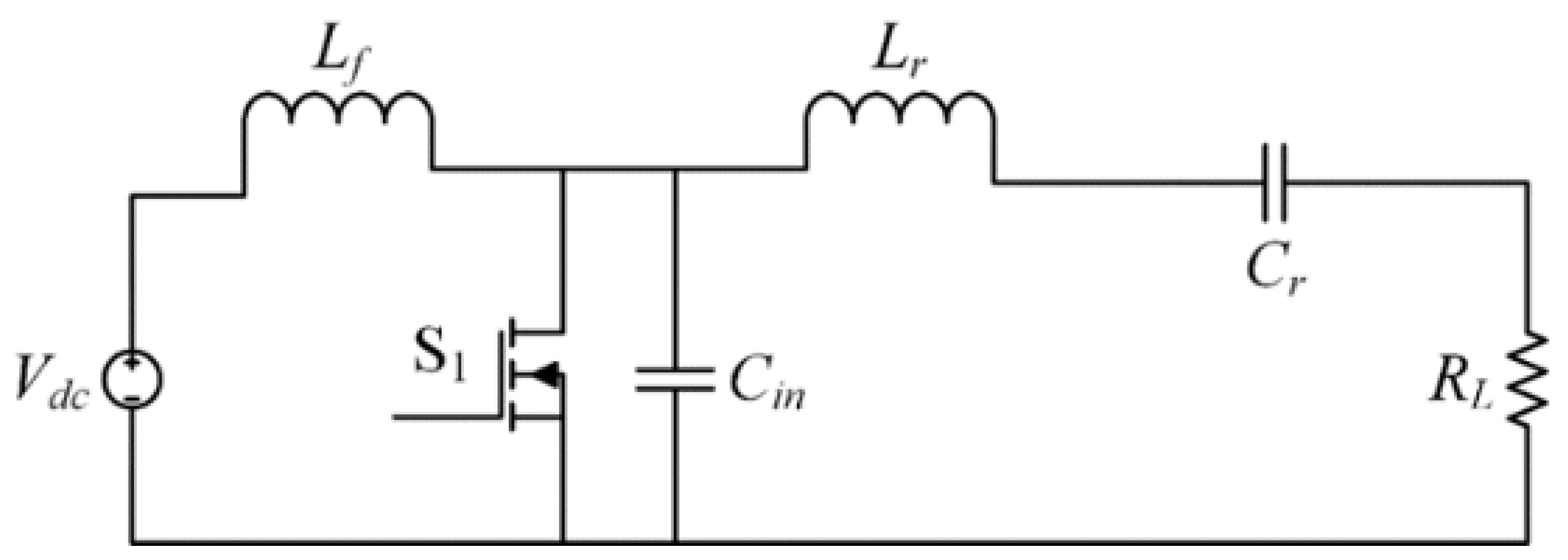
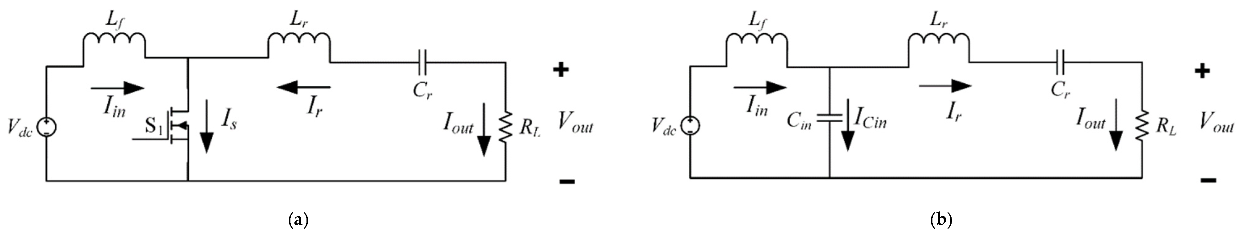
2. The Circuit Operation of Class-E Inverter
2.1. Modes of Operation
2.2. Assumptions
- All the components are ideal and do not possess any parasitic resistance or capacitances.
- The switch is ideal. It is an open circuit (vs = ∞) while OFF and shorted (vs = 0) while ON.
- The input current (Iin) is always positive.
3. The Circuit Modeling
3.1. Modeling Approach
- Step 1: To determine the switch voltage (vs(θ))
- Step 2: To apply the boundary conditions for ZVS/ZVDS and find input current (Iin(θ))
- Step 3: To find Lf_boundary and the input ripple current (Δiin)
- Step 4:
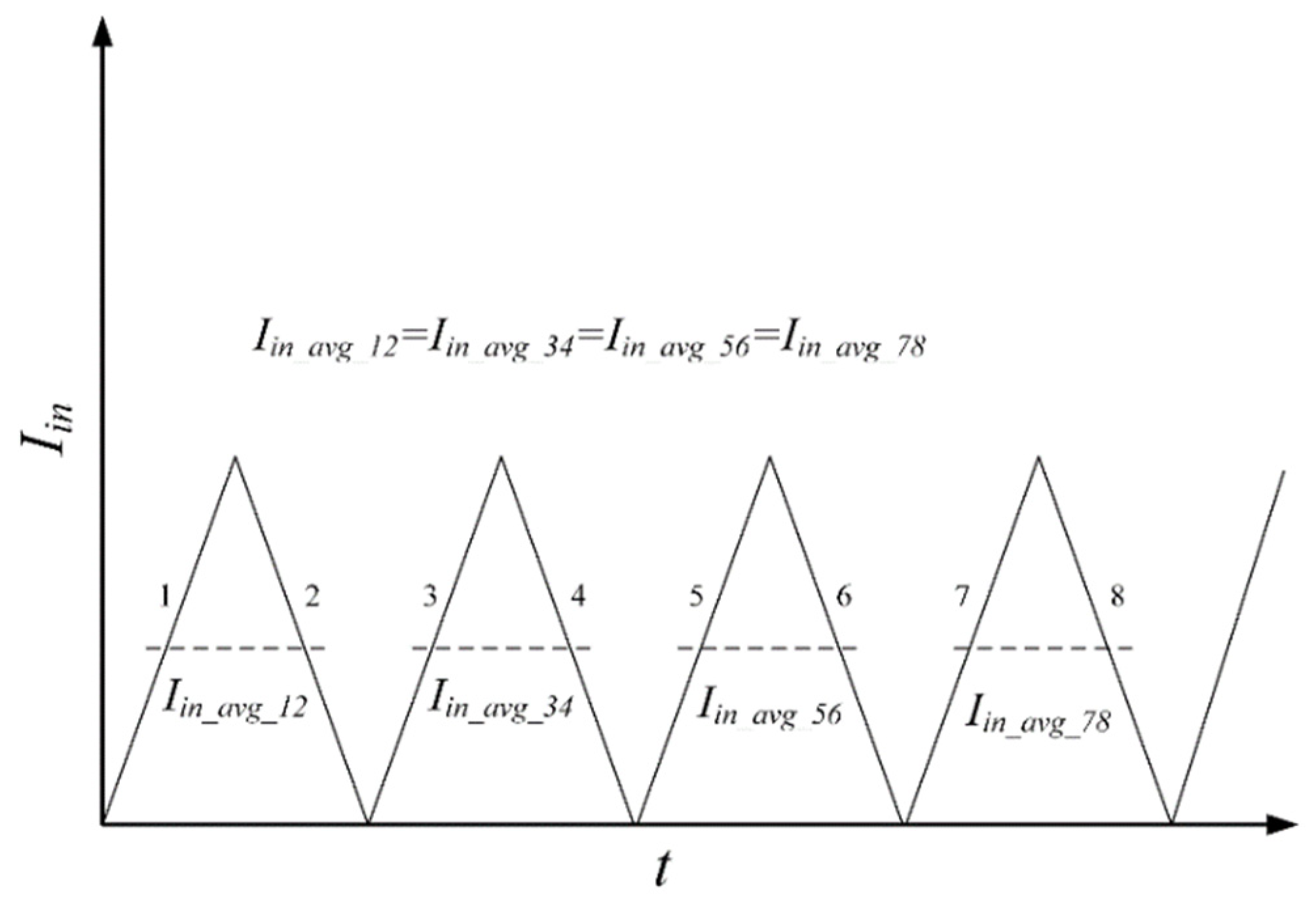
- Case 1 (N ≈ 1)
- (1)
- To determine the average input current (Iin_avg_case1)
- (2)
- Using Iin_avg_case1 to find the input capacitance (Cin_case1)
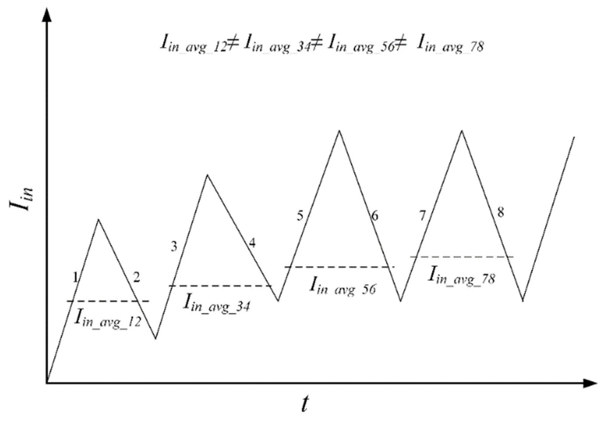
- Case 2 (1.5 < N < 3)
- (1)
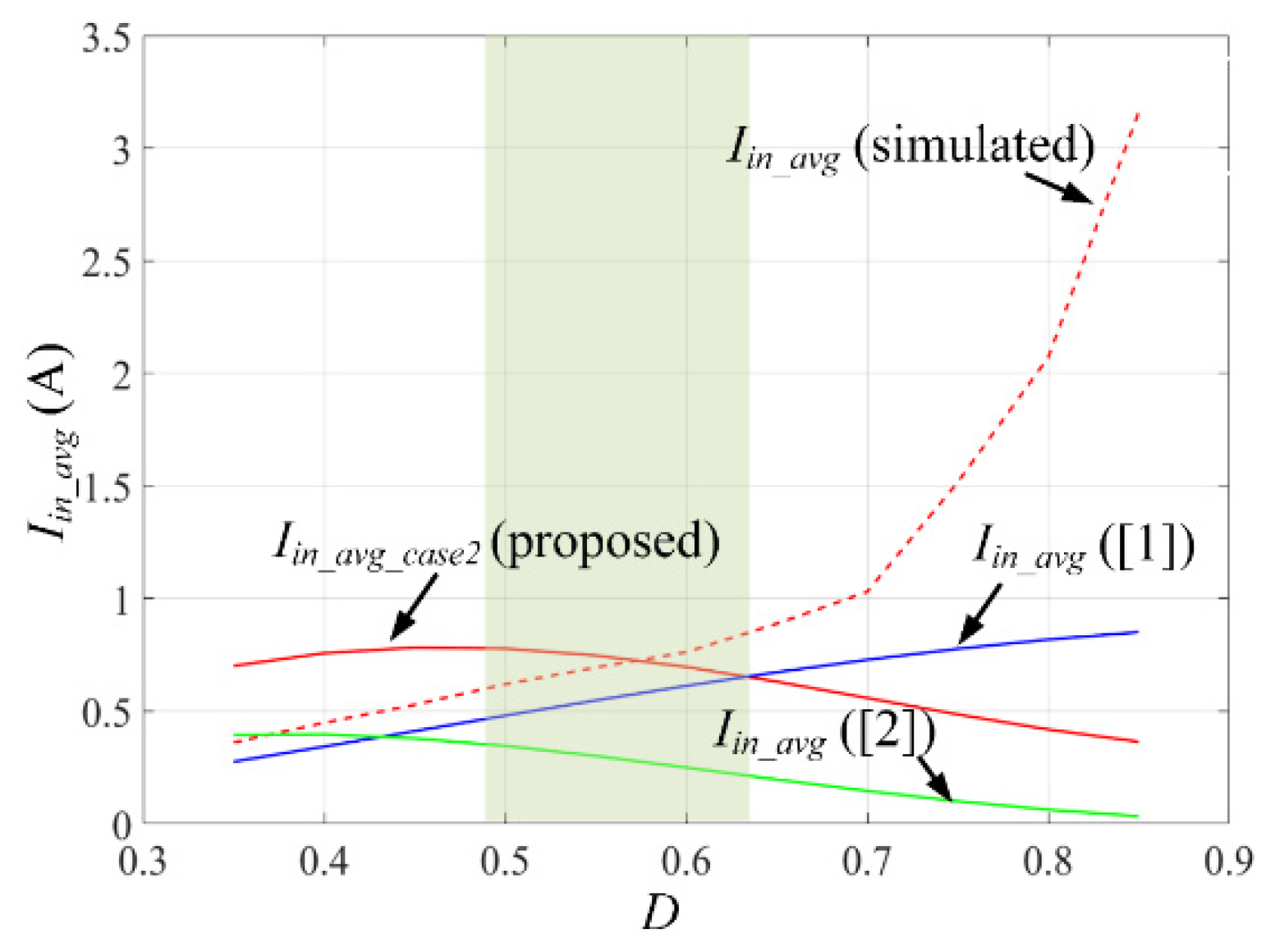
- To determine the average input current (Iin_avg_case2)
- (2)
- Using Iin_avg_case2 to find the input capacitance (Cin_case2)
- Case 3 (N ≥ 3)
- (1)
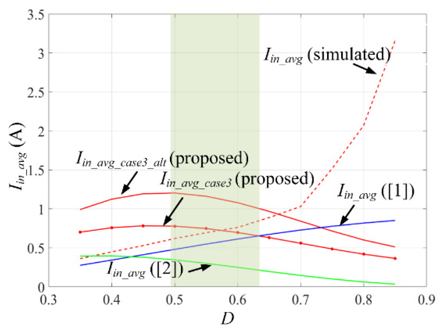
- To determine the average input current (Iin_avg_case3)
- (2)
- Using Iin_avg_case3 to find the input capacitance (Cin_case3)
- Step 5: To find the peak switch voltage (vs_pk) and the peak switch current (is_pk)
3.2. The Derivation
3.2.1. Step 1
- Ir(θ) is the resonant current;
- ICin is the capacitor current;
- Iin(θ) is the input current.
3.2.2. Step 2
3.2.3. Step 3
3.2.4. Step 4
- (a)
- Case 1: The input average current and the input capacitance for N ≈ 1
- (b)
- Case 2: The input average current and the input capacitance for 1.5 < N < 3:
- (c)
- Case 3-The input average current and the input capacitance for N ≥ 3:
3.2.5. Step 5
4. Analysis of The Model Parameters
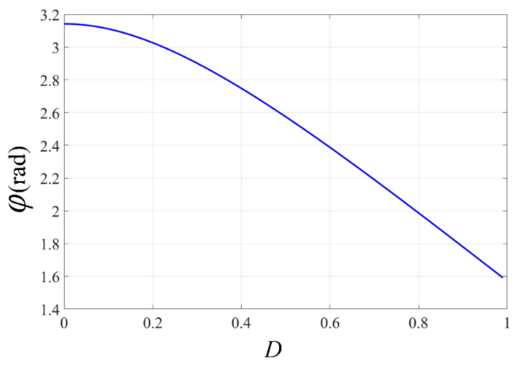
4.1. The Phase Difference (φ):
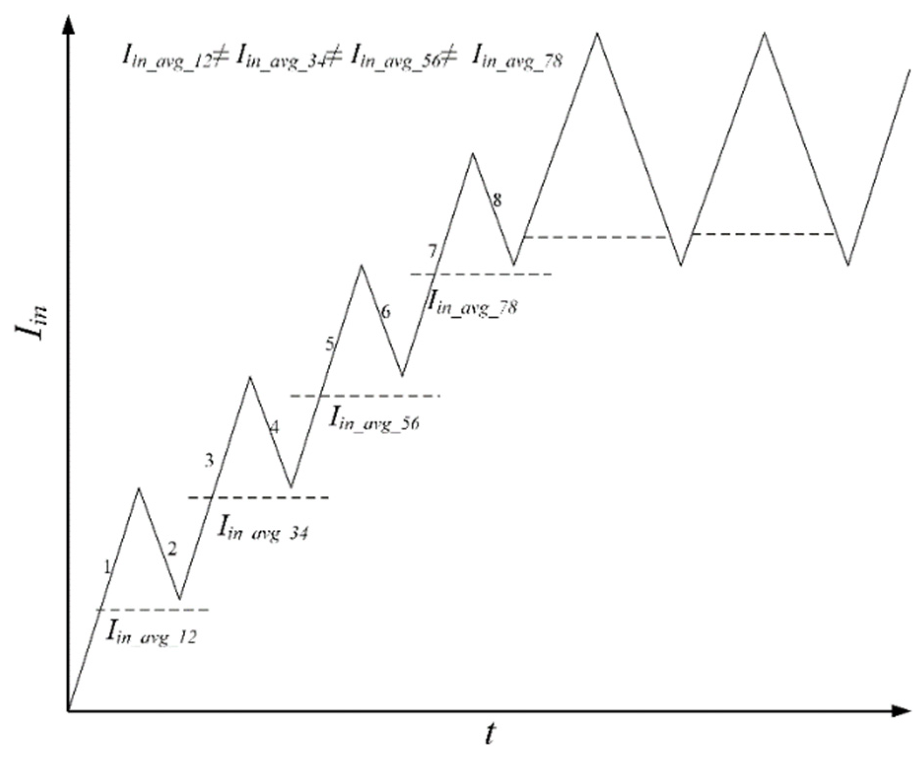
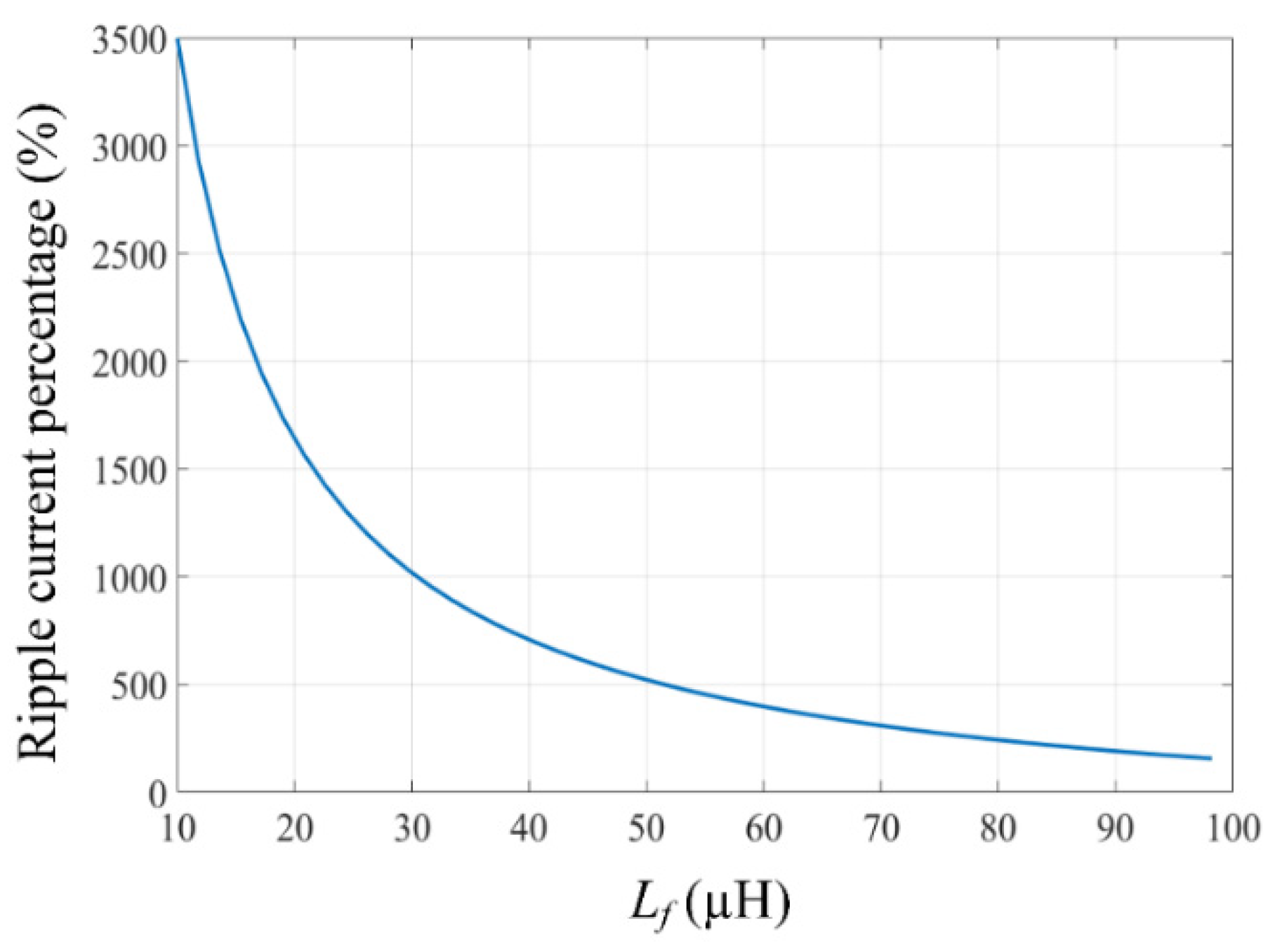
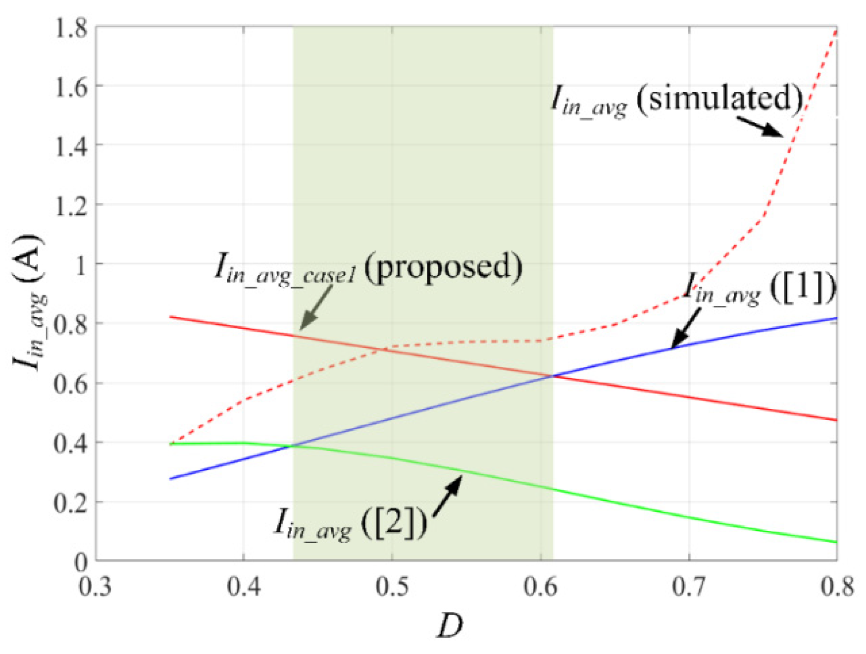
4.2. The Input Current Ripple
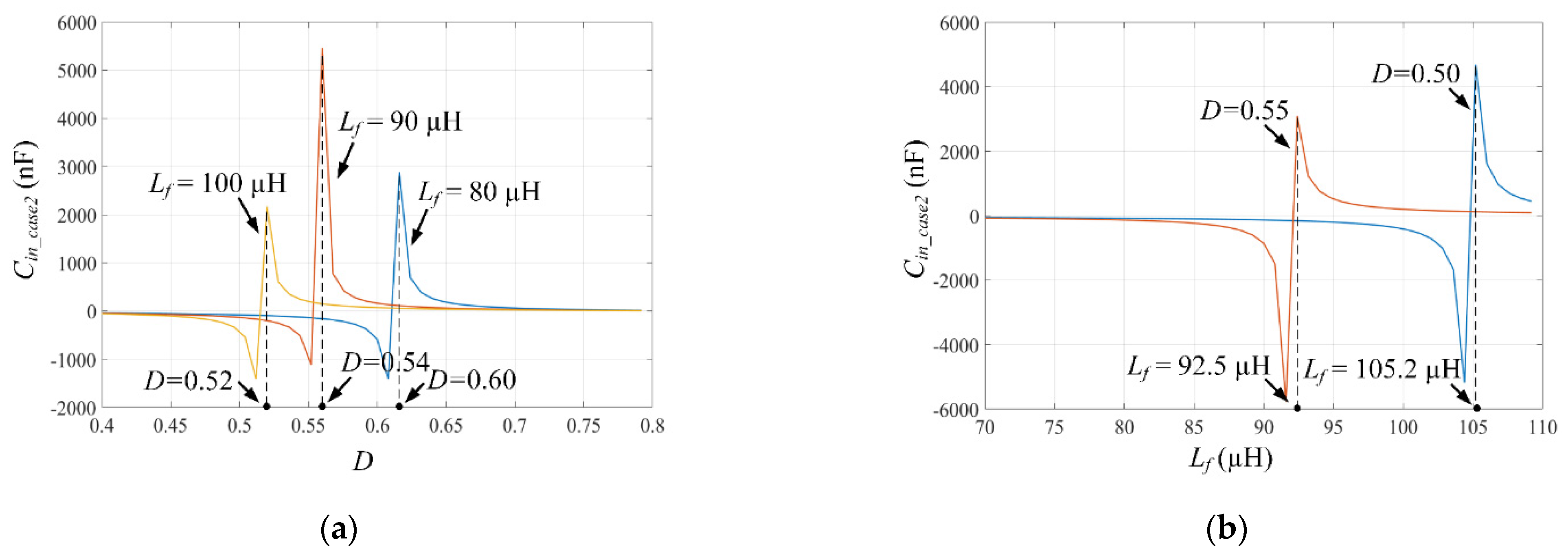
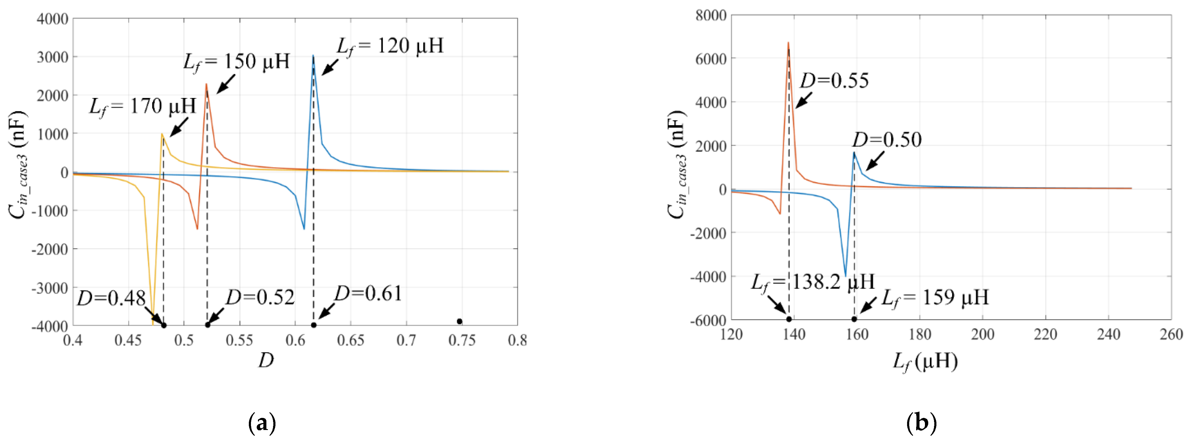
4.3. The Input Capacitance (Cin)
4.3.1. Case 1
4.3.2. Case 2
4.3.3. Case 3
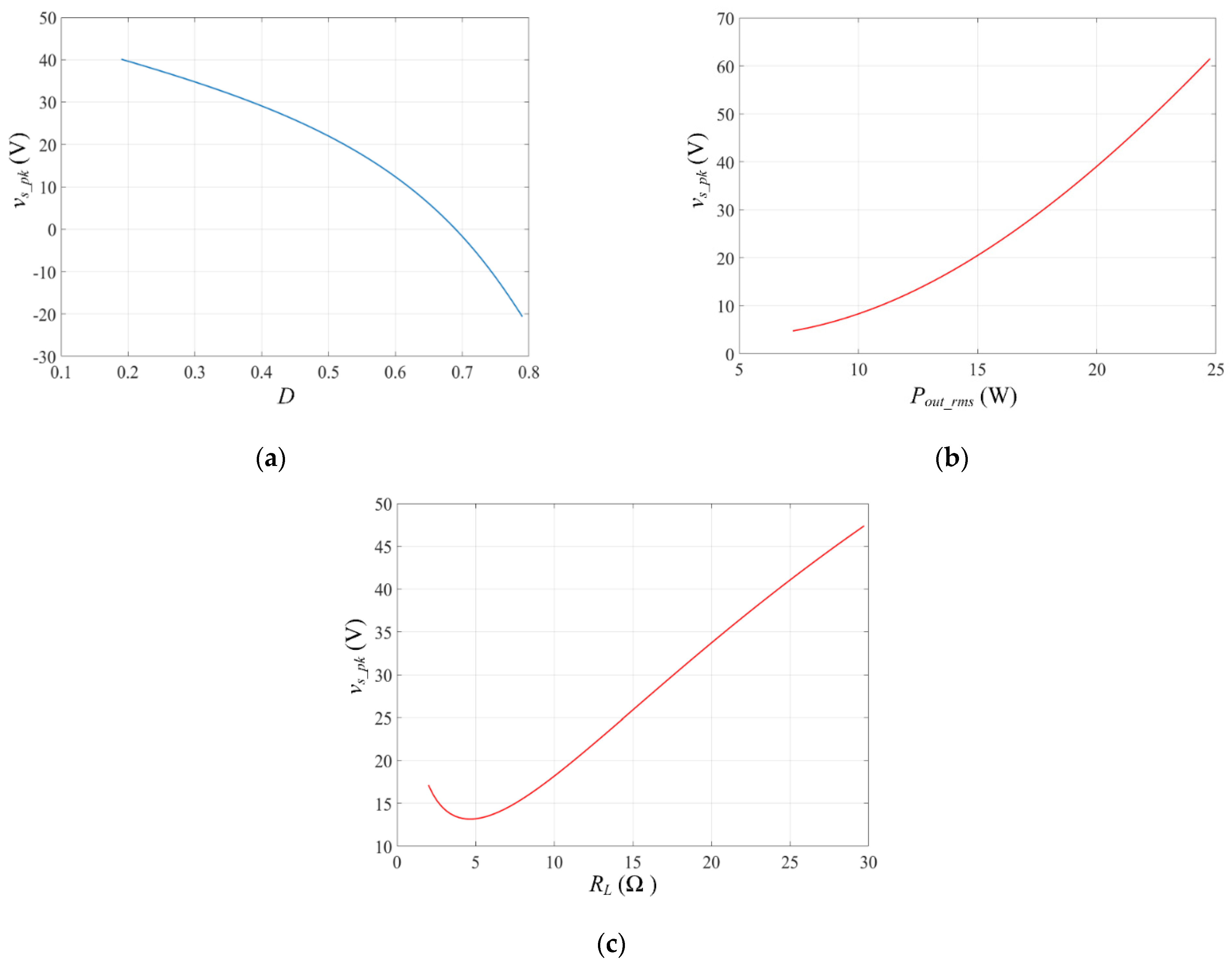
4.4. Peak Switch Voltage (Vs-pk)
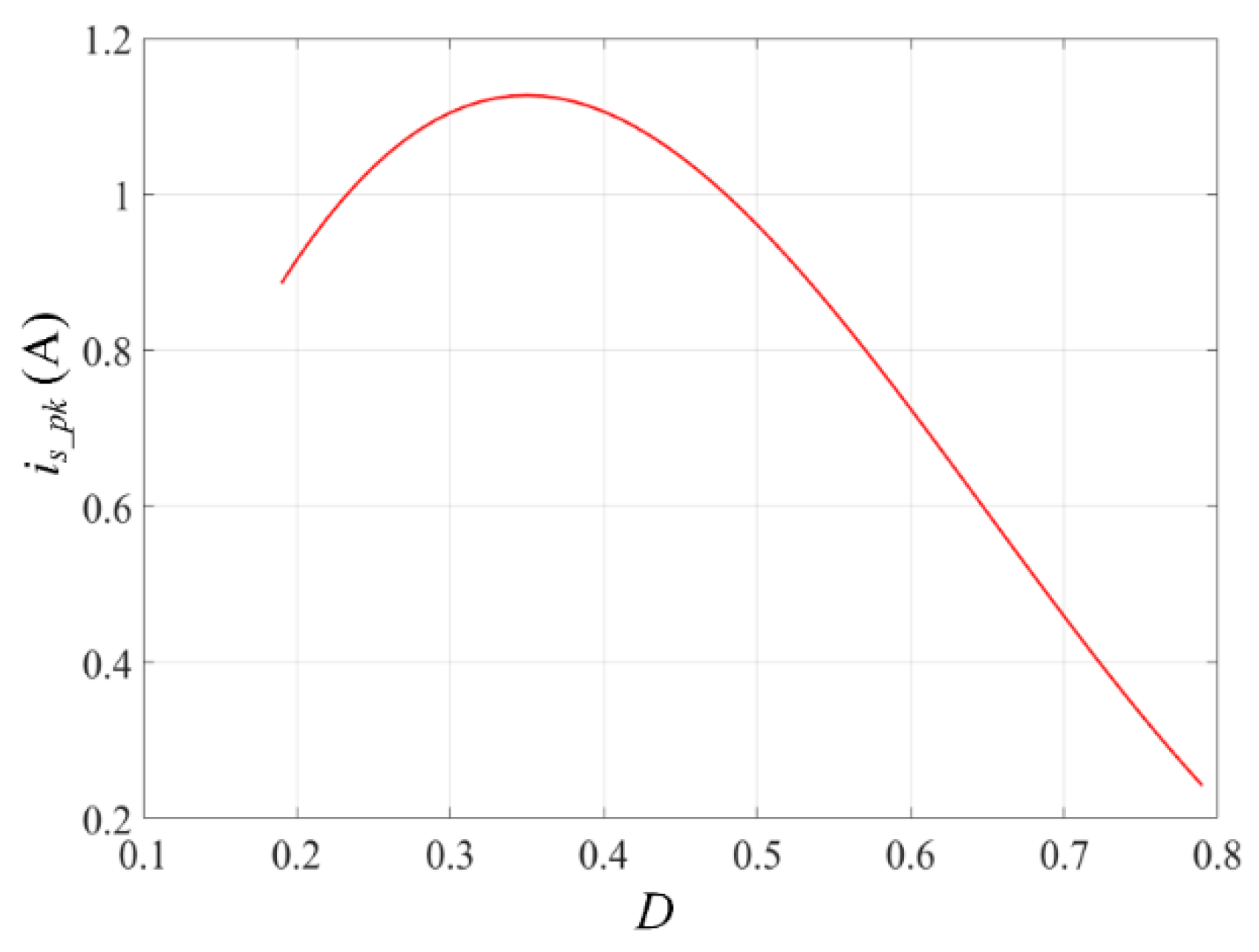
4.5. Peak Switch Current (is-pk)
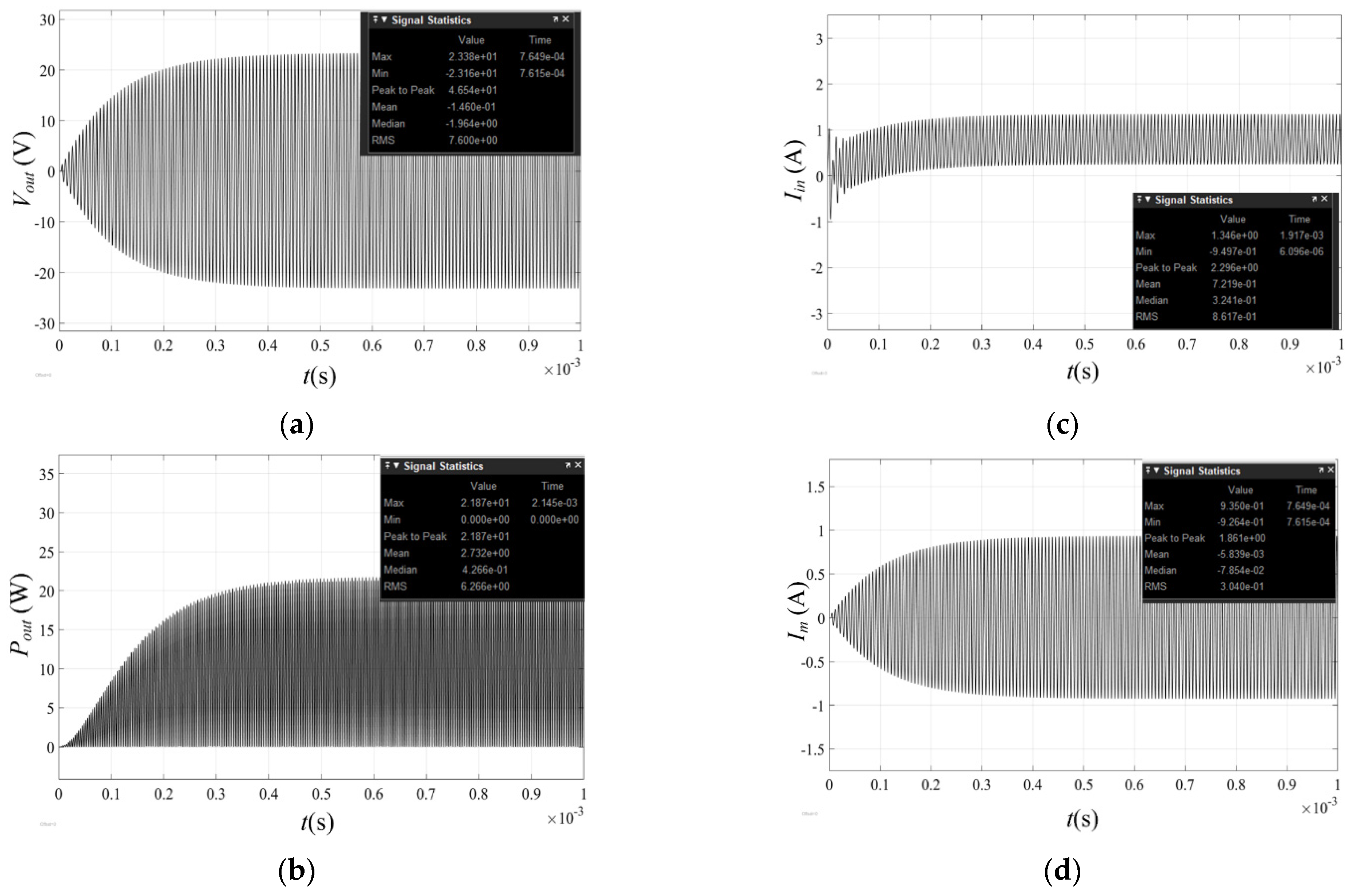
5. Simulation and Experimental Verification
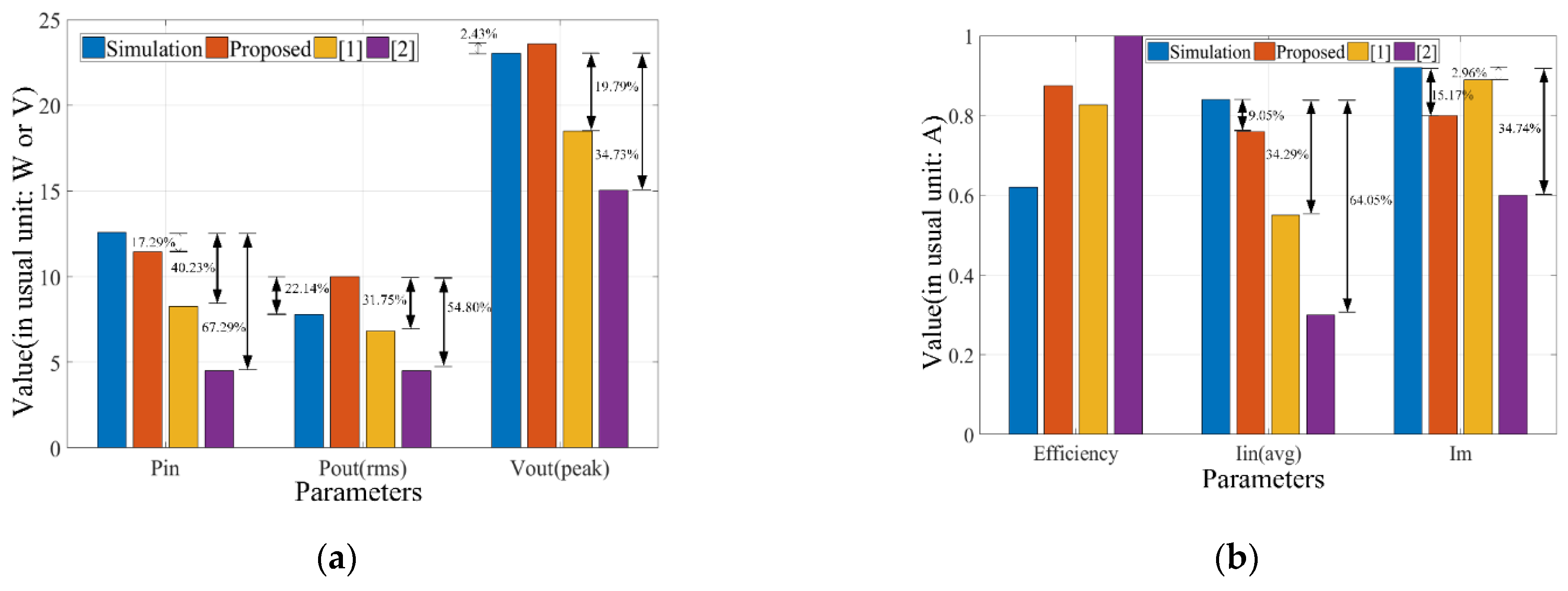
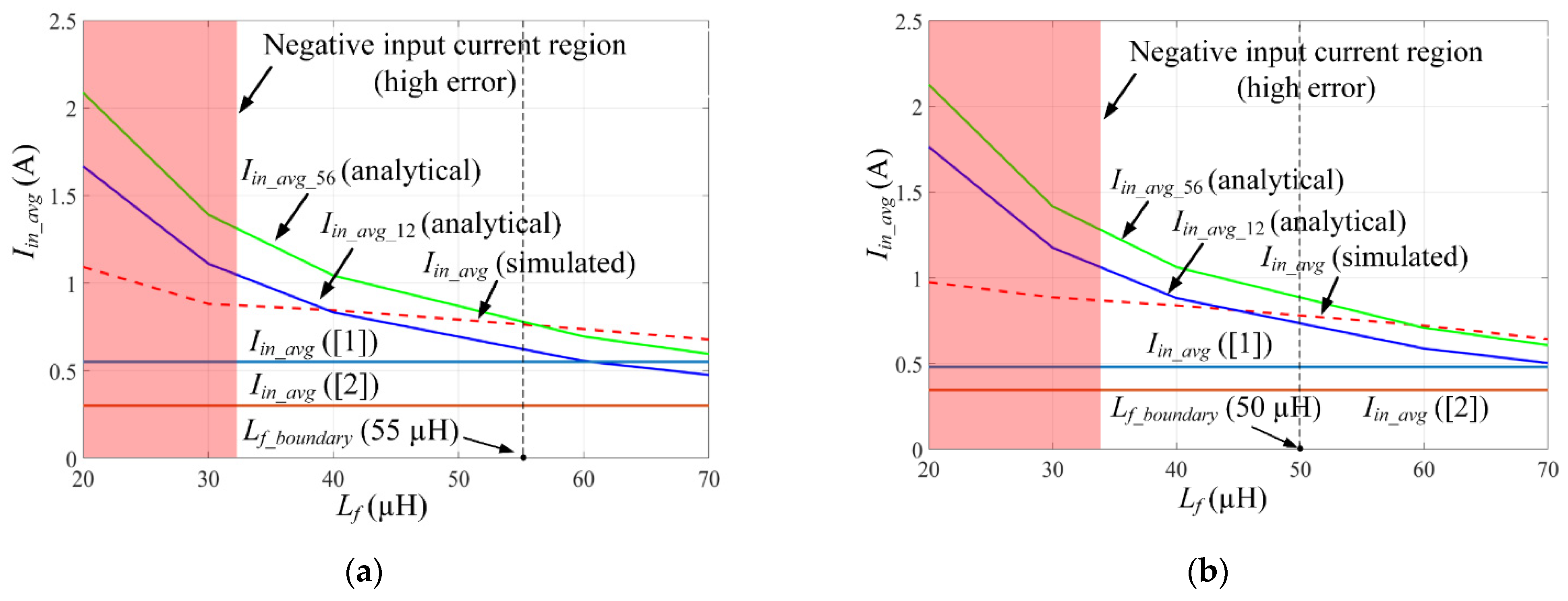
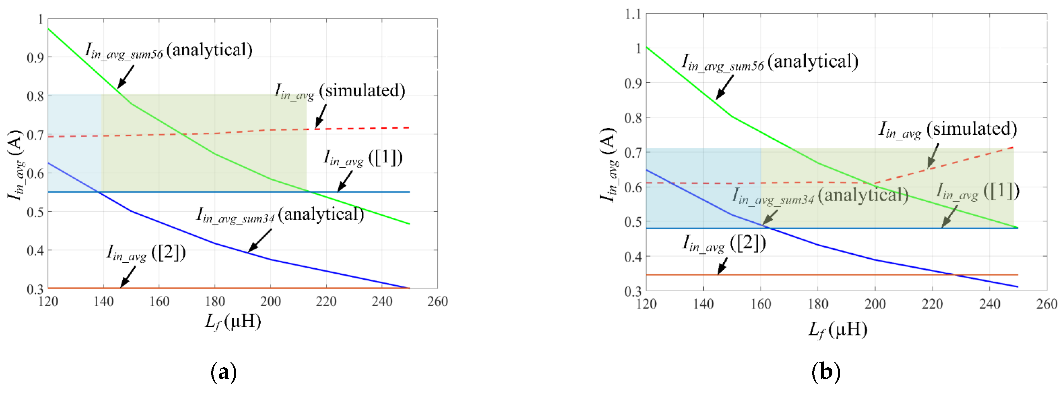
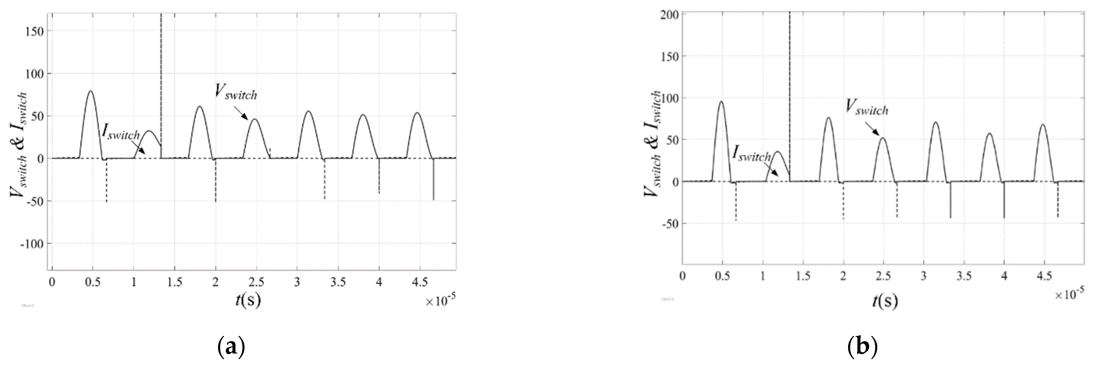
5.1. Case-2: The Continuous Conduction Mode (1 < N < 3)
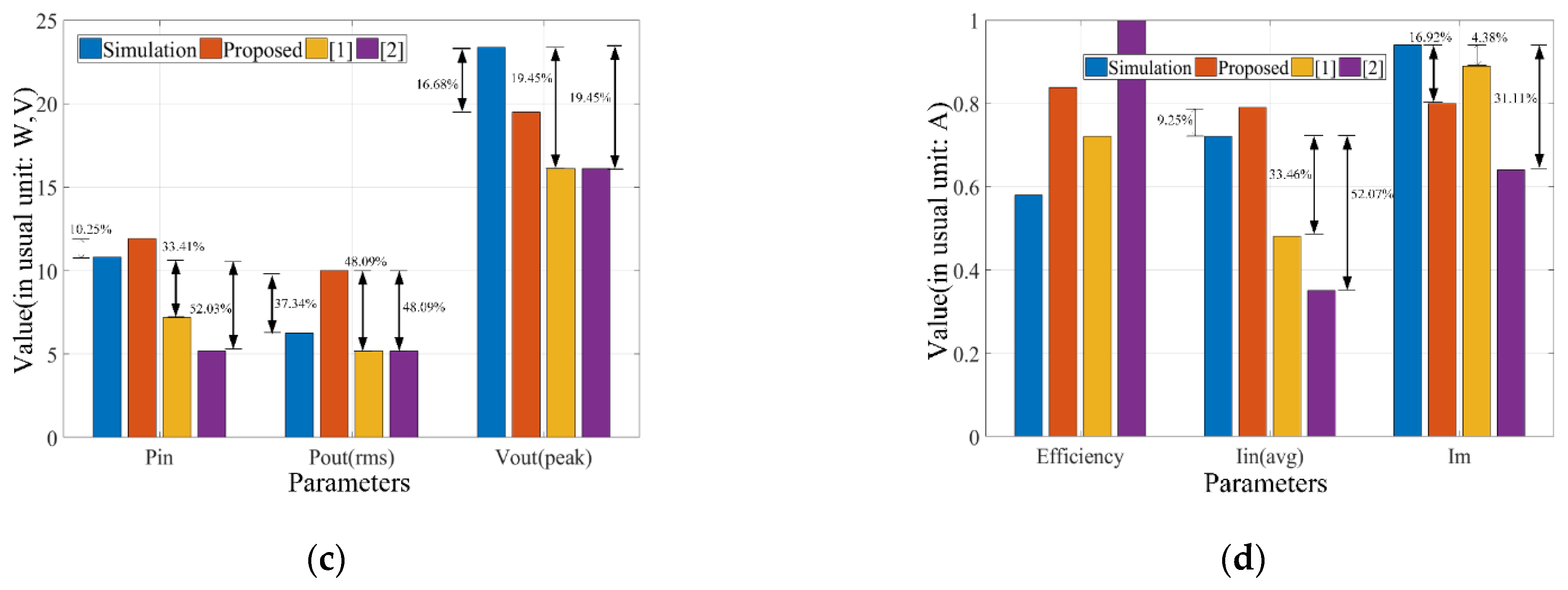
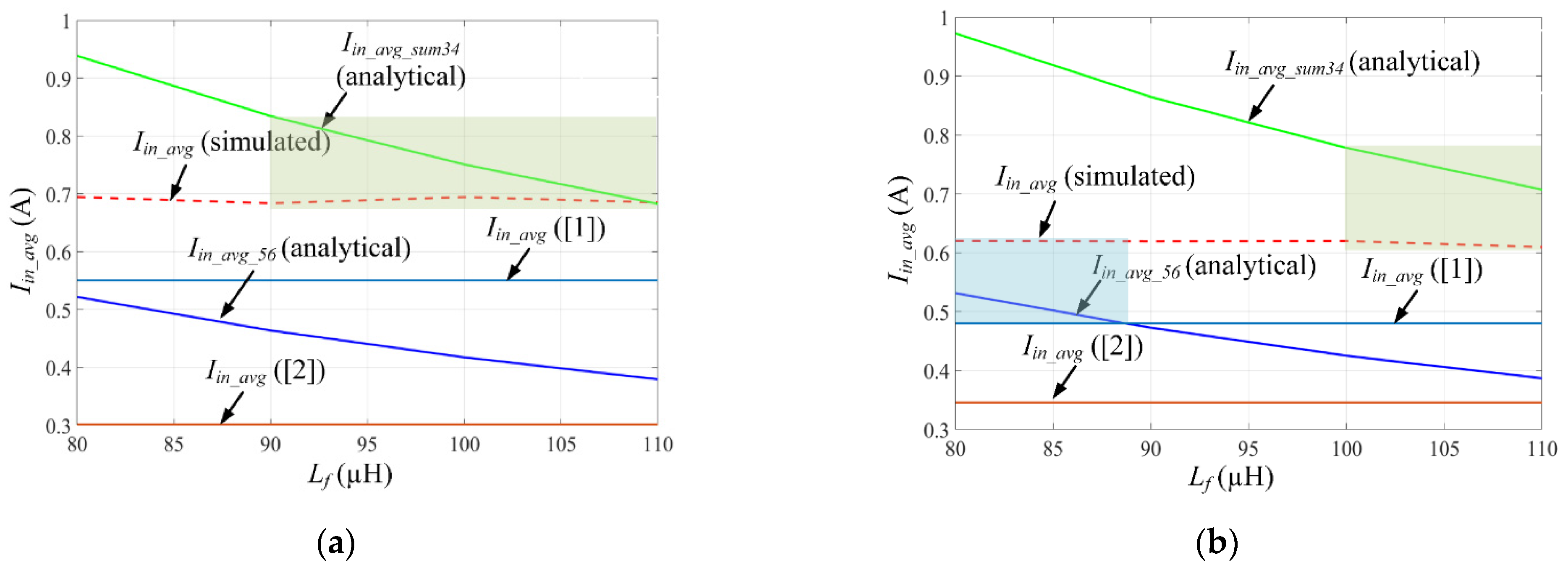
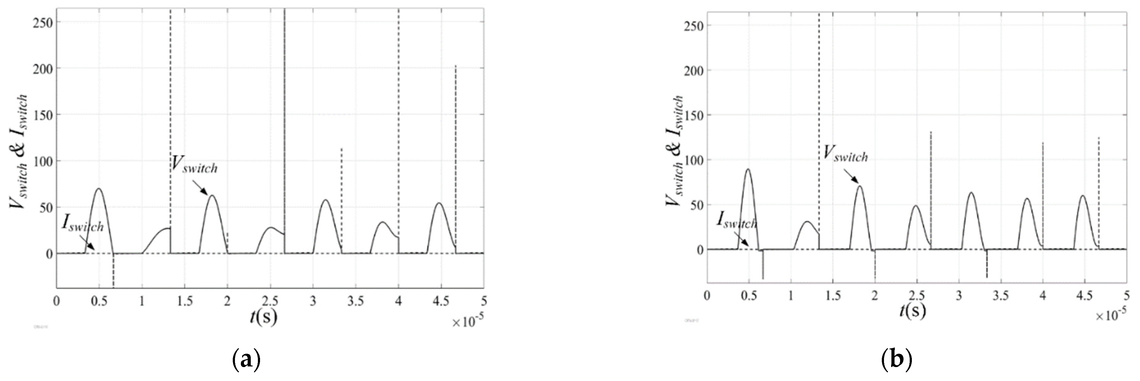
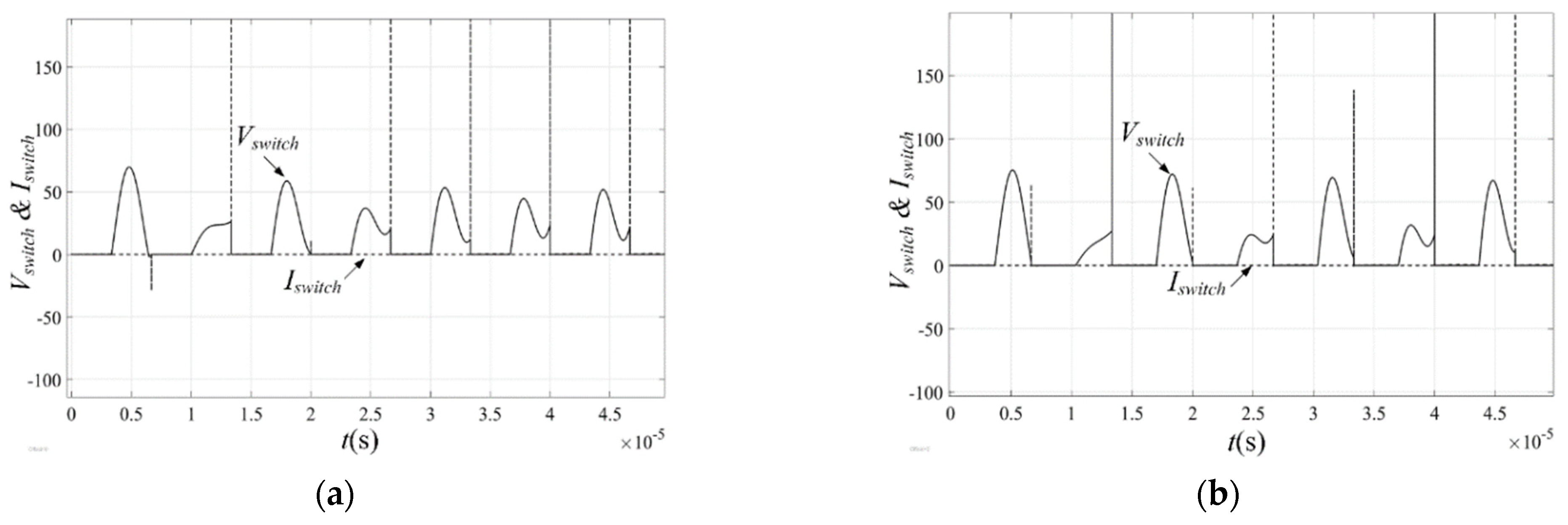
5.2. Case-3: The Continuous Conduction Mode (N > 3)
6. Conclusions
Author Contributions
Funding
Conflicts of Interest
Appendix A
References
- Hayati, M.; Lotfi, A.; Kazimierczuk, M.K.; Sekiya, H. Analysis and Design of Class-E Power Amplifier With MOSFET Parasitic Linear and Nonlinear Capacitances at Any Duty Ratio. IEEE Trans. Power Electron. 2013, 28, 5222–5232. [Google Scholar] [CrossRef]
- Ayachit, A.; Corti, F.; Reatti, A.; Kazimierczuk, M.K. Zero-Voltage Switching Operation of Transformer Class-E Inverter at Any Coupling Coefficient. IEEE Trans. Ind. Electron. 2019, 66, 1809–1819. [Google Scholar] [CrossRef]
- Hayati, M.; Roshani, S.; Roshani, S.; Kazimierczuk, M.K.; Sekiya, H. Design of Class E Power Amplifier with New Structure and Flat Top Switch Voltage Waveform. IEEE Trans. Power Electron. 2018, 33, 2571–2579. [Google Scholar] [CrossRef]
- Sheikhi, M.; Hayati, A.; Grebennikov, A. Design Methodology of Class-E/F3Power Amplifier Considering Linear External and Nonlinear Drain–Source Capacitance. IEEE Trans. Microw. Theory Tech. 2017, 65, 548–554. [Google Scholar] [CrossRef]
- Hayati, M.; Sheikhi, A.; Grebennikov, A. Design and Analysis of Class E/F3 Power Amplifier with Nonlinear Shunt Capacitance at Nonoptimum Operation. IEEE Trans. Power Electron. 2015, 30, 727–734. [Google Scholar] [CrossRef]
- Kessler, D.J.; Kazimierczuk, M.K. Power losses and efficiency of class-E power amplifier at any duty ratio. IEEE Trans. Circuits Syst. I Regul. Pap. 2004, 51, 1675–1689. [Google Scholar] [CrossRef]
- Thongsongyod, C.; Ekkaravarodome, C.; Jirasereeamornkul, K.; Boonyaroonate, I.; Higuchi, K. High step-up ratio DC-DC converter using Class-E resonant inverter and Class-DE rectifier for low voltage DC sources. In Proceedings of the 2016 International Conference on Electronics, Information, and Communications (ICEIC), Danang, Vietnam, 27–30 January 2016; pp. 1–4. [Google Scholar]
- Niyomthai, S.; Sangswang, A.; Naetiladdanon, S.; Mujjalinvimut, E. Operation region of class E resonant inverter for ultrasonic transducer. In Proceedings of the 2017 14th International Conference on Electrical Engineering/Electronics, Computer, Telecommunications and Information Technology (ECTI-CON), Phuket, Thailand, 27–30 June 2017; pp. 435–438. [Google Scholar]
- Rizo, L.; Ruiz, M.N.; García, J.A. Device characterization and modeling for the design of UHF Class-E inverters and synchronous rectifiers. In Proceedings of the 2014 IEEE 15th Workshop on Control and Modeling for Power Electronics (COMPEL), Santander, Spain, 22–25 June 2014; pp. 1–5. [Google Scholar]
- Ma, K.; Chang, W.; Lee, Y. A simple CLASS-E inverter design for driving ultrasonic welding system. In Proceedings of the 2009 International Conference on Power Electronics and Drive Systems (PEDS), Taipei, Taiwan, 2–5 November 2009; pp. 894–896. [Google Scholar]
- Ekbote, A.; Zinger, D.S. Comparison of Class E and Half Bridge Inverters for Use in Electronic Ballasts. In Proceedings of the Conference Record of the 2006 IEEE Industry Applications Conference Forty-First IAS Annual Meeting, Tampa, FL, USA, 8–12 October 2006; Volume 5, pp. 2198–2201. [Google Scholar]
- Ashique, R.H.; Khan, M.M.; Shihavuddin, A.; Maruf, M.H.; Al Mansur, A.; ul Haq, M.A. A Novel Family of Class EFnm and E/Fnm Inverter for Improved Efficiency. In Proceedings of the 2020 2nd International Conference on Sustainable Technologies for Industry 4.0 (STI), Dhaka, Bangladesh, 19–20 December 2020; pp. 1–6. [Google Scholar]
- Aldhaher, S.; Yates, D.C.; Mitcheson, P.D. Modeling and Analysis of Class EF and Class E/F Inverters with Series-Tuned Resonant Networks. IEEE Trans. Power Electron. 2016, 31, 3415–3430. [Google Scholar] [CrossRef] [Green Version]
- Kaczmarczyk, Z.; Jurczak, W.A. Push–Pull Class-E Inverter with Improved Efficiency. IEEE Trans. Ind. Electron. 2008, 55, 1871–1874. [Google Scholar] [CrossRef]
- Kazimierczuk, M.K.; Jozwik, J. DC/DC converter with class E zero-voltage-switching inverter and class E zero-current-switching rectifier. IEEE Trans. Circuits Syst. 1989, 36, 1485–1488. [Google Scholar] [CrossRef]
- Li, Y.; Sue, S. Exactly analysis of ZVS behavior for class E inverter with resonant components varying. In Proceedings of the 2011 6th IEEE Conference on Industrial Electronics and Applications, Beijing, China, 21–23 June 2011; pp. 1245–1250. [Google Scholar]


| Parameter | Value |
|---|---|
| Vin | 15 V |
| Vout_peak | 20 V |
| Pout_rms | 10 W |
| D | 0.50, 0.55 |
| fs, fr | 150 kHz |
| RL | 25 Ω |
| Cout | 10 nF |
| Cin | 13 nF and 72 nF |
| Lf | 50 µH and 55 µH |
| Lr | 1.3 mH |
| Cr | 865.99355 pF |
| D = 0.55 | ||||||
| Lf (µH) | Iin_avg_12 (Analytical) (A) | Iin_avg_56 (Analytical) (A) | Iin_avg (Simulation) (A) | Error percentage (Iin_avg_12 and simulation) (%) | Error percentage (Iin_avg_56 and simulation) (%) | Ripple (Simulation) (%) |
| 20 | 1.6671 | 2.0871 | 1.0930 | 52.53 | 90.95 | 365.96 |
| 30 | 1.1114 | 1.3914 | 0.8819 | 20.65 | 57.77 | 249.46 |
| 40 | 0.8335 | 1.0435 | 0.8462 | 1.50 | 23.31 | 189.08 |
| 60 | 0.5557 | 0.6957 | 0.7180 | 22.60 | 3.10 | 111.42 |
| 70 | 0.4763 | 0.5963 | 0.6787 | 29.82 | 12.14 | 221.01 |
| D = 0.50 | ||||||
| Lf (µH) | Iin_avg_12 (Analytical) (A) | Iin_avg_56 (Analytical) (A) | Iin_avg (Simulation) (A) | Error percentage (Iin_avg_12 and simulation) (%) | Error percentage (Iin_avg_56 and simulation) (%) | Ripple (Simulation) (%) |
| 20 | 1.7639 | 2.1261 | 0.9751 | 80.89 | 118.03 | 358.93 |
| 30 | 1.1759 | 1.4174 | 0.8859 | 32.73 | 59.99 | 237.04 |
| 40 | 0.8819 | 1.0630 | 0.8398 | 5.01 | 26.57 | 178.61 |
| 60 | 0.5880 | 0.7087 | 0.7219 | 18.54 | 1.82 | 145.44 |
| 70 | 0.5040 | 0.6075 | 0.6435 | 21.67 | 5.59 | 108.78 |
| D = 0.55 | ||||||
| Lf (µH) | Iin_avg_56 (Analytical) (A) | Iin_avg_sum34 (Analytical) (A) | Iin_avg (Simulation) (A) | Error percentage (Iin_avg_56 and simulation) (%) | Error percentage (Iin_avg_sum34 and simulation) (%) | Ripple (Simulation) (%) |
| 80 | 0.5218 | 0.9385 | 0.6945 | 24.86 | 35.13 | 115.19 |
| 90 | 0.4638 | 0.8343 | 0.6837 | 32.16 | 21.70 | 95.07 |
| 100 | 0.4174 | 0.7508 | 0.6944 | 39.89 | 8.12 | 86.40 |
| 110 | 0.3795 | 0.6826 | 0.6851 | 44.60 | 0.36 | 80.28 |
| D = 0.50 | ||||||
| Lf (µH) | Iin_avg_56 (Analytical) (A) | Iin_avg_sum34 (Analytical) (A) | Iin_avg (Simulation) (A) | Error percentage (Iin_avg_56 and simulation) (%) | Error percentage (Iin_avg_sum34 and simulation) (%) | Ripple (Simulation) (%) |
| 80 | 0.5315 | 0.9725 | 0.6200 | 14.27 | 56.85 | 129.17 |
| 90 | 0.4725 | 0.8644 | 0.6193 | 23.70 | 39.57 | 129.03 |
| 100 | 0.4252 | 0.7780 | 0.6198 | 31.39 | 25.52 | 80.67 |
| 110 | 0.3868 | 0.7072 | 0.6096 | 36.54 | 16.01 | 78.74 |
| D = 0.55 | ||||||
| Lf (µH) | Iin_avg_sum34 (Analytical) (A) | Iin_avg_sum56 (Analytical) (A) | Iin_avg (Simulation) (A) | Error percentage (Iin_avg_sum34 and simulation) (%) | Error percentage (Iin_avg_sum56 and simulation) (%) | Ripple (Simulation) (%) |
| 120 | 0.6257 | 0.9735 | 0.6936 | 9.78 | 40.35 | 72.08 |
| 150 | 0.5006 | 0.7788 | 0.6970 | 28.17 | 11.73 | 60.25 |
| 180 | 0.4171 | 0.6490 | 0.7021 | 40.59 | 7.56 | 54.12 |
| 200 | 0.3754 | 0.5841 | 0.7112 | 47.21 | 17.87 | 35.15 |
| 250 | 0.3003 | 0.4673 | 0.7169 | 58.11 | 34.81 | 27.89 |
| D = 0.50 | ||||||
| Lf (µH) | Iin_avg_sum34 (Analytical) (A) | Iin_avg_sum56 (Analytical) (A) | Iin_avg (Simulation) (A) | Error percentage (Iin_avg_sum34 and simulation) (%) | Error percentage (Iin_avg_sum56 and simulation) (%) | Ripple (Simulation) (%) |
| 120 | 0.6484 | 1.0027 | 0.6111 | 6.10 | 64.08 | 65.45 |
| 150 | 0.5187 | 0.8021 | 0.6095 | 14.89 | 31.59 | 49.22 |
| 180 | 0.4322 | 0.6684 | 0.6128 | 29.47 | 9.07 | 48.95 |
| 200 | 0.3890 | 0.6016 | 0.6101 | 36.23 | 1.39 | 42.61 |
| 250 | 0.3112 | 0.4813 | 0.7169 | 56.59 | 32.86 | 27.80 |
| Case | D | Lf (µH) | Cin (nF) | Pswitching_loss_rms (mW) | Percentage Loss (%) |
|---|---|---|---|---|---|
| 1 | 0.50 | 50 | 12 | 56.43 | 0.72 |
| 0.55 | 55 | 9 | 93.95 | 1.20 | |
| 0.60 | 70 | 5 | 150.8 | 1.93 | |
| 2 | 0.50 | 80 | 10 | 46.76 | 0.60 |
| 0.55 | 100 | 5 | 84.08 | 1.08 | |
| 0.60 | 80 | 5 | 118.7 | 1.52 | |
| 3 | 0.50 | 180 | 4 | 43.83 | 0.56 |
| 0.55 | 180 | 4 | 15.29 | 0.20 | |
| 0.60 | 200 | 2 | 99.33 | 1.27 |
Publisher’s Note: MDPI stays neutral with regard to jurisdictional claims in published maps and institutional affiliations. |
© 2021 by the authors. Licensee MDPI, Basel, Switzerland. This article is an open access article distributed under the terms and conditions of the Creative Commons Attribution (CC BY) license (https://creativecommons.org/licenses/by/4.0/).
Share and Cite
Ashique, R.H.; Shihavuddin, A.S.M.; Khan, M.M.; Islam, A.; Ahmed, J.; Arif, M.S.B.; Maruf, M.H.; Al Mansur, A.; Haq, M.A.u.; Siddiquee, A. An Analysis and Modeling of the Class-E Inverter for ZVS/ZVDS at Any Duty Ratio with High Input Ripple Current. Electronics 2021, 10, 1312. https://doi.org/10.3390/electronics10111312
Ashique RH, Shihavuddin ASM, Khan MM, Islam A, Ahmed J, Arif MSB, Maruf MH, Al Mansur A, Haq MAu, Siddiquee A. An Analysis and Modeling of the Class-E Inverter for ZVS/ZVDS at Any Duty Ratio with High Input Ripple Current. Electronics. 2021; 10(11):1312. https://doi.org/10.3390/electronics10111312
Chicago/Turabian StyleAshique, Ratil H., A. S. M. Shihavuddin, Mohammad Monirujjaman Khan, Aminul Islam, Jubaer Ahmed, M. Saad Bin Arif, Md Hasan Maruf, Ahmed Al Mansur, Mohammad Asif ul Haq, and Ashraf Siddiquee. 2021. "An Analysis and Modeling of the Class-E Inverter for ZVS/ZVDS at Any Duty Ratio with High Input Ripple Current" Electronics 10, no. 11: 1312. https://doi.org/10.3390/electronics10111312