
Analysis of a Resonant Converter with Wide Input Voltage


1
Department of Electrical Engineering, National Yunlin University of Science and Technology, Yunlin 640, Taiwan
2
College of Future, National Yunlin University of Science and Technology, Yunlin 640, Taiwan
*
Author to whom correspondence should be addressed.
Electronics 2021, 10(9), 1110; https://doi.org/10.3390/electronics10091110
Submission received: 24 April 2021
/
Revised: 2 May 2021
/
Accepted: 4 May 2021
/
Published: 8 May 2021
(This article belongs to the Section Power Electronics)
Abstract
:A DC-DC converter with a 16:1 (Vin,max = 16Vin,min) wide input voltage operation is presented for auxiliary power supplies on solar power conversion circuits or railway vehicles. The solar cell output voltage is associated with the solar intensity (day or night) and geographical location. Thus, the wide input voltage capability of DC converters is required for photovoltaic power conversion. For low power supplies on railway vehicles, the nominal input voltages are 24 V~110 V for the electric door system, motor drive, solid state lighting systems and braking systems. The presented converter uses buck/boost and resonant circuits to achieve the wide input voltage range operation from 18 V to 288 V. If Vin stays on a low input voltage range (18 V~72 V), the buck/boost circuit is operated at a voltage boost characteristic. On the other hand, the buck/boost circuit is operated at a voltage buck characteristic when the input voltage climbs to a high voltage range (72 V~288 V). Thus, the buck/boost circuit can output a constant voltage. Then, the resonant circuit in the second stage is worked at a constant input voltage case so that the frequency variation range is reduced. Finally, to investigate the performance and effectiveness of the studied circuit, experiments with a 500 W prototype were conducted to investigate the performance of the studied circuit.
1. Introduction
Wide voltage range DC-DC converters have been discussed and presented for solar cell power conversion due to the variable output voltage of the photovoltaic panel. The output voltage of a photovoltaic panel depends on the solar intensity of the day and night. Therefore, DC converters with a wide voltage range are developed for solar power conversion and the self-supplying power units are developed for remote control systems. Wide voltage DC-DC converters are also needed on a railway vehicle due to many different nominal DC voltages (24 V~110 V) that are requested for the communication system, lighting system, electric door system and braking system. Thus, pulse-width modulation (PWM) converters with a wide voltage operation are welcomed and demanded on railway power supply units. Multi-stage converters [1,2] have been proposed to actualize the wide voltage capability operation. The buck or boost circuit topology is selected on the front-stage to achieve a buck or boost operation. The flyback, forward or half-bridge circuit topology with pulse-width modulation is adopted on the rear-stage to regulate output voltage. However, these solutions have high switching losses on power devices and the input voltage range is still limited at Vin,max ≤ 4Vin,min or Vin,max ≤ 6Vin,min. Series-parallel connection DC converters have been discussed in [3,4,5]. Unfortunately, the circuit structure is too complicated and more expensive for use in low or medium power supplies. Single-stage DC converters with a PWM operation were discussed in [6,7,8,9,10,11,12] to extend the input voltage range. However, the input voltage range in [6,7,8,9,10,11,12] is still limited at Vin,max ≤ 4Vin,min. In [13], the thermal constraints issue has been discussed for a current-mode monolithic DC-DC converter.
In this paper, we present and investigate a DC-DC converter that has a 16:1 (Vin = 288 V~18 V) wide voltage operation and soft switching turn-on operation. To realize a 16:1 wide voltage operation, a buck/boost DC-DC circuit is utilized in the first stage to accomplish either a voltage boost action if the Vin is on a low input voltage range (Vin,min < Vin < 4Vin,min) or a voltage buck action if the Vin is on a high input voltage range (4Vin,min < Vin < 16Vin,min). Therefore, the output terminal voltage of the buck/boost converter is controlled at a constant value. An LLC converter is used in the rear-stage to control the output voltage while accomplishing zero voltage switching (ZVS) for active devices. Since the input voltage of the LLC converter is almost constant due to the buck/boost converter regulation, the variation in switching frequency is limited to a narrow frequency range. Compared to conventional DC-DC converters and multi-stage converters, the main contributions in this paper are (1) the wide voltage range action, (2) the soft switching operation in the second stage circuit, and (3) the simple control scheme. The converter characteristics are confirmed by the experiments using a prototype circuit.
2. Circuit Structure
Figure 1 provides the circuit schematic of the presented PWM converter with the function of a 16:1 voltage range operation for PV panel power converters or the auxiliary power on railway vehicles. The presented circuit is a two-stage DC converter. The front-stage is a buck/boost circuit and the rear-stage is an LLC converter. The components of a buck/boost circuit include Q1, D1, Lf, Q2, D2 and Cdc. The LLC converter includes Lr, S1, S2, T, Cr, Do1, Do2 and Co. The buck/boost circuit can achieve a wide input voltage range operation. When Vin < Vdc, the buck/boost circuit is operated at a voltage boost. On the other hand, the buck/boost circuit is worked at a buck operation if Vin > Vdc. The LLC resonant circuit in the rear-stage is operated at a constant input voltage Vdc condition. Therefore, the switching frequency of a resonant circuit can be designed at a series resonant frequency to lessen the magnetizing current losses, while, at the same time, having ZVS characteristics for switches S1 and S2 and diodes Do1 and Do2. According to the input voltage range, the presented converter can be operated at two voltage ranges (Vin,min~4Vin,min) and (4Vin,min~16Vin,min). When Vin is greater than Vin,min and less than 4Vin,min, the switch Q1 is on, diode D1 is on the reverse biased and Q2 is controlled with pulse-width modulation. Thus, the buck/boost circuit is worked like a boost converter to achieve a voltage step-up characteristic, as shown in Figure 2a. The DC bus voltage Vdc is controlled at the reference voltage Vdc,ref and the LLC resonant circuit is controlled at a constant input voltage case. When 4Vin,min < Vin < 16Vin,min, switch Q2 is off and switch Q1 is controlled with a pulse-width modulation scheme to control the DC bus voltage Vdc = Vdc,ref. Thus, the buck/boost converter is working as a buck converter to achieve a voltage step-down characteristic, as shown in Figure 2b. According to the adopted control algorithm, the studied converter has a 16:1 (Vin,max = 16Vin,min) voltage range operation for a solar PV panel power conversion and a railway vehicle with low power supplies and applications.
3. Operation Principle
The studied converter is a two-stage circuit. The front-stage is a buck/boost converter to achieve either a voltage boost action if Vin is on a low input voltage range or a voltage buck action if Vin is on a high input voltage range. The buck/boost converter is regulated by a pulse-width modulation. The second stage is an LLC resonant converter to accomplish both electric isolation and a ZVS turn-on operation for active devices.
3.1. Circuit Operation of the Buck/Boost Converter
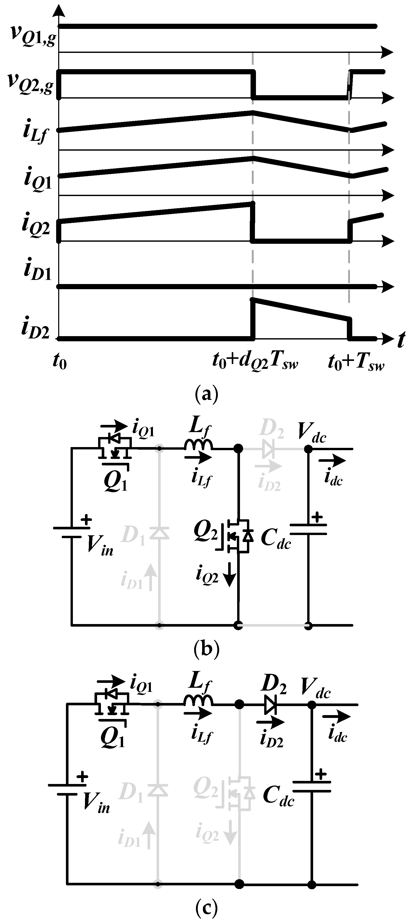
The buck/boost converter can work at a voltage boost operation or buck operation. To accomplish a wide voltage operation, the DC bus voltage of the buck/boost converter is controlled at Vdc = 4Vin,min. When Vin,min ≤ Vin < 4Vin,min, the buck/boost converter operates at a boost operation (Figure 2a)and Q1 is on, diode D1 is off and Q2 is controlled by a pulse-width modulation to have a voltage boost action. Figure 3a gives the PWM signals of the buck/boost converter for a voltage step-up action. Under a continuous conduction mode operation, two circuit modes are observed (Figure 3b,c). Based on a voltage-second balance on the inductor Lf, the DC bus voltage Vdc is obtained as dQ1Vin/(1 − dQ2) = Vin/(1 − dQ2) where dQ1 and dQ2 are duty cycles of Q1 and Q2, respectively, and dQ1 = 1 under the boost operation.
Mode 1 [t0~t0 + dQ2Tsw]: At t = t0, Q2 is activated to turn on. Since Q1 is always on and D1 is reverse biased for the voltage boost operation, the voltage across on Lf can be obtained as vLf = Vin and vD2 is −VDC. The inductor current iLf increases and the diode D2 is reverse biased. Capacitor Cdc is discharged to supply current idc to the secondstage resonant converter.
Mode 2 [t0 + dQ2Tsw~t0 + Tsw]: At t = t0 + dQ2Tsw, Q2 is turned off. The inductor iLf flows through D2 to charge Cdc. The inductor voltage vLf = Vin − Vdc < 0 so that iLf decreases. The drain-to-source voltage of Q2 is equal to the DC bus voltage Vdc. Mode 2 is ended at time t0 + Tsw.
When 4Vin,min < Vin ≤ 16Vin,min, the buck/boost converter operates as a voltage step-down operation (Figure 2b). The switch Q2 is controlled at an off state, diode D2 is always conducting and Q1 is activated by pulse-width modulation to accomplish a voltage step-down. The pulse-width modulation waveforms of the voltage step-down operation are given in Figure 4a and two circuit modes are shown in Figure 4b,c under a continuous conduction mode. Based on a flux balance on inductor Lf, the DC bus voltage Vdc is calculated as dQ1Vin/(1 − dQ2) = dQ1Vin where dQ2 = 0 under the buck operation.
Mode 1 [t0~t0 + dQ1Tsw]: At time t0, Q1 turns on. Since Q2 is always off and D2 is forward biased for the voltage step-down operation, the inductor voltage vLf = Vin − Vdc > 0 and vD1 is −Vin. In this mode, iLf increases, the D1 is reverse biased and Cdc is charged.
Mode 2 [t0 + dQ1Tsw~t0 + Tsw]: At time t0 + dQ1Tsw, Q1 turns off. In mode 2, vLf = −Vdc, iLf decreases, vQ1,ds = Vin, vQ2,ds = Vdc and Cdc is discharged. This mode ends at time t0 + Tsw.
3.2. Circuit Operation of the LLC Resonant Circuit
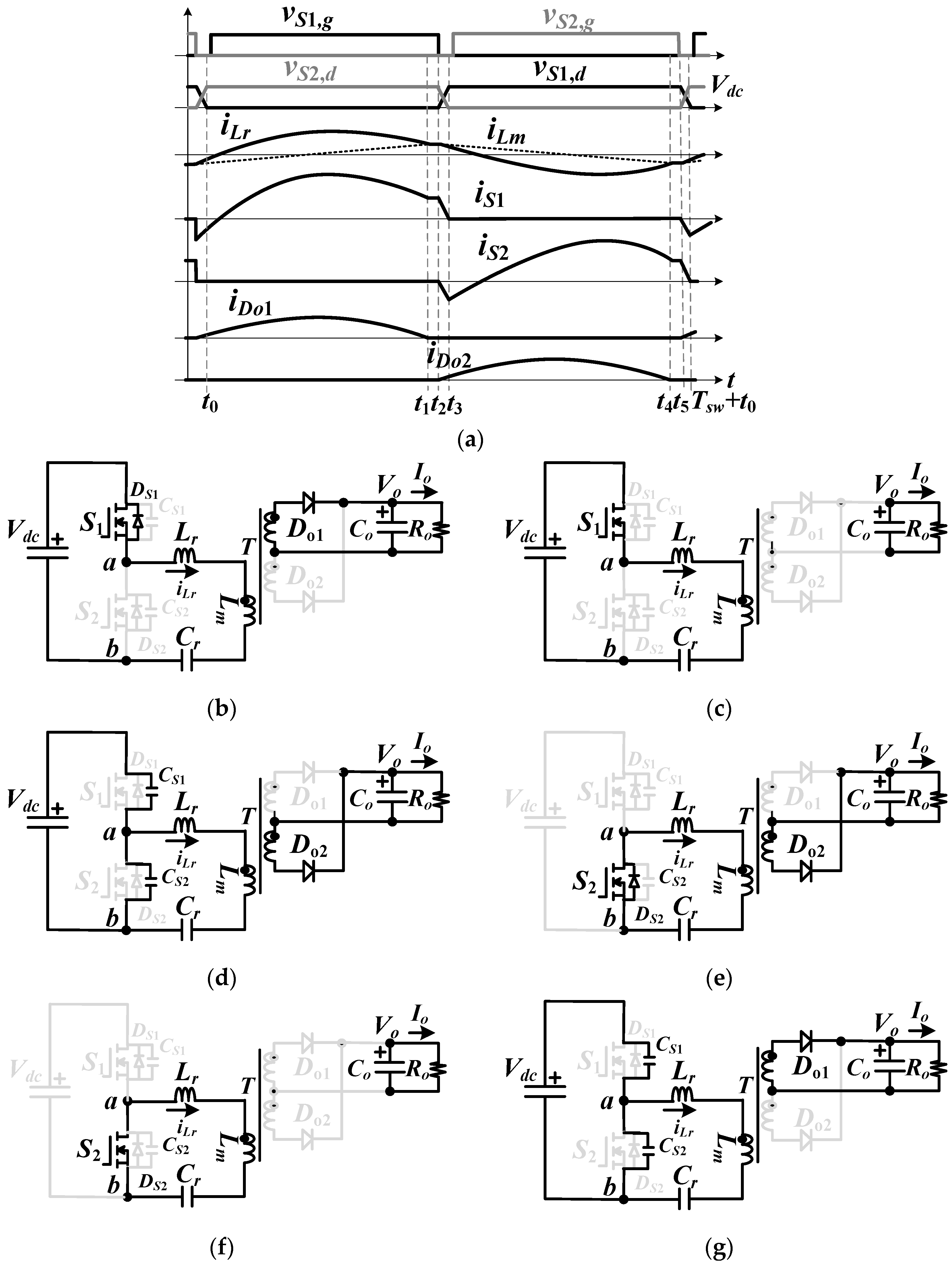
Since the DC bus voltage Vdc is a constant voltage due to the buck/boost circuit operation, the LLC resonant converter is operated under almost constant voltage Vdc. Thus, the switching frequency of the LLC resonant circuit is controlled at a limited narrow frequency range. The converter voltage gain is calculated as GLLC = 2nVo/Vdc = 2nVo (1 − dQ2)/dQ1Vin. Figure 5a gives the main circuit waveforms of the resonant converter and Figure 5b–g shows the six mode operations.
Mode 1 [t0~t1]: At time t < t0, the active device S1 is off, vCS1 is positive and iLr is negative. At time t0, vCS1 = 0 and DS1 is conducting. After time t0, S1 can turn on at the ZVS action. Since Do1 is conducting, vLm = nVo. Power is delivered to a load side through the components S1, Lr, T, Cr and Do1. Lr and Cr are naturally resonant, with frequency . If fr is greater than the switching frequency fsw, then the circuit proceeds to mode 2, or it goes to mode 3.
Mode 2 [t1~t2]: Since fr > fsw, iDo1 will decrease to 0 at t1. Do1 is off. iLr will flow through S1, Lm, Lr and Cr. Together with Lr and Lm, Cr is naturally resonant, with frequency and fm < fr.
Mode 3 [t2~t3]: Active device S1 is turned off at time t2 under zero voltage. After time t2, iLr > 0 and iLr < iLm. Thus, CS2 (CS1) discharges (charges) and the secondary diode Do2 conducts.
Mode 4 [t3~t4]: At time t3, CS2 is discharged to zero and DS2 is conducting due to iLr(t3) > 0. After t3, S2 turns on under zero voltage. Do2 is forward biased on the secondary side, vLm = −nVo. Energy stored on Cr is transferred to the output load. Lr and Cr are naturally resonant, with frequency fr.
Mode 5 [t4~t5]: If fsw < fr, then iD2 will decrease to 0 at t4. Do2 is reverse biased. No power is delivered to the output load. Lr, Lm and Cr are naturally resonant, with frequency fm.
Mode 6 [t5~Tsw + t0]: S2 turns off at time t5. CS1 (CS2) discharges (charges) and Do1 conducts because the iLr(t5) < 0 and iLr(t5) > iLm(t5). Mode 6 ends at time Tsw + t0.
4. Circuit Characteristics
The buck/boost converter is operated by a 16:1 wide voltage range operation. The output voltage Vdc of the buck/boost converter is controlled at Vdc,ref = 4Vin,min. If Vin is on a low voltage range (Vin < Vdc,ref = 4Vin,min), then the converter is operated at the boost operation. As a result, Q1 stays on, Q2 is operated by a duty cycle control and D1 is reverse biased. When Vin is on a high input voltage range (Vin > Vdc,ref = 4Vin,min), the converter is operated at a buck operation. As a result, Q2 stays off and Q1 is operated by pulse-width modulation. Thus, the LLC resonant circuit is operated at a constant input voltage of Vdc = 4Vin,min. The buck/boost converter is controlled at a continuous conduction mode. For the boost operation, VLf = Vin (or Vin − Vo) if Q2 is on (or off) as shown in Figure 3. For the buck operation, VLf = Vin − Vo (or −Vo) if Q1 is on (or off) as shown in Figure 4. For a continuous conduction mode, the DC bus voltage Vdc is calculated as:
where dQ1 and dQ2 are duty cycles of Q1 and Q2, respectively. Vin is greater than Vin,min and less than 4Vin,min on the low voltage range. Therefore, the maximum and minimum duty cycles of Q2 are expressed as:
In the same manner, the maximum and minimum duty cycles of Q1 are expressed as (4) and (5) on the high input voltage range (4Vin,min < Vin < 16Vin,min).
If the DC bus current and dQ1 and dQ2 are given, then the root mean square (rms) currents IQ1,rms and IQ2,rms are obtained in (6) and (7).
From the on/off states of Q1, Q2, D1 and D2, the voltage ratings of Q1 and Q2 are Vin,max and Vdc, respectively. The average currents ID1 and ID2 are obtained in (8) and (9).
Vin,max and Vdc are the voltage ratings of D1 and D2 respectively. Based on the boost or buck operation, the rms inductor current is calculated as:
The half-bridge resonant circuit is controlled with pulse frequency modulation. Since S1 and S2 have a 50% duty cycle, a square wave voltage waveform with 0 and Vdc is generated on voltage vab. The rms value of vab approximates . According to the conducting states of Do1 and Do2, a square voltage waveform is generated on the magnetizing voltage vLm and . The fundamental primary-side resistance is calculated as , where Ro is the DC load resistance. Since the resonant tank (Lm, Cr, Lr and Rac) is adopted in the rear-stage, in (11) the voltage transfer function of the resonant tank is obtained.
where LB = Lm/Lr, and fn = fsw/fr. Since the DC bus voltage Vdc is regulated at Vdc,ref by the front-stage buck/boost circuit, the switching frequency fsw depends on Io or Ro. The LLC resonant circuit is controlled at an inductive load. Therefore, active devices of the resonant circuit are operated using a soft switching operation.
5. Experimental Results
The studied circuit is tested and investigated to show the performance of the prototype circuit. The prototype is designed under the following specifications: Vin = 288 V~18 V (16:1 ratio), Vo = 12 V, Po,rated = 500 W and fr = 60 kHz. When Vin = 18 V~65 V, the buck/boost converter is controlled at boost operation. The voltage Vdc is maintained at 72 V. If the input voltage Vin = 76 V~288 V, then the buck/boost converter is operated at a buck operation and the DC bus voltage Vdc = 72 V. However, no voltage step-up or step-down is operated on the buck/boost converter when 65 V < Vin < 76 V. Q1 (Q2) is on (off) under this condition and Vdc = Vin. Therefore, the resonant circuit is designed under the input of a DC bus voltage Vdc = 65 V~76 V. Two Schmitt voltage comparators are used to detect the three input voltage ranges 18 V~65 V, 65 V~76 V and 76 V~288 V. If Vin is on a low voltage range (18 V~65 V), Q2 is controlled by a duty cycle scheme to achieve a boost operation. The duty cycle of Q2 is calculated in (12) and (13) under continuous conduction mode.
For a high input voltage range of 76 V~288 V, Q1 is controlled by a duty cycle scheme to achieve a buck operation. The duty cycle of Q1 is given in (14) and (15) under continuous conduction mode.
It is assumed that the ripple current ΔiLf is 5% of the maximum input current at 18 V of input voltage. Therefore, inductance Lf is given in (16).
The rms switch currents IQ1,rms and the IQ2,rms are expressed in (17) and (18).
The voltage ratings of Q1 and Q2 are Vin,max = 288 V and Vdc,max = 76 V. Switch Q1 used two MOSFETs STB35N60DM2 (STMicroelectronics, Geneva, Switzerland) with 600 V/28 A ratings, while switch Q2 adopted MOSFET IRFB4110PbF (Infineon Technologies, Neubiberg, Germany) with 100 V/120 A ratings. The average diode currents of D1 and D2 are obtained in (19) and (20).
D1 has a voltage stress of Vin,max = 288 V and D2 has a voltage stress of Vdc,max = 76 V. SF1006G (TSMC, Hsinchu, Taiwan) and STPS20SM100S (STMicroelectronics, Geneva, Switzerland) with 400 V/10 A and 100 V/20 A ratings are used for diodes D1 and D2, respectively.
For the LLC resonant circuit design, the necessary resonant frequency and inductor ratio are selected as fr = 60 kHz and LB = 8. The minimum, nominal and maximum DC bus voltages are 65 V, 72 V and 76 V, respectively. The nominal voltage gain of Gnom at Vdc,nom = 72 V is designed at unity. Therefore, the turn-ratio n of the transformer is calculated as follows.
The TDK EER42 with ns = 4 and np = 12 is used for the transformer T. Thus, the voltage gains GLLC,max and GLLC,min at Vdc = 65 V and 76 V are calculated in (22) and (23).
For full rated power, the fundamental primary-side resistance Rac is obtained in (24).
The selected quality factor Q is 0.7. From the given Q, Rac and fr, the resonant inductance Lr is obtained as:
due to LB = 8, Lm = LB × Lr = 31.2 μH. Cr can be calculated as:
The voltage ratings of S1 and S2 equal Vdc,max = 76 V and the voltage rating of diodes Do1 and Do2 equals 2Vo = 24 V. Power switches IPP111N15N3 (150 V/83 A) are adopted for active devices S1 and S2 and S60SC6M (60 V/60 A) (Shindengen Electric Manufacturing, Tokyo, Japan) switches are selected for Do1 and Do2. The selected Cdc = 680 μF and Co = 1000 μF. UC3843 (Texas Instruments, Dallas, TX, USA) is selected to regulate the buck/boost circuit while the UCC25600 (Texas Instruments, Dallas, TX, USA) is adopted to regulate the LLC resonant circuit.
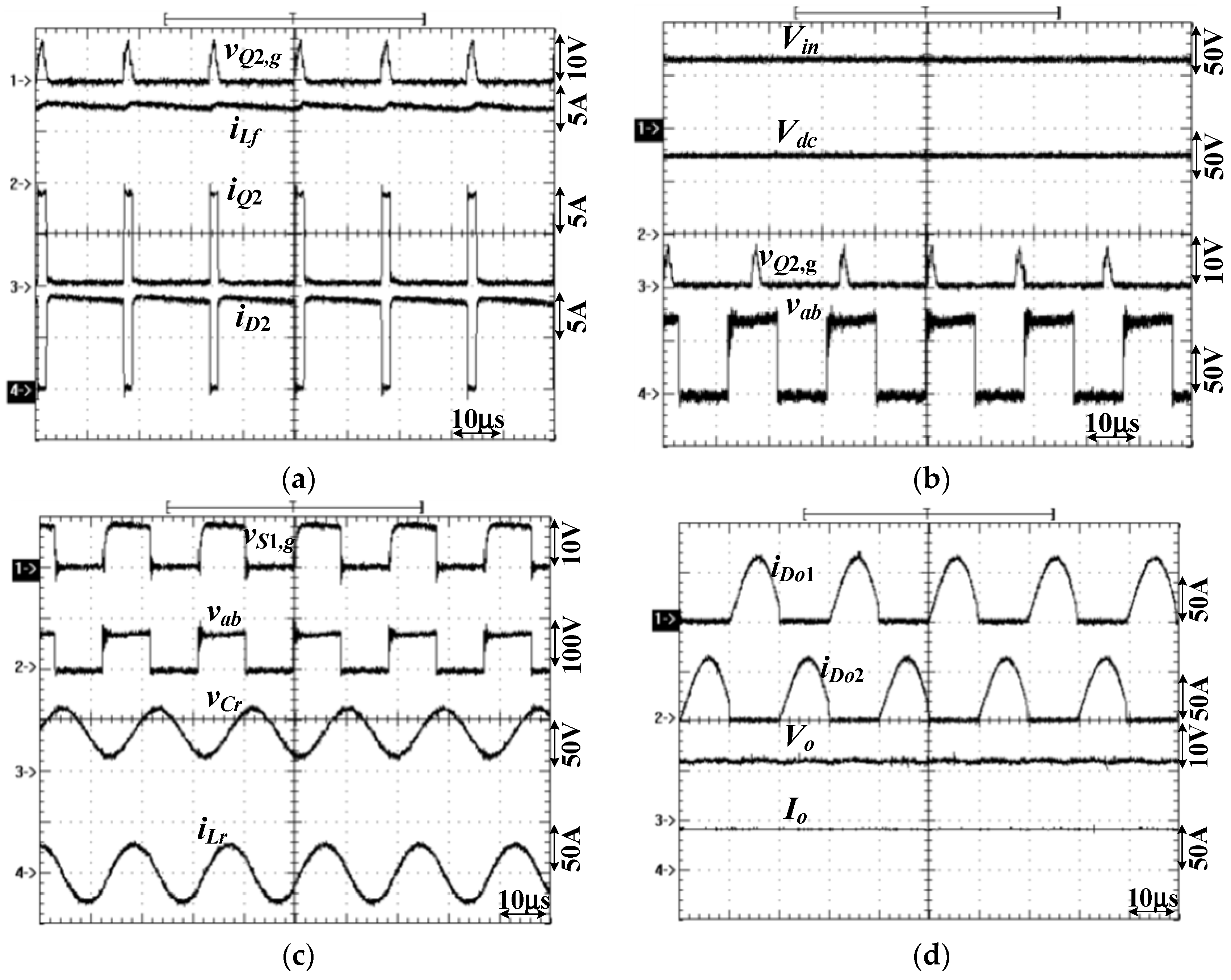
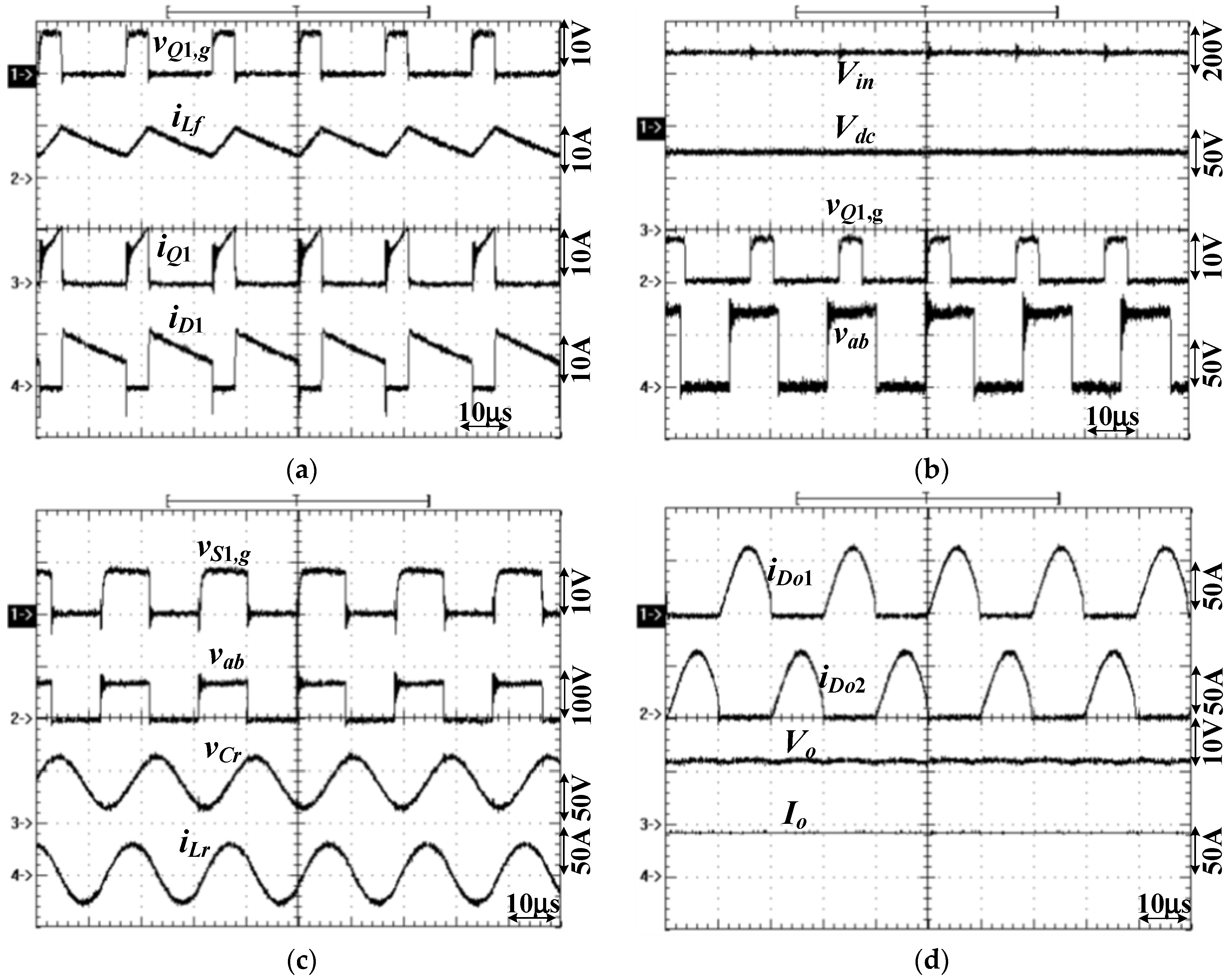
Figure 6 illustrates the experiments of the presented converter at Vin = 18 V and the rated power. Since Vin = 18 V < Vdc = 72 V, the buck/boost converter is operated at a boost operation. Therefore, Q1 is on and Q2 is controlled by the duty cycle modulation. Figure 6a shows the experimental waveforms of vQ2,g, iLf, iQ2 and iD2. When Q2 is on or off, the iLf equals iQ2 or iD2. Figure 6b provides the test results of the input voltage Vin, dc bus voltage Vdc, the gate voltage vQ2,g and leg voltage vab. The duty cycle of Q2 equals 0.75, Vdc > Vin (boost operation) and the leg voltage vab is a square voltage. Figure 6c gives the primary-side experimental waveforms of the LLC resonant circuit at full load. As the switching frequency is close to the resonant frequency, vCr and iLr are sinusoidal waveforms and vab is a square waveform. Since the half-bridge LLC is controlled in the second stage, the vCr contains a DC voltage value (vCr,dc = Vdc/2). Figure 6d provides the secondary side currents and load voltage at full load. The output voltage is regulated at 12 V and the load current Io = 42 A. No serious reverse recovery current is observed on the rectifier diodes Do1 and Do2. In the same manner, Figure 7 illustrates the experiments at Vin = 65 V and the rated power conditions. Since Vin = 65 V < Vdc = 72 V, the duty cycle of Q2 is calculated as 0.1. The measured waveforms vQ2,g, iLf, iQ2 and iD2 are shown in Figure 7a. The experimental waveforms Vin, Vdc, vQ2,g and vab are illustrated in Figure 7b. The experimental waveforms of the resonant converter are provided in Figure 7c,d. Since Vdc = 72 V by the buck/boost converter for both Vin = 18 V and 65 V, it can be seen that the measured waveforms of the resonant converter under Vin = 18 V (Figure 6c,d) and Vin = 65 V (Figure 7c,d) are identical. Figure 8 and Figure 9 show the experiments of the proposed circuit for Vin = 76 V and 288 V input on the high input voltage range and rated power. When the input voltage ranges between 76 V and 288 V, the buck/boost circuit is controlled at a buck operation and Q2 is off. The duty cycle of Q1 equals 0.95 (0.25) at Vin = 76 V (288 V). The measured waveforms of vQ1,g, iLf, iQ1 and iD1 at Vin = 76 V and 288 V are illustrated in Figure 8a and Figure 9a. The buck/boost converter is operated at a buck operation and Vdc is controlled at 72 V for both Vin = 76 V and Vin = 288 V. The experiments of the resonant converter for a 76 V (288 V) input are shown in Figure 8c,d (Figure 9c,d). When 65 V < Vin < 76 V, Q1 is on and Q2 is off. No voltage step-up or step-down is realized on the buck/boost converter so that the DC bus voltage Vdc = Vin. Under this condition, only the resonant converter is worked to regulate the load voltage. Figure 10 and Figure 11 provide the measured waveforms of the resonant circuit at 67 V and 74 V input and the rated power. When Vdc = 67 V, the resonant converter needs more voltage gain compared to Vdc = 72 V and fsw < fr. Thus, iLr likes a quasi-sinusoidal signal in Figure 10a and Do1 and Do2 are turned off at zero current switching in Figure 10b. In the same manner, the switching frequency at Vdc = 74 V shown in Figure 11 is greater than the resonant frequency in order to achieve a lower voltage gain. Figure 12 illustrates the experiments of S1 at Vin = 18 V, 67 V, 74 V and 288 V. Figure 12a,b shows the experimental waveforms of S1 under 20% load and full load at Vin = 18 V condition. In the same manner, Figure 12c,d gives the measured results of S1 at 67 V input. Figure 12e,f provides the test results of S1 at 74 V input. Likewise, Figure 12g,h shows the experimental waveforms of S1 at 288 V input (high input voltage range). From the test results in Figure 12, it can be seen that S1 turns on at ZVS from a 20% load for all input voltage ranges and turns off at hard switching. Since switch S2 possesses the same switching characteristics as S1, it can be expected that S2 also turns on under zero voltage from a 20% load and turns off at hard switching.
6. Conclusions
A wide input voltage (18 V~288 V) DC converter is discussed and examined for railway vehicles or for PV power conversion. To realize a 16:1 wide input voltage demand, a buck/boost circuit is used to accomplish the boost operation if Vin is on a low input voltage range and a buck operation if Vin is on a high input voltage range. Therefore, the DC bus voltage after the buck/boost converter is kept at a constant voltage. The resonant converter is employed on the rear-stage to achieve electric isolation and have a soft switching operation for active switches and power diodes. Since the LLC resonant converter is operated at a constant input voltage, the switching frequency variation is limited at a narrow frequency range. The performance of the studied circuit is investigated and examined through the test results.
Author Contributions
Writing—original draft, investigation, methodology, conceptualization, visualization, B.-R.L.; writing—review and editing, A.P.I.G.; validation, K.-W.W. All authors have read and agreed to the published version of the manuscript.
Funding
This research is supported by the Ministry of Science and Technology (MOST), Taiwan, under grant number MOST 108-2221-E-224-022-MY2.
Conflicts of Interest
The authors declare no conflict of interest.
References
- Shang, C.; Liu, L.; Liu, M.; Men, S. A highly-efficient two-stage DC-DC converter with wide input voltage. In Proceedings of the 2015 IEEE International Telecommunications Energy Conference, Osaka, Japan, 18–22 October 2015; pp. 1–6. [Google Scholar]
- Jeong, Y.; Kim, J.K.; Lee, J.B.; Moon, G.W. An asymmetric half-bridge resonant converter having a reduced conduction loss for DC/DC power applications with a wide range of low input voltage. IEEE Trans. Power Electron. 2017, 32, 7795–7804. [Google Scholar] [CrossRef]
- Wang, P.; Zhou, L.; Zhang, Y.; Li, J.; Sumner, M. Input-parallel output-series DC-DC boost converter with a wide input voltage range, for fuel cell vehicles. IEEE Trans. Veh. Technol. 2017, 66, 7771–7781. [Google Scholar] [CrossRef]
- Zhang, Y.; Fu, C.; Sumner, M.; Wang, P. A wide input-voltage range quasi-Z-source boost DC–DC converter with high-voltage gain for fuel cell vehicles. IEEE Trans. Ind. Electron. 2018, 65, 5201–5212. [Google Scholar] [CrossRef] [Green Version]
- Yao, Z.; Xu, J. A three-phase DC-DC converter for low and wide input-voltage range application. In Proceedings of the 2016 IEEE Transportation Electrification Conference and Expo, Busan, Korea, 1–4 June 2016; pp. 208–213. [Google Scholar]
- Li, W.; Zong, S.; Liu, F.; Yang, H.; He, X.; Wu, B. Secondary-side phase-shift-controlled ZVS DC/DC converter with wide voltage gain for high input voltage applications. IEEE Trans. Power Electron. 2013, 28, 5128–5139. [Google Scholar] [CrossRef]
- Lin, B.R. Zero-voltage dc/dc converter with asymmetric pulse-width modulation for dc micro-grid system. Int. J. Electron. 2018, 105, 679–693. [Google Scholar] [CrossRef]
- Lu, J.; Kumar, A.; Afridi, K.K. Step-down impedance control network resonant DC-DC converter utilizing an enhanced phase-shift control for wide-input-range operation. IEEE Trans. Ind. Appl. 2018, 54, 4523–4536. [Google Scholar] [CrossRef]
- Wang, X.; Tian, F.; Batarseh, I. High efficiency parallel post regulator for wide range input DC–DC converter. IEEE Trans. Power Electron. 2008, 23, 852–858. [Google Scholar] [CrossRef]
- Lin, B.R. Series resonant converter with auxiliary winding turns: Analysis, design and implementation. Int. J. Electron. 2018, 105, 836–847. [Google Scholar] [CrossRef]
- Wu, H.; Wan, C.; Sun, K.; Xing, Y. A high step-down multiple output converter with wide input voltage range based on quasi two-stage architecture and dual-output LLC resonant converter. IEEE Trans. Power Electron. 2015, 30, 1793–1796. [Google Scholar] [CrossRef]
- Lin, B.R. Novel ZVS DC-DC converter with low current ripple for light rail transit. Int. J. Electron. 2019, 106, 567–580. [Google Scholar] [CrossRef]
- Xiao, Z.; Wang, Y.; Zhao, G.; Xu, Y.; Lu, C.; Hu, W. A power-switch thermal limiting technique for current-mode monolithic DC-DC converters. Int. J. Electron. Commun. 2019, 111, 152797. [Google Scholar] [CrossRef]
Figure 1.
The circuit diagram of the presented converter with 16:1 (Vin,max = 16Vin,min) voltage range operation.
Figure 1.
The circuit diagram of the presented converter with 16:1 (Vin,max = 16Vin,min) voltage range operation.

Figure 2.
Equivalent circuits for (a) low input voltage operation (b) high input voltage operation.

Figure 3.
Buck/boost converter under low voltage range (boost operation) (a) pulse-width modulation (PWM) signals (b) mode 1 equivalent circuit (c) mode 2 equivalent circuit.
Figure 3.
Buck/boost converter under low voltage range (boost operation) (a) pulse-width modulation (PWM) signals (b) mode 1 equivalent circuit (c) mode 2 equivalent circuit.

Figure 4.
Buck/boost converter under high voltage range (buck operation) (a) PWM signals (b) mode 1 equivalent circuit (c) mode 2 equivalent circuit.
Figure 4.
Buck/boost converter under high voltage range (buck operation) (a) PWM signals (b) mode 1 equivalent circuit (c) mode 2 equivalent circuit.

Figure 5.
Circuit operations of resonant converter (a) PWM signals (b) mode 1 equivalent circuit (c) mode 2 equivalent circuit (d) mode 3 equivalent circuit (e) mode 4 equivalent circuit (f) mode 5 equivalent circuit (g) mode 6 equivalent circuit.
Figure 5.
Circuit operations of resonant converter (a) PWM signals (b) mode 1 equivalent circuit (c) mode 2 equivalent circuit (d) mode 3 equivalent circuit (e) mode 4 equivalent circuit (f) mode 5 equivalent circuit (g) mode 6 equivalent circuit.

Figure 6.
Measured results at Vin = 18 V and Po = 500 W (a) vQ2,g, iLf, iQ2 and iD2 (b) Vin, Vdc, vQ2,g and vab (c) vS1,g, vab, vCr and iLr (d) iDo1, iDo2, Vo and Io.
Figure 6.
Measured results at Vin = 18 V and Po = 500 W (a) vQ2,g, iLf, iQ2 and iD2 (b) Vin, Vdc, vQ2,g and vab (c) vS1,g, vab, vCr and iLr (d) iDo1, iDo2, Vo and Io.

Figure 7.
Measured results at Vin = 65 V and Po = 500 W (a) vQ2,g, iLf, iQ2 and iD2 (b) Vin, Vdc, vQ2,g and vab (c) vS1,g, vab, vCr and iLr (d) iDo1, iDo2, Vo and Io.
Figure 7.
Measured results at Vin = 65 V and Po = 500 W (a) vQ2,g, iLf, iQ2 and iD2 (b) Vin, Vdc, vQ2,g and vab (c) vS1,g, vab, vCr and iLr (d) iDo1, iDo2, Vo and Io.

Figure 8.
Measured results at Vin = 76 V and Po = 500 W (a) vQ1,g, iLf, iQ1 and iD1 (b) Vin, Vdc, vQ1,g and vab (c) vS1,g, vab, vCr and iLr (d) iDo1, iDo2, Vo and Io.
Figure 8.
Measured results at Vin = 76 V and Po = 500 W (a) vQ1,g, iLf, iQ1 and iD1 (b) Vin, Vdc, vQ1,g and vab (c) vS1,g, vab, vCr and iLr (d) iDo1, iDo2, Vo and Io.

Figure 9.
Measured results at Vin = 288 V and Po = 500 W (a) vQ1,g, iLf, iQ1 and iD1 (b) Vin, Vdc, vQ1,g and vab (c) vS1,g, vab, vCr and iLr (d) iDo1, iDo2, Vo and Io.
Figure 9.
Measured results at Vin = 288 V and Po = 500 W (a) vQ1,g, iLf, iQ1 and iD1 (b) Vin, Vdc, vQ1,g and vab (c) vS1,g, vab, vCr and iLr (d) iDo1, iDo2, Vo and Io.

Figure 10.
Measured results at Vin = 67 V and Po = 500 W (a) vS1,g, vab, vCr and iLr (b) iDo1, iDo2, Vo and Io.
Figure 10.
Measured results at Vin = 67 V and Po = 500 W (a) vS1,g, vab, vCr and iLr (b) iDo1, iDo2, Vo and Io.

Figure 11.
Measured results at Vin = 74 V and Po = 500 W (a) vS1,g, vab, vCr and iLr (b) iDo1, iDo2, Vo and Io.
Figure 11.
Measured results at Vin = 74 V and Po = 500 W (a) vS1,g, vab, vCr and iLr (b) iDo1, iDo2, Vo and Io.

Figure 12.
Experiments of switch S1 of resonant converter at (a) Vin = 18 V and 20% power (b) Vin = 18 V and full power (c) Vin = 67 V and 20% power (d) Vin = 67 V and full power (e) Vin = 74 V and 20% power (f) Vin = 74 V and full power (g) Vin = 288 V and 20% power (h) Vin = 288 V and full power.
Figure 12.
Experiments of switch S1 of resonant converter at (a) Vin = 18 V and 20% power (b) Vin = 18 V and full power (c) Vin = 67 V and 20% power (d) Vin = 67 V and full power (e) Vin = 74 V and 20% power (f) Vin = 74 V and full power (g) Vin = 288 V and 20% power (h) Vin = 288 V and full power.

Publisher’s Note: MDPI stays neutral with regard to jurisdictional claims in published maps and institutional affiliations. |
© 2021 by the authors. Licensee MDPI, Basel, Switzerland. This article is an open access article distributed under the terms and conditions of the Creative Commons Attribution (CC BY) license (https://creativecommons.org/licenses/by/4.0/).
Share and Cite
MDPI and ACS Style
Lin, B.-R.; Goh, A.P.I.; Wang, K.-W. Analysis of a Resonant Converter with Wide Input Voltage. Electronics 2021, 10, 1110. https://doi.org/10.3390/electronics10091110
AMA Style
Lin B-R, Goh API, Wang K-W. Analysis of a Resonant Converter with Wide Input Voltage. Electronics. 2021; 10(9):1110. https://doi.org/10.3390/electronics10091110
Chicago/Turabian StyleLin, Bor-Ren, Alexis Phaik Imm Goh, and Kai-Wei Wang. 2021. "Analysis of a Resonant Converter with Wide Input Voltage" Electronics 10, no. 9: 1110. https://doi.org/10.3390/electronics10091110
Note that from the first issue of 2016, this journal uses article numbers instead of page numbers. See further details here.