
Modulated High Power and Narrow Pulse Width Laser Drive Circuit for Lidar System

School of Information Science and Technology, Fudan University, Shanghai 200433, China
*
Authors to whom correspondence should be addressed.
Electronics 2021, 10(7), 823; https://doi.org/10.3390/electronics10070823
Submission received: 26 February 2021
/
Revised: 26 March 2021
/
Accepted: 27 March 2021
/
Published: 30 March 2021
(This article belongs to the Section Circuit and Signal Processing)
Abstract
:This manuscript introduces a laser drive circuit for a light detection and ranging (Lidar) system. A Lidar system usually requires its drive circuit to provide laser pulses with nanosecond pulse width, >100 W peak power and high repetition frequency. However, the existing research results show difficulties in meeting these requirements. In order to reduce the pulse width and increase the peak power of laser pulses, special circuit design and component selection are used to optimize the parasitic parameters of the drive circuit, and GaN devices are used to increase the switching speed. The characteristics of laser pulses are tested under different input voltage, pulse per second and switch conducting time. Meanwhile, the reasons for the changes in these characteristics are analyzed and explained. In order to meet the requirements of the Lidar system to detect targets at different distances, a modulation method to change the peak power of the laser pulse is proposed. In our experiment, ideally, the peak power of the laser pulse reaches 135 W, and the pulse width is less than 2 ns at a pulse per second rate of 400 kHz.
1. Introduction
A light detection and ranging (Lidar) system is a remote sensing method to measure target ranges by using laser beams. It has great prospects for application in autonomous driving, 3D imaging, face recognition and many other fields [1,2,3].
Most of the Lidar systems are based on time-of-flight (TOF) depth sensing. The TOF Lidar system calculates the time difference between the transmitted laser pulse and the echo signal pulse received by the photodetector to obtain the distance of the target object [4]. In a TOF Lidar system, the higher the emission peak power, the farther the detection range and the shorter the laser pulse width, the more better the detection accuracy. The detection range of the Lidar system used for autonomous vehicles must be greater than 200 m with the measurement error less than 5 cm. According to the distance equation of Lidar system [5], the peak power of the laser pulse should be higher than 100 W and the ideal pulse width should be of the order of a few nanoseconds. Both the pulse width and peak power of the laser pulse are determined by the laser drive circuit, so it is necessary to design a high power and narrow pulse width laser drive circuit for Lidar system. At the same time, it is also important to ensure that the laser pulse is safe for human eyes.
However, due to the influence of switching speed and parasitic parameters in the circuit, the pulse current rise rate is limited, and the current of hundreds of amps cannot be reached within a few nanoseconds. Therefore, in the same laser drive circuit, it is difficult to meet the requirements of the narrow pulse width and high peak power at the same time. For example, the laser diode SPL LL90_3 from OSRAM can reach 70 W peak power at the recommended voltage with a pulse width about 30 ns, but if a 10 ns pulse width is to be achieved by changing the design of the drive circuit, the maximum laser pulse peak power will be reduced to 50 W [6].
In the existing studies on pulsed semiconductor laser drive circuits for Lidar systems, high peak power and narrow pulse width are still very important research considerations and have not been solved yet. In recent years, many researchers have been conducting research on semiconductor laser drive circuits, and Table 1 shows some of the research results. The laser pulse generated by the existing laser drive circuit shows difficulty in meeting the requirements of the Lidar system for the peak power, pulse width and pulse per second of the laser pulse at the same time. For comparison, in the last row of Table 1, the parameters of the laser pulse generated by the drive circuit in this manuscript are listed.
Low peak power will limit the detection range of the Lidar system, and a wider pulse width will also affect the measurement accuracy of the Lidar system. In addition, in order to adapt to different application scenarios of the Lidar system, there are also many requirements for the circuit volume, pulse per second (PPS), power modulation, etc. Therefore, it is necessary to design a special laser drive circuit to meet the requirements of a Lidar system.
In this manuscript, a laser drive circuit for a TOF Lidar system is proposed. The influence of parasitic parameters on the laser pulse is analyzed in detail, which provides a reference for TOF Lidar system laser drive circuit design. GaN devices are used to reduce the switching time and further reducing the pulse width. Meanwhile, in order to meet the needs of different detection ranges of a Lidar system, the drive circuit can also realize the function of adjustable output power by modulating the switch. In our experiment, the laser pulse can achieve a peak power of 135 W and a pulse width less than 2 ns at 400 kHz PPS. Compared with existing research results, these parameters have been improved.
2. Drive Circuit Structure and Analysis
2.1. Circuit Structure Design
The common semiconductor laser drive circuit structure is shown in Figure 1; it mainly includes power supply, current limiting unit, energy storage unit, laser diode, switching unit and current sampling unit.
The current limiting unit can generally use two methods: resistance current limiting and inductor current limiting. When the resistance current limiting method is used, many unnecessary energy losses will be generated when the current passes through the current limiting resistor, and when the circuit works at a very high number of pulses per second, the current limiting resistor loses more energy and generates serious heat. However, the inductor current limiting method will not have a lot of energy loss problems. The energy in the current limiting process will be stored in the inductor and play an important role in the charging stage. The effect of the inductor current limiting method on the charging process and power modulation will be discussed in detail in Section 2.2 and Section 4.3. The main problem of the inductance current limiting method is that the current limiting effect exists for a relatively short time, but in our short pulse width circuit, this does not affect the operation of the circuit. Based on the above analysis, the inductance current limiting method is chosen in the drive circuit we designed.
The energy storage unit is usually a capacitor or several capacitors connected in parallel. In the pulse laser drive circuit, there are two options for the value of the energy storage capacitor. One is to take a large capacitance value. During a pulse discharge period, the voltage on the energy storage capacitor is almost unchanged, and the laser can be controlled by turning the switch on and off. However, this scheme is limited by the switching speed and the pulse width of the control signal, and the ultra-short pulse width control signal is very difficult to obtain through an external FPGA. The signal distortion and pulse width changes will occur during signal transmission. The other option is to select a small capacitance value. In a pulse discharge period, the capacitor is fully discharged to generate a laser pulse. The peak power and pulse width of the laser pulse are greatly affected by the value of the capacitor, and a suitable capacitor value can be selected to achieve an ultra-short pulse width of the laser pulse. Here, in order to obtain a nanosecond narrow pulse width, it is better to choose a small capacitance value.
The switching unit needs a high-power fast switching device, such as Insulated Gate Bipolar Transistor (IGBT), Metal-Oxide-Semiconductor Field-Effect Transistor (MOSFET), and Gallium Nitride Field-Effect Transistor (GaN FET). However, IGBT is far from meeting the requirements of Lidar system on switching time. MOSFET is a relatively mature switching device, and many laser drive circuits of Lidar systems also use MOSFET as the switching unit, but it is difficult to achieve a switching time of a few hundred picoseconds or shorter. As a third-generation semiconductor material, GaN devices have great advantages in many aspects compared with silicon-based MOSFET. GaN devices have excellent breakdown capability, higher electron density and speed and higher operating temperature. Additionally, GaN devices have shorter switching time, shorter recovery time, lower switching losses and higher switching frequency. Therefore, the switching unit here chooses to use GaN devices.
In the laser drive circuit, a sampling resistor is usually used as the current sampling unit. Generally, the resistance of this sampling resistor is relatively small (0.1–1 Ω), but the presence of the sampling resistor will still increase the resistance value of the discharge circuit and the parasitic parameters caused by the Printed Circuit Board (PCB) traces. Additionally, through the method of differentiating the capacitor voltage mentioned later in Section 3, the current can still be effectively sampled. Therefore, in order to reduce the pulse width of the laser pulse as much as possible, the sampling resistor will not be used in the drive circuit.
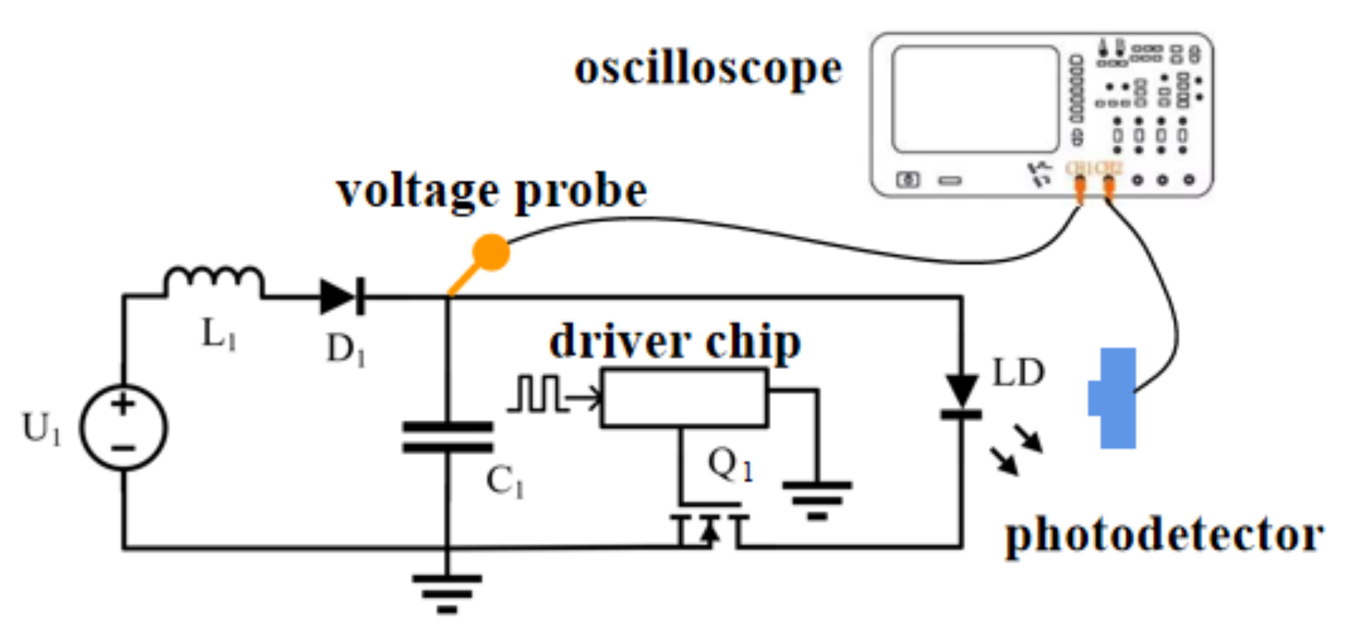
Based on the above design ideas, the schematic diagram of the laser diode drive circuit and the test platform are shown in Figure 2. is the energy storage capacitor. is an inductor used to limit current and provide higher voltage on . is a high-speed diode (1N4148). is an enhancement mode power transistor (EPC2019 from Efficient Power Conversion Corporation). is a semiconductor laser diode SPL DS90A_3 from OSRAM. The value of and will be discussed in Section 2.3.
In the test platform, a voltage probe is added to capacitor to record its voltage waveform, and a photodetector is added in front of the output port of the laser diode to receive the laser pulses. An oscilloscope is used to record the voltage waveform on and the output laser pulse waveform. All the following experiments are carried out on this test platform.
2.2. Circuit Working Stage
The laser drive circuit in this article is mainly divided into two working stages: discharging stage and charging stage.
Discharging stage. When is fully charged, and the GaN FET is turned on, begins to discharge through and , which produces a laser pulse. The discharging current path is shown in Figure 3a. When is turned on, the DC source also forms another loop through , , and —this current path is shown in Figure 3b. Due to the existence of the current limiting inductor , the current in this loop will be relatively small in a short switch conducting time, and the impact on the laser pulse can be ignored.
Charging stage. When is turned off, charges through and , the charging current path is shown in Figure 4. Besides charging , the current in Figure 3b also charges after is turned off. Although this DC current in Figure 3b is not very large, the capacitance value of is small, so the DC current can significantly increase the voltage on . When the other parameters of the circuit are unchanged, the magnitude of this DC current and the voltage on is controlled by the turn-on time of . Thus, the modulation of the discharging current and the peak power of the laser pulse can be achieved. The specific modulation method will be discussed later in Section 4.3.
In order to facilitate understanding, the timing diagram of circuit working process is shown in Figure 5. The discharging stage and charging stage correspond to the and of . During –, the laser diode emits laser pulse and there is a large pulse current, and the capacitor is completely discharged during this period. During –, the laser diode no longer emits laser pulse, and the DC current in Figure 3b keeps increasing. When is turned off, the capacitor is charged by and during –. – is the waiting time after is completely charged.
2.3. Circuit Analysis and Device Selection
In the nanosecond laser drive circuit, the influence of parasitic parameters on the circuit characteristics cannot be ignored, the actual circuit schematic with parasitic parameters is shown in Figure 6. is the parasitic resistance of the charging circuit. and is the parasitic inductance and resistance of the discharging circuit. For the convenience of analysis, in the dotted frame, the laser diode is equivalent to a model of a resistor in series with an inductor .
When is turned on, the discharge circuit through , , , LD ( and ) and can be regarded as an RLC circuit and the loop equation is:
The damping coefficient is defined as :
In order to obtain a laser pulse of narrow pulse width and high peak power, the RLC discharge circuit must work in underdamped conditions and . The discharge current in the LD is as follows:
Here, represents the amplitude of the current in the circuit. In order to obtain narrow pulse width and rapid rising edge, the frequency should be relatively large. Therefore, it is better to take a small value of , but when is very small, it can be known from (5) that the current amplitude is also very small, which cannot meet the requirement of high peak power of the laser pulse. This comes back to what was said at the beginning of the article. It is difficult to meet the requirements of high peak power and narrow pulse width at the same time. A suitable capacitor value should be chosen to achieve a balance. Finally, through calculation and experiment verification, we chose the value of as 1 nF. When the value of remains unchanged, a small inductance is required to make relatively large. Here, contains not only the equivalent inductance of LD, but also the parasitic inductance of the discharge circuit (). Usually, the equivalent inductance of LD is constant, so we need to reduce the parasitic inductance of the discharge circuit as much as possible.
Circuit parasitic inductance is mainly caused by PCB wiring and device packaging. Therefore, when designing PCB layout, the discharge current path should be designed as small as possible and further reduce the parasitic inductance by means of multiple discharge circuits in parallel [11], magnetic flux offset [12], etc. Different device packages also have great influence on the parasitic inductance of the circuit [13]. The laser diodes that use Transistor Outline Package will cause more parasitic inductance on their pins. Therefore, it is better to use a laser diode with a bare die for narrow pulse drive circuits. In this manuscript, the laser diode we use is SPL DS90A_3 from OSRAM. It is a bare die and is connected to the PCB by metal wire bonding.
The selection of switch also has a great influence on the output laser pulse. The switching speed and the maximum allowable current of will directly determine the pulse width and the peak power of laser pulse. Finally, considering switching speed, maximum allowable voltage, maximum allowable current and many other factors, we chose EPC2019, a GaN enhancement mode power transistor from EPC corporation.
The 3D model of the drive circuit discharging part is shown in Figure 7a. A single-layer capacitor is used as the discharge capacitor, which is connected to the input voltage and the laser diode by wire bonding. Figure 7b shows the real photo view of the discharging circuit board. The pulse discharging current path is designed to be as small as possible through the arrangement of the devices. In the laser drive circuit designed in this article, we used packaged GaN FETs, but in the future, if bare die GaN FETs are used, it will be possible to further reduce the length of the discharge current path, thereby reducing the parasitic inductance of the discharge circuit and reducing the pulse width of the laser pulse.
Figure 7 only shows the pulse discharging part of the drive circuit. The other modules of the circuit are designed to be placed on another circuit board. The purpose is to reduce the size of the core module and make it suitable for a Lidar system. The size of this discharging board is 4.3 mm × 6 mm.
3. Parameter Measurement and Verification
In the design of the laser drive circuit, the discharge current through the laser diode is a very important parameter. A series of information such as the peak power, pulse width and photoelectric conversion efficiency of the laser diodes are all inseparable from the measurement of discharge current waveforms. At the same time, the parasitic parameters in the discharge circuit can also be obtained by the discharge current waveforms, which provides a basis for circuit analyses and optimization.
Often, a sampling resistor is added to the discharge circuit to obtain the discharge current waveforms. In our previous experiments, we also adopted this scheme. However, the current waveforms obtained by sampling resistor have some problems. Figure 8 shows the comparison between the discharge current waveform measured by sampling resistor and the laser pulse waveform by photodetector.
Theoretically, the laser pulse waveform should be consistent with the shape of the discharge current waveform. However, in Figure 8 the pulse width of the discharge current is significantly wider than the pulse width of the laser pulse. This is mainly because the sampling resistor itself has a certain amount of inductance and the measuring probe will also bring contact resistance and inductance. It not only makes the pulse width of the measured discharge current larger, but also renders the amplitude larger. Meanwhile, the sampling resistor itself and more PCB trace length will bring more parasitic parameters to the discharging circuit and increase the pulse width of the laser pulse. It is inconsistent with the basic rules of laser drive circuit design. Therefore, the current in the discharge circuit cannot be measured directly by sampling resistor. However, when the conducting time of is very short, the current in Figure 3b is very small. Most of the discharge current in Figure 3a is provided by capacitor . It is easy to obtain the voltage waveform on by the voltage probe, and compared with the voltage value on the sampling resistor measured by the probe, the voltage value on is much larger, which can effectively reduce the measurement error caused by the parasitic parameters of the probe. Then, the discharge current can be obtained by differentiating the voltage waveform on when is turned on:
Figure 9 shows the voltage waveform measured on capacitor and the discharge current waveform obtained by differentiating the voltage waveform from (6). The input voltage was set as 30 V. of was set as 60 ns and the PPS was set as 1 kHz. The value of energy storage capacitor C1 was 1 nF.
When using a voltage probe to measure the voltage on the capacitor , the voltage waveform obtained is not ideal and stable, and there will be a certain noise signal. The magnitude of the discharge current is related to the slope of the voltage waveform on , especially when the slope of the voltage waveform is close to 0, the slope change caused by noise will cause the discharge current to repeatedly change around 0, so there will be negative discharge current waveforms in Figure 9. This is an error caused by measurement noise, and there is no negative discharge current in the actual circuit.
Theoretically, the shape of the emitted laser pulse waveform is consistent with the shape of the pulse current waveform passing through the laser diode. Figure 10 shows the comparison between the discharge current waveform obtained by differentiation and the laser pulse waveform detected by the photodetector. It can be seen that the pulse widths of the two waveforms are almost the same. Meanwhile, we measured the peak power of the laser pulse to be 121.1 W. Compared with the P-I diagram in the laser diode’s (SPL DS90A_3) datasheet, the maximum discharge current at this time should be about 35 A, which is similar to the discharge current waveform obtained by differentiation. Therefore, the discharge current waveform can be obtained by differentiating the voltage waveform on , and this measurement method is reliable.
Since the parasitic parameters of the drive circuit have a great influence on the pulse width and peak power of the laser under the working conditions of nanosecond pulse, it is necessary to obtain the parasitic parameters of the circuit through simulation analysis and experiments, especially the parasitic inductance and the parasitic resistance in the discharge circuit.
The simulation model of the drive circuit was established based on the schematic diagram of the circuit with parasitic parameters in Figure 6. The inductance and resistance in the discharge circuit are mainly composed of PCB traces and the equivalent parameters of the laser diode. Generally, the inductance of the laser diode itself is negligible compared with the parasitic inductance of the PCB traces. The parasitic inductance of PCB traces can be estimated based on 1 nH per millimeter. In the actual circuit, the length of the PCB trace is about 0.9 mm, so is preset to 1 nH in the simulation. We chose Pspice to be the simulation tool. Then, we adjusted the value of the parasitic parameters to make the simulated current waveform similar to the experimentally measured waveform. The measured waveform is obtained by differentiating the voltage waveform on through Equation (6). Finally, we determined that , . Figure 11 shows the comparison between the simulated current waveform and the measured current waveform. The parasitic parameters involved in the simulation are summarized in Table 2.
4. Experiment and Results
Based on the above analysis, an experimental prototype has been made. The photo of the circuit board is shown in Figure 12, including the discharge circuit board mentioned in Figure 7 and an adapter board to the external ports. All the following experiments are carried out on this experimental circuit board.
4.1. Influence of Input Voltage
The input voltage is a very important factor affecting the output laser pulse. Figure 13 shows the variation of peak power and pulse width with different input voltages. of was set as 60 ns, and the PPS was set as 1 kHz. The value of energy storage capacitor was 1 nF. From Equations (3) and (5), we can see that the peak power of output laser pulse will increase linearly with the increase in input voltage. This rule applies when the input voltage is less than 30 V, but when the input voltage exceeds 30 V, the increase in peak power of the laser pulse slows down obviously. The laser diode SPL DS90A_3 has a maximum peak power of 130 W at 40 A current. When the input voltage exceeds 30 V, the current in the discharge circuit has reached 40 A (the saturation current of the laser diode), and the peak power will not increase at about 130 W.
In addition to the increase in peak power, we can also see that the pulse width of the laser pulse has increased. It is mainly caused by the GaN devices’ hot-electron effects [14,15,16,17,18]: electrons flowing from source to drain are significantly accelerated by the high electric field, some of the electrons will rush to the AlGaN/GaN layer or the buffer and be trapped in them. The electron density in the discharge area decreases, resulting in the increase in the ON-resistance of the GaN switch. With the increase in ON-resistance of , it can be seen from Equations (3) and (4) that the pulse width of the laser pulse increases.
4.2. Influence of Pulse per Second (PPS)
Since the Lidar system needs to have a high data sampling rate, the number of laser pulses emitted per second needs to be very large. Therefore, it is necessary to study the drive circuit’s characteristics at different PPS.
Figure 14 shows the variation of peak power and pulse width with different PPSs. The input voltage was set as 30 V. of was set as 60 ns, and the value of energy storage capacitor was 1 nF. With the increase in PPS, the peak power of the laser pulse decreases slightly, but the pulse width decreases significantly. The pulse width of the laser pulse at 400 kHz is about 30% lower than that at 1 kHz. There are two main reasons for this phenomenon.
Firstly, when PPS increases, the relative dielectric constant of the capacitor will decrease [19]. The formation of dielectric constant is mainly caused by polarization, and the polarization is caused by the directional arrangement of certain dipoles. When the voltage on capacitor changes, the dipole will reverse with change of the external field. When the frequency is high, due to the resistance inside the material, the dipole reverses and cannot keep up with the speed of the electric field, and a kind of relaxation is formed. As a result, the relative dielectric constant will decrease and the value of the capacitor in proportion to will also decrease. Theoretically, the waveform of the laser pulse and the discharge current waveform are consistent in shape. From Equations (3) and (4) of the previous analysis of the discharge current, the waveform of the discharge current can be approximately regarded as a sinusoidal waveform, and the pulse width (50% of the rising edge to 50% of the falling edge) of the laser pulse can be expressed as:
When the value of C1 decreases, the pulse width of the current waveform and the laser pulse will both decrease. At the same time, it can be seen from Equations (3) and (5) that the amplitude of discharge current and the peak power of the laser pulse will decrease.
Secondly, when PPS of the drive circuit is very high, the switching loss and the heat of the laser diode cannot be ignored, and they will raise the temperature of the devices. When the temperature rises, the electron migration speed of GaN switch is further increased and the switching speed is accelerated [20]. Therefore, the pulse width of the laser pulse is narrowed.
When the devices temperature increases, the pulse width of the laser pulse can be reduced, but it does not mean that the system is suitable for high-temperature operation. Working at high temperatures for a long time does great harm to the life of the devices. In the experiment, we measured the temperature of the drive circuit working at 400 kHz PPS for a long time, which was over 80 ℃. It is necessary to add an auxiliary cooling device to the drive circuit when working at high PPS.
4.3. Power Modulation
In the previous analysis, we knew that we could change the voltage on the energy storage capacitor by changing the of , thus changing the peak power of laser pulse. In the application of a Lidar system, it usually needs to emit laser pulses and receive the reflected signals to obtain target objects. The reflected signal power is proportional to the transmission power. For the detection of long-distance targets, it is necessary to emit laser pulses with high peak power to meet the long-distance requirement. However, for the short-distance target objects, considering the input saturation of the photodetector at the receiving port and the safety of human eyes, it is necessary to reduce the peak power of the output laser pulse. Therefore, the modulated laser drive circuit is meaningful.
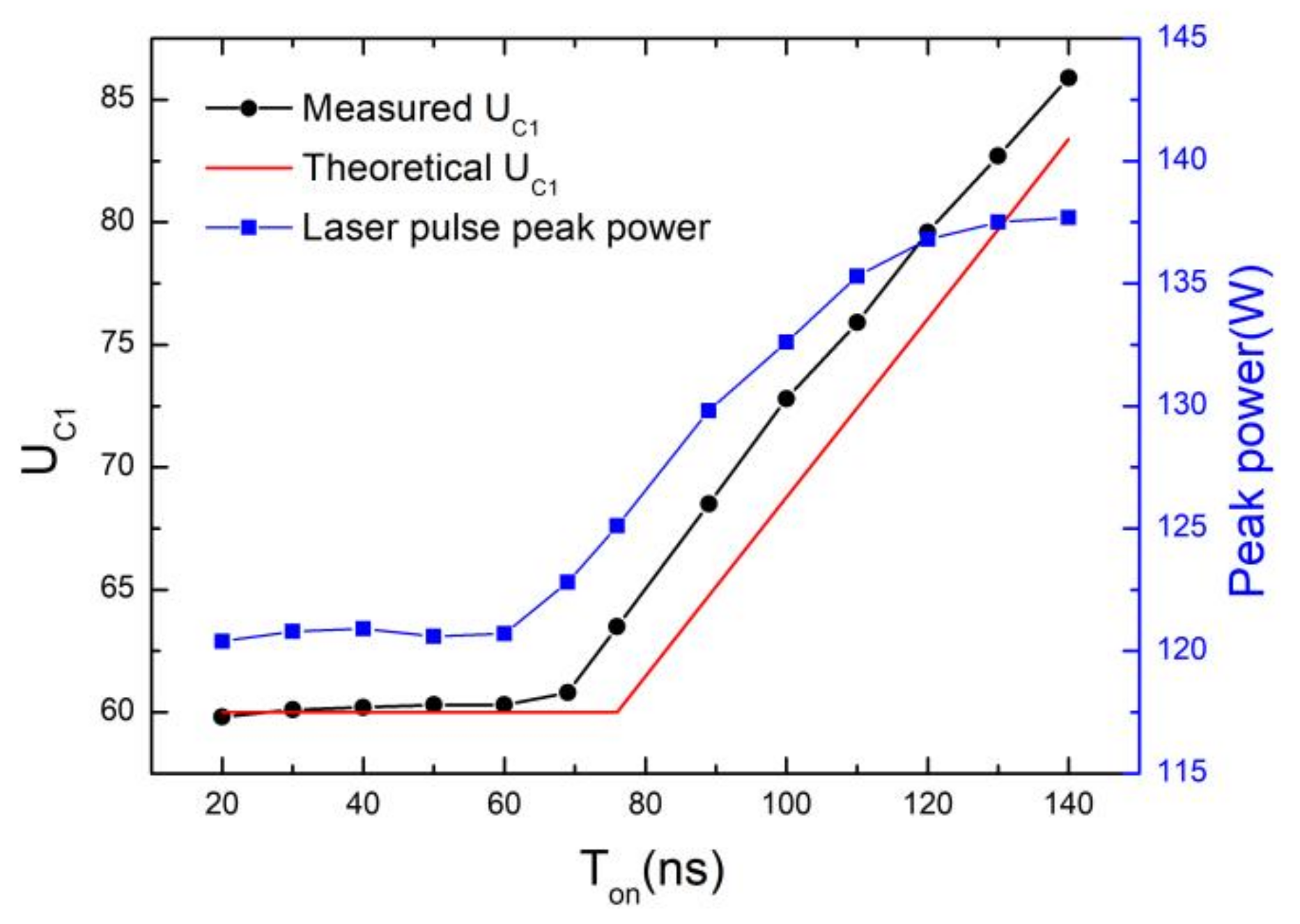
The input DC source voltage was set as 30 V and the PPS was set as 1 kHz. The discharge voltage on and the peak power of the laser pulse vary with the turn-on time of , as shown in Figure 15. When of is less than 60 ns, the maximum voltage on is almost unchanged, of course the peak power of the laser pulse also remains unchanged. When of exceeds 60 ns, the maximum voltage on will increase approximately linearly with the increase in . However, the increase in laser pulse peak power is nonlinear, mainly because the peak power of the laser pulse has exceeded 135 W, reaching the saturation power of the laser diode, and the power no longer increases.
The expression of the voltage on can be derived as follows. The duration of the process in Figure 3b is , and the charging time in the process in Figure 4 is . For the inductor , the following relationship can be obtained:
Therefore, the expression of the capacitor voltage can be obtained:
is the voltage of the input DC source. The charging time (10% of the rising edge to 90% of the rising edge) of the circuit is only related to the inductance , the capacitance and the parasitic parameters of the charging circuit. For the same circuit, these values do not change, so is a constant. Neglecting the parasitic resistance of the charging circuit, can be expressed as:
Since the charging time does not change in the same circuit, the final charging voltage on the capacitor is only depends on the conducting time . Additionally, due to the existence of the external DC source , when , the DC source will directly charge to twice of . This is why the voltage of in Figure 15 did not rise at the beginning. can be expressed in Equation (11).
In Figure 15, the reason why the measured value of does not completely coincide with the theoretical value is mainly caused by the difference in . calculated according to Equation (10) is 76 ns, here and are the actual values of the devices in Figure 6. Additionally, in our experiment, the actual measured charging time is 69 ns. Since we measured 10–90% of the rising edge of the waveform, will be less than the theoretical value. In other application scenarios, the appropriate and can be selected to change the value of to meet other modulation requirements.
Based on this modulation method of the capacitor voltage , a series of trigger signals with varying pulse widths can be generated through FPGA to obtain laser pulses with variable peak power. If the laser pulses with variable peak power are arranged according to a certain rule, a laser pulse train of arbitrary waveform can be obtained. Figure 16 is an example of the sinusoidal pulse train obtained in the experiment. The ordinate in the figure represents the output voltage of the photodetector, which is positively correlated with the power of the laser pulse. Each line in the waveform is composed of a laser pulse. The conducting time of the laser pulse with the minimum peak power is 60 ns, and for each subsequent pulse, is increased by 4 ns until the of the laser pulse with the maximum peak power is 120 ns. Additionally, then, is reduced to 60 ns with 4 ns less per pulse to form a complete cycle. The time interval between each laser pulse is 1 μs.
Based on the Equation (11), the input DC source voltage in the experiment is 30 V, so the voltage on is at least 60 V, which makes the current in the discharge circuit close to the saturation current of the laser diode. As a result, the modulation range of the laser pulse peak power is relatively small. If a smaller input voltage is chosen, a larger range of laser pulse peak power modulation can be achieved in this way.
In a Lidar system, this modulation method for the laser diode light source has many advantages. Firstly, the peak power of the laser pulse can be modulated only by changing the pulse width of the input trigger signal without changing the input voltage, and the pulse width modulation of input trigger signal can be easily realized by FPGA. Meanwhile, the pulse width and PPS of the input trigger signal can be continuously modulated, which means that in a laser pulse train, the peak power and PPS of each laser pulse can be controlled. In addition, this modulation method can also be used in many other fields, such as laser communication, laser scanning imaging, and face recognition.
5. Conclusions
A semiconductor laser drive circuit for TOF Lidar system is designed and tested in this manuscript. It is necessary to obtain the laser pulse with narrow pulse width and high peak power to detect further distances and obtain a higher detection accuracy. In order to reduce the pulse width, the discharge current path on the PCB is minimized as much as possible to reduce the parasitic inductance, and some specially packaged components and connecting methods are used. GaN devices are used to improve the switching speed and reduce the switching loss. The drive circuit and the laser pulse characteristics was tested under different working conditions, where the influence of circuit parasitic parameters, the GaN devices’ dynamic switching characteristics and the influence of temperature need to be considered. Finally, the peak power of the laser pulse can reach 135 W, and the pulse width is less than 2 ns at the PPS of 400 kHz. Compared with other existing research results, the levels of various parameters have been greatly improved: the pulse width has been reduced by 70% and the number of pulses per second has been increased by 10 times. Meanwhile, the laser pulse peak power modulation method has been proposed to meet the requirements of the Lidar system in different application scenarios.
Author Contributions
Conceptualization, Z.C. and Y.Y.; data curation, Z.C.; investigation, Z.C. and Y.Y.; methodology, Z.C., J.S., K.L. and J.Q.; project administration, K.L. and J.Q.; software, J.S.; writing—original draft, Z.C.; writing—review and editing, K.L. and J.Q. All authors have read and agreed to the published version of the manuscript.
Funding
This research was funded by Fudan University and Changchun Institute of Optics Joint Foundation, grant number FC2017-002.
Conflicts of Interest
The authors declare no conflict of interest. The funders had no role in the design of the study; in the collection, analyses, or interpretation of data; in the writing of the manuscript, or in the decision to publish the results.
References
- Gavalas, D.; Pantziou, G.; Konstantopoulos, C.; Mamalis, B. LIDAR: A protocol for stable and energy-efficient clustering of ad-hoc multihop networks. Telecommun. Syst. 2007, 36, 13–25. [Google Scholar] [CrossRef]
- Takai, I.; Matsubara, H.; Soga, M.; Ohta, M.; Ogawa, M.; Yamashita, T. Single-Photon Avalanche Diode with Enhanced NIR-Sensitivity for Automotive LIDAR Systems. Sensors 2016, 16, 459. [Google Scholar] [CrossRef] [PubMed]
- Horaud, R.; Hansard, M.E.; Evangelidis, G.D.; Ménier, C. An overview of depth cameras and range scanners based on time-of-flight technologies. Mach. Vis. Appl. 2016, 27, 1005–1020. [Google Scholar] [CrossRef] [Green Version]
- Kilpelä, A.; Kostamovaara, J. Laser pulser for a time-of-flight laser radar. Rev. Sci. Instrum. 1997, 68, 2253–2258. [Google Scholar] [CrossRef] [Green Version]
- Soulard, R.; Quinn, M.N.; Tajima, T.; Mourou, G. ICAN: A novel laser architecture for space debris removal. Acta Astronaut. 2015, 105, 192–200. [Google Scholar] [CrossRef]
- Wen, S.; Wang, M.; Xie, J.; Wu, D. Large current nanosecond pulse generating circuit for driving semiconductor laser diode. Microw. Opt. Technol. Lett. 2019, 61, 867–872. [Google Scholar] [CrossRef]
- Xu, X.; Zhang, H.; Zhang, X. Design of High-frequency and Narrow Pulsed Driver Power of Laser Fuze. Acta Photonica Sinica 2017, 46, 114002. [Google Scholar]
- Wenzel, H.; Klehr, A.; Liero, A.; Christopher, H.; Fricke, J.; Maaßdorf, A.; Zeghuzi, A.; Knigge, A. High pulse power wavelength stabilized 905 nm laser bars for automotive LiDAR. In Proceedings of the 2019 IEEE High Power Diode Lasers and Systems Conference (HPD), Coventry, UK, 9–10 October 2019. [Google Scholar]
- Hu, C.; Qin, S.; Wang, X. An extremely fast and high-power laser diode driver module. In Semiconductor Lasers and Applications II, Proceedings of the PHOTONICS ASIA 2014, Beijing, China, 8–11 November 2004; Yao, J., Chen, Y., Lee, S., Eds.; SPIE: Bellingham, WA, USA, 2005. [Google Scholar]
- Zhang, W.; Hao, Q.; Song, Y.; Shang, F.; Sun, H.; Li, T. A High Power Laser Diode Driver and Collimating Optical System Design for Laser 3D Imaging. In Semiconductor Lasers and Applications V, Proceedings of the PHOTONICS ASIA 2012, Beijing, China, 5–7 November 2012; Zhu, N., Li, J., Peters, F.H., Yu, C., Eds.; SPIE: Bellingham, WA, USA, 2012. [Google Scholar]
- Texas Instruments. Nanosecond Laser Driver Reference Design for LiDAR. Available online: http://www.ti.com/tool/TIDA-01573 (accessed on 26 February 2021).
- Reusch, D.; Strydom, J. Understanding the Effect of PCB Layout on Circuit Performance in a High-Frequency Gallium-Nitride-Based Point of Load Converter. IEEE Trans. Power Electron. 2014, 29, 2008–2015. [Google Scholar] [CrossRef]
- Yan, Y.; Chen, Z.; Qiu, J.; Liu, K. Effect of Package on Electroluminescence Characteristics of Vcsel Under Short Pulse and Large Current. Acta Optica Sin. 2020, 40, 0814001. [Google Scholar]
- Persson, E. Practical application of 600V GaN HEMTs in power electronics. In Proceedings of the 2015 IEEE Applied Power Electronics Conference and Exposition (APEC), Charlotte, NC, USA, 15–19 March 2015. [Google Scholar]
- Li, R.; Wu, X.; Xie, G.; Sheng, K. Dynamic on-state resistance evaluation of GaN devices under hard and soft switching conditions. In Proceedings of the 2018 IEEE Applied Power Electronics Conference and Exposition (APEC), San Antonio, TX, USA, 4–8 March 2018; pp. 898–903. [Google Scholar]
- Li, K.; Evans, P.L.; Johnson, C.M. Characterisation and modeling of gallium nitride power semiconductor devices dynamic on-state resistance. IEEE Trans. Power Electron. 2018, 33, 5262–5273. [Google Scholar] [CrossRef] [Green Version]
- Cai, Y.; Forsyth, A.J.; Todd, R. Impact of GaN HEMT dynamic on-state resistance on converter performance. In Proceedings of the 2017 IEEE Applied Power Electronics Conference and Exposition (APEC), Tampa, FL, USA, 26–30 March 2017; pp. 1689–1694. [Google Scholar]
- Binari, S.; Klein, P.; Kazior, T. Trapping effects in GaN and SiC microwave FETs; Institute of Electrical and Electronics Engineers (IEEE): Torino, Italy, 2002; Volume 90, pp. 1048–1058. [Google Scholar]
- Wang, Z.; Wu, X.; Feng, S.; Lin, L. Research on frequency characteristics of permeability and permittivity of La_(1-x)Sr_xMnO_3 Oxide. J. Chinese Rare Earth Soc. 2006, 24, 310–313. [Google Scholar]
- Zhang, Z.; Guo, B.; Wang, F.; Tolbert, L.M.; Blalock, B.J.; Liang, Z.; Ning, P. Methodology for switching characterization evaluation of wide band-gap devices in a phase-leg configuration. In Proceedings of the 2014 IEEE Applied Power Electronics Conference and Exposition (APEC), Fort Worth, TX, USA, 16–20 March 2014; pp. 2534–2541. [Google Scholar]
Figure 1.
Laser drive circuit structure.

Figure 2.
Schematic diagram of the laser diode drive circuit and the test platform.

Figure 3.
(a) Discharging current path during discharging stage; (b) DC current path during discharging stage.
Figure 3.
(a) Discharging current path during discharging stage; (b) DC current path during discharging stage.

Figure 4.
Current path during charging stage.

Figure 5.
Timing diagram of circuit working process.

Figure 6.
Actual circuit schematic with parasitic parameters.

Figure 7.
(a) 3D model of the drive circuit discharging part; (b) a real photo of the circuit board.
Figure 7.
(a) 3D model of the drive circuit discharging part; (b) a real photo of the circuit board.

Figure 8.
The comparison between the discharge current waveform measured by sampling resistor and the laser pulse waveform detected by the photodetector.
Figure 8.
The comparison between the discharge current waveform measured by sampling resistor and the laser pulse waveform detected by the photodetector.

Figure 9.
The voltage waveform on capacitor and the discharge current waveform obtained by differentiating the voltage waveform.
Figure 9.
The voltage waveform on capacitor and the discharge current waveform obtained by differentiating the voltage waveform.

Figure 10.
The comparison between the discharge current waveform obtained by differentiation and the laser pulse waveform detected by the photodetector.
Figure 10.
The comparison between the discharge current waveform obtained by differentiation and the laser pulse waveform detected by the photodetector.

Figure 11.
Laser pulse waveform, discharge current waveform obtained by differentiation (measured waveform), and simulated discharge current waveform.
Figure 11.
Laser pulse waveform, discharge current waveform obtained by differentiation (measured waveform), and simulated discharge current waveform.

Figure 12.
The photo of the experimental prototype.

Figure 13.
Variation of laser pulse peak power and pulse width at different input voltages.

Figure 14.
Variation of laser pulse peak power and pulse width at different pulses per second (PPSs).
Figure 14.
Variation of laser pulse peak power and pulse width at different pulses per second (PPSs).

Figure 15.
Variation of voltage on and laser pulse peak power at different .

Figure 16.
An example of power modulation.


Table 1.
Recent research results of semiconductor laser drive circuits.
| Reference | Peak Power | Pulse Width | Pulse per Second |
|---|---|---|---|
| [7] | 70 W | 20 ns | 30 kHz |
| [8] | 100 W | 10 ns | 10 kHz |
| [9] | 50 W | 8 ns | 10 kHz |
| [10] | 150 W | 14 ns | 1 kHz |
| Drive circuit in this manuscript | 135 W | 2 ns | 400 kHz |
Table 2.
Parasitic parameters involved in the simulation.
| Designator | Description | Value |
|---|---|---|
| Parasitic inductance of the discharge circuit | 1.1 nH | |
| Parasitic resistance of the discharge circuit | 0.5 Ω | |
| Equivalent inductance of the laser diode | In series with | |
| Equivalent resistance of the laser diode | In series with |
Publisher’s Note: MDPI stays neutral with regard to jurisdictional claims in published maps and institutional affiliations. |
© 2021 by the authors. Licensee MDPI, Basel, Switzerland. This article is an open access article distributed under the terms and conditions of the Creative Commons Attribution (CC BY) license (https://creativecommons.org/licenses/by/4.0/).
Share and Cite
MDPI and ACS Style
Chen, Z.; Yan, Y.; Shu, J.; Liu, K.; Qiu, J. Modulated High Power and Narrow Pulse Width Laser Drive Circuit for Lidar System. Electronics 2021, 10, 823. https://doi.org/10.3390/electronics10070823
AMA Style
Chen Z, Yan Y, Shu J, Liu K, Qiu J. Modulated High Power and Narrow Pulse Width Laser Drive Circuit for Lidar System. Electronics. 2021; 10(7):823. https://doi.org/10.3390/electronics10070823
Chicago/Turabian StyleChen, Zhiwen, Yingying Yan, Jun Shu, Kefu Liu, and Jian Qiu. 2021. "Modulated High Power and Narrow Pulse Width Laser Drive Circuit for Lidar System" Electronics 10, no. 7: 823. https://doi.org/10.3390/electronics10070823
Note that from the first issue of 2016, this journal uses article numbers instead of page numbers. See further details here.