
Purification and Improved Photoelectric Properties of Lead-Free Perovskite Cs3Bi2Br9 Crystals
Tianjin Key Laboratory of Functional Crystal Materials, Institute of Functional Crystals, School of Materials Science and Engineering, Tianjin University of Technology, Tianjin 300384, China
*
Authors to whom correspondence should be addressed.
Crystals 2023, 13(6), 871; https://doi.org/10.3390/cryst13060871
Submission received: 9 May 2023
/
Revised: 23 May 2023
/
Accepted: 24 May 2023
/
Published: 26 May 2023
Abstract
:The lead-free halide perovskite Cs3Bi2Br9 is a promising semiconductor material for room-temperature X-ray detection due to its excellent properties. However, material purity and crystal quality still limit the use of Cs3Bi2Br9 crystals as detectors. In this work, we present a highly efficient purification method using continuous vacuum extraction to sublimate BiBr3 precursors for Cs3Bi2Br9. Impurity analysis via inductively coupled plasma mass spectroscopy showed that the purification method successfully removed most of the impurities in BiBr3 precursors and improved the purity by at least one order of magnitude. Centimeter-sized Cs3Bi2Br9 single crystals were grown by the vertical Bridgman method. The improved properties after purification were confirmed by UV-Vis-NIR spectra, infrared transmittance, and current–voltage (I–V) measurements. The results showed that the average transmittance of Cs3Bi2Br9 crystals significantly increased from 62% to 75% in the 0.5–20 μm spectral range. Additionally, the resistivity increased by nearly three orders of magnitude from 5.0 × 10⁹ Ω·cm to 2.2 × 10¹² Ω·cm, meaning the material will have low leakage currents and be suitable for developing applications for room temperature radiation detection.
1. Introduction
Bismuth-based halide perovskite crystals have sparked great interest due to their excellent physical properties and promising applications in X/γ-ray detection [1,2], photovoltaic devices [3,4], ultraviolet photodetectors [5,6], and light-emitting diodes [7,8], etc. As with most halide perovskite crystals, their photoelectric properties, such as resistivity, carrier mobility lifetime product (μτ), band gap, and optical transmittance, are strongly dependent on chemical impurities as well as crystalline quality. Therefore, purification techniques, such as the low-cost mass production of halide perovskite crystals with good properties, are in high demand. Over the past few decades, different purification techniques have been developed for the fabrication of high-quality crystals (zone refining method [9,10], physical vapor transport method-PVT [11,12,13], recrystallization [14,15]), which greatly improved the optical and electrical properties of crystals. Among these techniques, the PVT method is widely used because of its cost-effectiveness and simplicity. During the PVT process, the initial material is usually sealed in a quartz tube and placed in a high-temperature zone, while the purified material is deposited in a low-temperature zone. Zheng et al. [12] purified thallium bromide (TlBr) salt using the PVT method, and trace impurities after purification were reduced to the ppb/ppm level. The resistivity of the resultant TlBr crystals increased from 2.58 × 10⁸ Ω·cm to 3.98 × 10⁹ Ω·cm and the average infrared transmittance increased from 27% to 48%. Kwon et al. [13] analyzed Hg2Br2 powders purified by the PVT method and found that the purity of Hg2Br2 increased from 4 N (99.99%) to 5 N (99.999%). Subsequently, high-quality Hg2Br2 crystals with little lattice distortions were obtained using purified raw materials. Lin et al. [16] used the PVT method to remove most of the impurities in TlI4 raw materials, as evidenced by GDMS analysis, resulting in the growth of high-performance Tl6SI4 crystals with a high resistivity of 5 ×1 012 Ω·cm and a high electron mobility of 35 ± 7 cm2·V−1·s−1, achieving spectroscopic detection with an energy resolution of 27% for 241Am α-particles. It can be seen that removing impurities from raw materials using the PVT method can remarkably improve the photoelectric properties of semiconducting crystals. However, for raw materials with a low vapor pressure, the purification effectiveness of the PVT method is not sufficiently effective.
Bismuth-based halide perovskite Cs3Bi2Br9 crystals are the newly discovered promising candidates for X-ray detection due to their excellent properties [17,18]. Nevertheless, there are still great challenges in preparing low-cost, large-volume, high quality Cs3Bi2Br9 crystals for X-ray imaging systems. Herein, the purification technique was utilized to increase the purity of raw materials for the low-cost production of large-sized Cs3Bi2Br9 crystals with high performance. For Cs3Bi2Br9 crystals, the precursor reagents (BiBr3) have low vapor pressure [19], so a modified and high-efficient PVT method, namely the dynamic vacuum vapor transport method, was developed to purify the BiBr3 precursors, indirectly improving the purity of Cs3Bi2Br9 crystals. The effectiveness of this purification process was evaluated via trace elemental analysis of BiBr3 precursors before and after purification. In addition, single, centimeter-sized Cs3Bi2Br9 crystals were grown by the Bridgman method using the purified BiBr3 precursors to further assess the effectiveness of the purification method in improving optical and electric properties. The effective purification process applied to the BiBr3 precursors resulted in an increased purity of at least one order of magnitude, increased resistivity of two orders of magnitude, and increased optical transmittance from 62% to 75%.
2. Materials and Methods
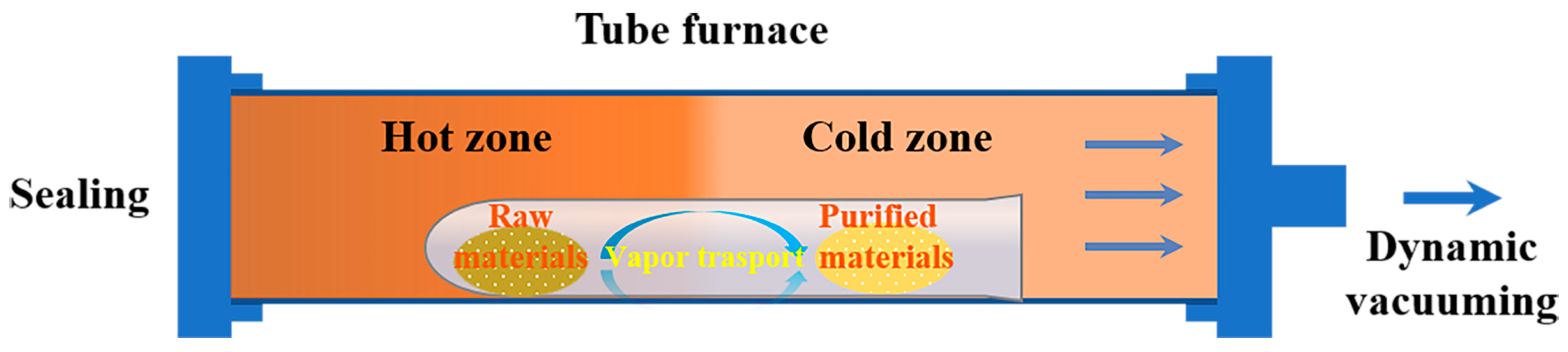
The precursors for the synthesis of Cs3Bi2Br9 polycrystals were CsBr and BiBr3. The purification of BiBr3 precursors can indirectly reduce impurities in Cs3Bi2Br9 crystals grown later. Because of the low vapor pressure of BiBr3, the conventional purification by physical vapor transport was not efficient enough for the purification of BiBr3. In this work, we proposed a new and modified vapor transport (dynamic vacuum vapor transport method (DVT)) for the purification of BiBr3. The DVT purification method differed from the traditional one in two aspects: the quartz ampule was not sealed and the furnace chamber providing the heat field was continuously vacuumed throughout the purification. It was worth noting that vacuuming was implemented from the cold end of the furnace. In this way, the raw materials were kept in a negative pressure environment (0.1–0.3 Pa) during the purification process, which greatly increased the sublimation rate of the raw materials so that the raw materials could be sublimated quickly at a low-temperature range (180–210 °C) to achieve the desired purification results. Figure 1 illustrates the principle of the DVT purification method. The detailed purification process of BiBr3 precursors using DVT is as follows. Commercial BiBr3 powders with a purity of 99% were loaded into the bottom of the quartz ampule in an argon-filled glovebox and then the ampule was fixed into a five-zone horizontal tube furnace to be subject to purification. The bottom and open end of the ampule were placed in the hot zone and cold zone, respectively. The temperature in the hot zone was below the melting point of BiBr3 and the temperature difference between these two zones was at least greater than 50 °C, which created a desirable temperature gradient. During purification, the furnace chamber was continuously vacuumed to less than 1 Pa, which markedly enhanced the sublimation and vapor transport of the BiBr3 powders. Finally, the purified BiBr3 was deposited near the open end of the ampule and collected for trace element analysis and crystal growth.
Before crystal growth, the quartz ampule with an inner diameter of 15 mm and a thickness of 2.5 mm was first cleaned with acetone, aqua regia, and deionized water, in turn. CsBr (3 N) powders and the purified BiBr3 with a molar ratio of 3: 2 were loaded into the cleaned ampule. The loaded ampule was sealed using an H2-O2 torch at a dynamic vacuum of 2–4 × 10⁻⁵ Pa and then placed in a rocking furnace where polycrystalline Cs3Bi2Br9 was synthesized at a soaking temperature of 650 °C. Subsequently, the ampule with polycrystalline Cs3Bi2Br9 was loaded into a six-zone growth furnace, and the growth program was run in the pre-designed temperature field with a growth temperature of 630–635 °C and a temperature gradient of 10–30 K/cm near the growth interface. During the growth, the translation rate of the heater was 0.8–1.5 mm/h. After growth, the furnace temperature was slowly cooled to room temperature to reduce the thermal stress that induced structural defects (cracks, dislocations, etc.).
The as-grown Cs3Bi2Br9 ingots were sliced perpendicular to the growth direction into wafers with dimensions of 5 × 5 × 2 mm3 using a diamond wire saw (STX-202A, KEJING, Shenyang, China). The wafers were mechanically polished using SiC sandpapers and water-free Al2O3 suspensions with a particle size of 0.03 μm to obtain a mirror surface for analysis. The optical properties of the polished samples were characterized by a UV-Vis-NIR spectrophotometer (UH4150, HITACHI, Tokyo, Japan) with a scanning range of 190–2500 nm and a Nicolet iS50 spectrometer (ThermoFisher, Waltham, MA, USA) with a scanning range of 500–4000 cm−1. Au electrodes were thermally evaporated on the top and bottom surface of the polished samples and then the I–V characteristic curves were obtained using a Keithley 6514B electrometer (Tektronix, Johnstown, OH, USA). The structure and crystalline quality of the grown Cs3Bi2Br9 crystals were investigated by X-ray diffraction with Cu-Kα1 radiation (XRD, Rigaku, Tokyo, Japan). In addition, impurities in BiBr3 precursors before and after purification were analyzed via inductively coupled plasma mass spectroscopy (ICP-MS, Agilent, Santa Clara, CA, USA) to evaluate the effectiveness of purification.
3. Results
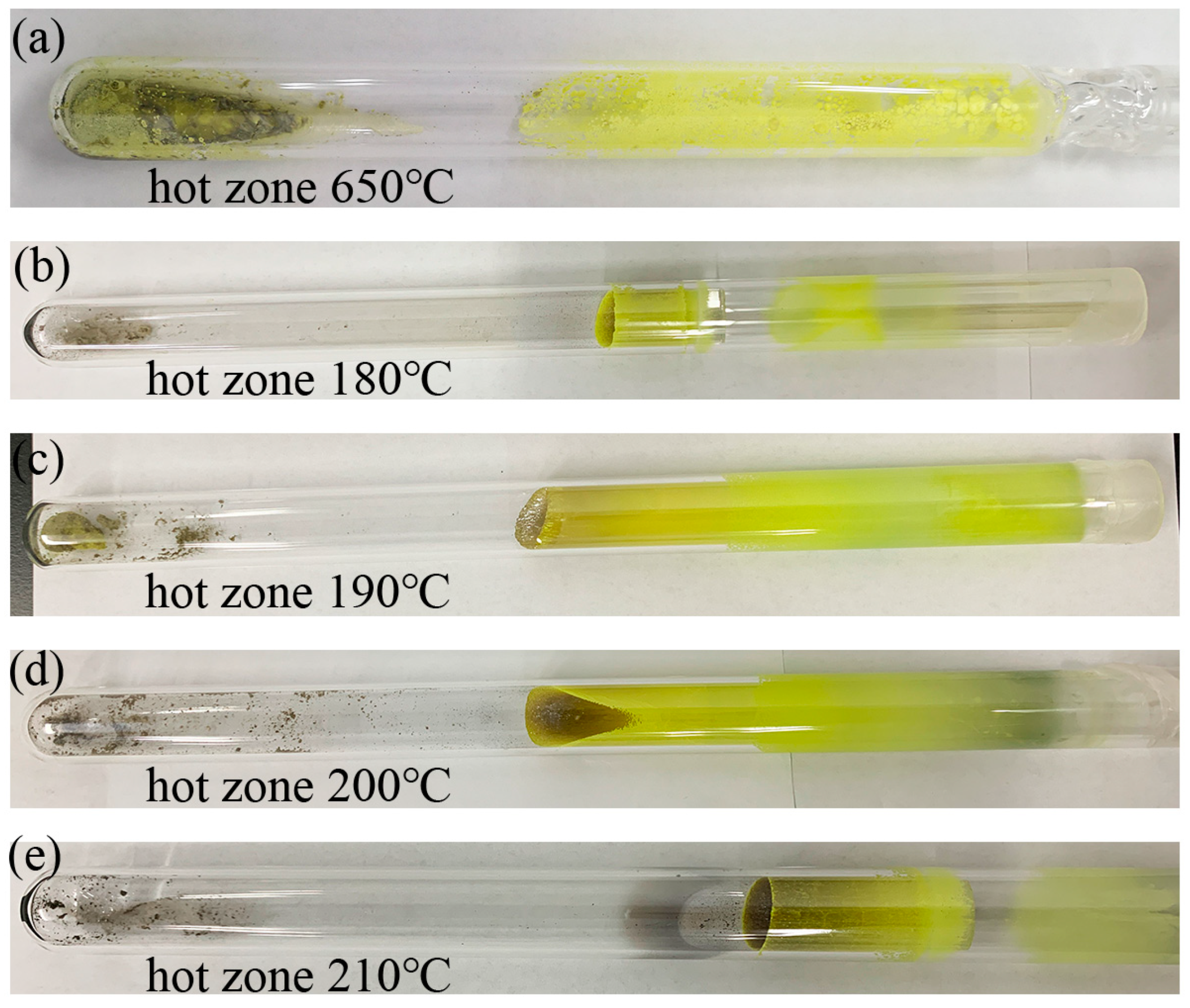
For comparison, the traditional physical vapor transport method was used to purify BiBr3 precursors. BiBr3 powders with a weight of 10 g were sealed in the quartz ampule with a vacuum of 2–4 × 10⁻⁵ Pa. During purification, the hot zone was set to 650 °C and held for 20 h, while the cold zone was set below the boiling point (462 °C) of BiBr3 to facilitate BiBr3 vapor transport. The results showed that only a small number of BiBr3 powders were vaporized due to their low vapor pressure, and they were deposited in the cold end region of the ampule (Figure 2a), meaning the purification effect was not achieved by the traditional physical vapor transport method. To increase the vapor transport of BiBr3 powders at low temperatures, the dynamic vacuum vapor transport method (DVT method) was developed to purify BiBr3, and the effect of temperature on purification was investigated. The hot zone was set to 180 °C, 190 °C, 200 °C, and 210 °C, respectively, while the cold zone was at least 50 °C lower than the hot zone. It turned out that BiBr3 powders with a weight of 10 g began to sublimate when the temperature in the hot zone reached 180 °C, and then sublimated completely after holding for 5 h. The gray impurities from the initial BiBr3 powders remained at the bottom of the ampule in the hot zone, while the purified BiBr3 transported by gasification was deposited near the open end of the ampule in the cold zone (Figure 2b). An optimal result was obtained when the temperature in the hot zone was increased to 190 °C. It took only 6 h to purify the BiBr3 with a weight of 20 g, and the color of BiBr3 deposited at the cold end was bright yellow (Figure 2c), indicating that its purity was improved. If the temperature was further raised to 200 °C or 210 °C, the purification time was shortened to less than 4 h, but a small number of impurities were also transported along with the BiBr3 vapor phase and deposited on the cold end (Figure 2d,e), which significantly deteriorated the purity of the raw materials.
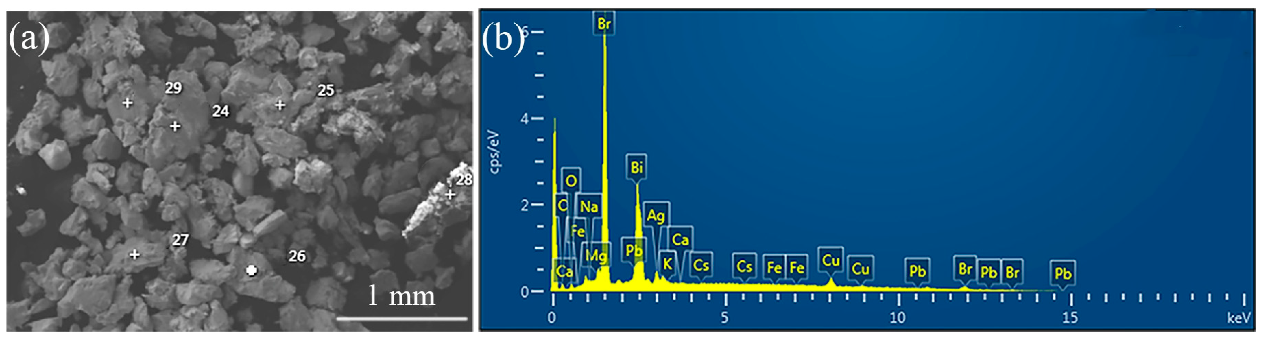
Table 1 shows impurity concentrations in BiBr3 precursors before and after purification using the DVT method. It shows that the DVT method is highly effective in eliminating impurity elements, Na, K, Ca, Mg, Al, Fe, Cu, Ag, and Pb. The concentration of P increased after purification, which is attributed to the high volatility of P impurity. Before purification, the total impurity concentration was 6649.14 ppm, and its corresponding purity was 99.33%. However, after purification, the total impurity concentration was sharply reduced to 727.24 ppm, and the corresponding purity was 99.93%, indicating that the purity of BiBr3 had improved by an order of magnitude. In addition, the gray residual impurities remaining after purification were analyzed by a scanning electron microscope with energy-dispersive X-ray spectroscopy (SEM-EDS, FEI, Portland, OR, USA), as shown in Figure 3. The impurity elements and their contents in the grey residues were shown in Table 2. As can be seen, five main impurities were identified: C, O, Cu, Ag, and Na. These impurities were not uniformly distributed in the grey residues, with average mass fractions of 7.09% (C), 1.87% (O), 5.49% (Cu), 2.84% (Ag), and 0.12% (Na), respectively. The results of the impurity analysis indicated that the DVT method was quite effective in removing impurity elements, C, O, Cu, Ag, Na, K, Ca, Mg, Al, Fe, and Pb, and could improve the purity of BiBr3 by at least one order of magnitude, which would substantially decrease impurities in the resultant Cs3Bi2Br9 crystals.
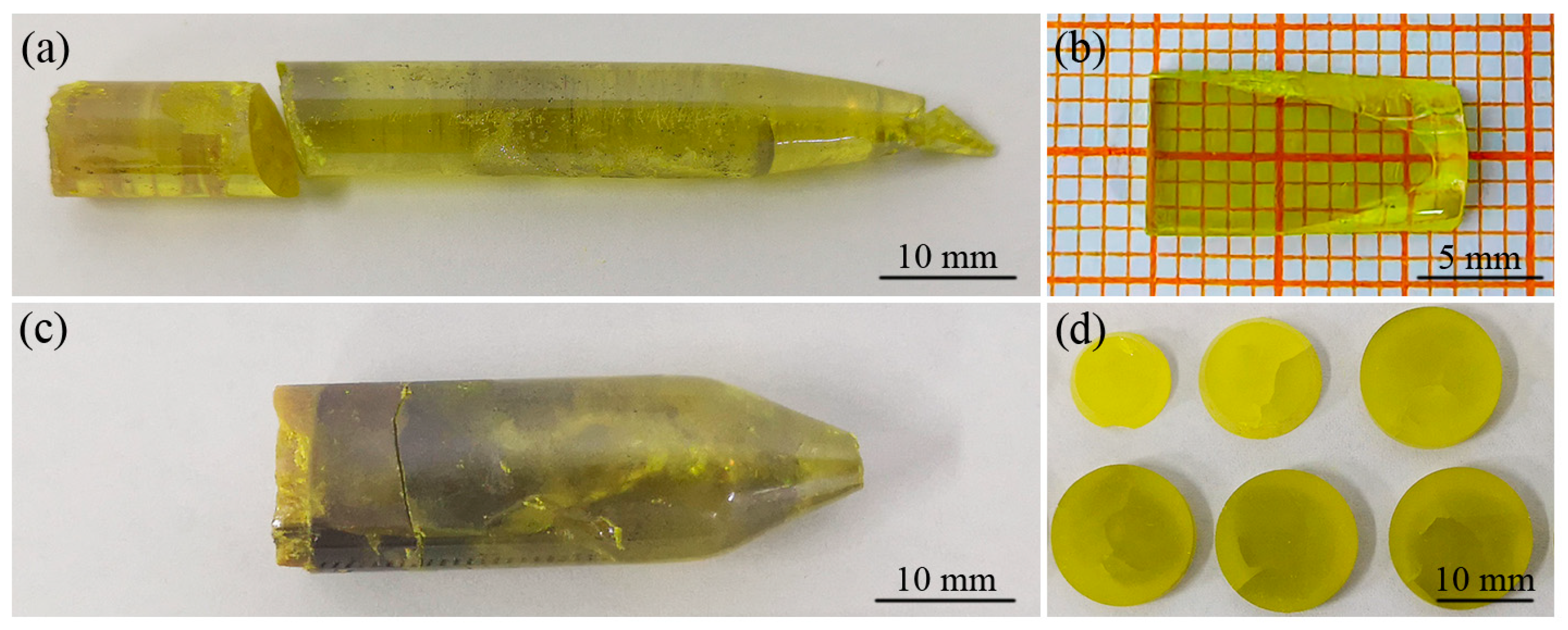
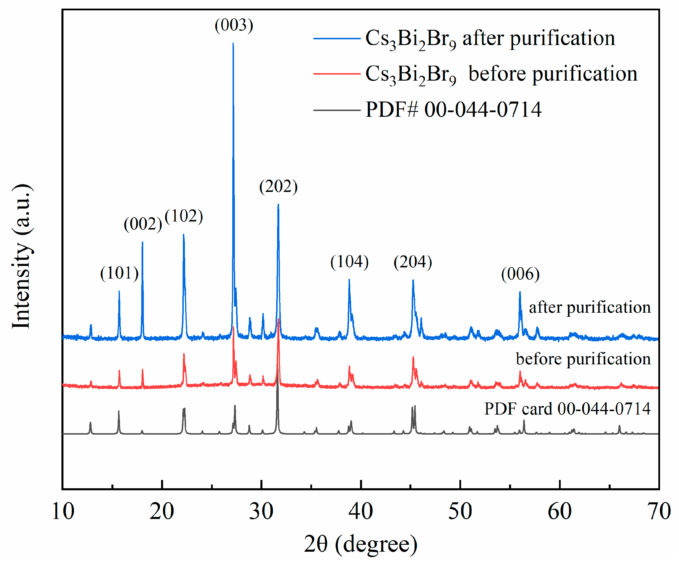
Polycrystalline Cs3Bi2Br9 was synthesized by a direct, stoichiometric chemical reaction of CsBr and BiBr3 precursors and then used for crystal growth in a vertical Bridgman furnace. Figure 4a shows a single Cs3Bi2Br9 crystal ingot with a diameter of 8 mm and a length of about 60 mm, grown by the Bridgman method using the purified BiBr3 precursors. It can be seen that the ingot was transparent under ambient light, and the bright yellow color of the entire ingot was uniform (Figure 4a,b), suggesting that the grown crystals may have a good crystalline quality. However, using the unpurified BiBr3 precursors, the grown Cs3Bi2Br9 ingot with a diameter of 15 mm and a length of about 50 mm was polycrystalline and appeared opaque under ambient light (Figure 4c). The color of the ingot was inhomogeneous, being bright yellow at the tip and dark yellow at the tail (Figure 4d). The color inhomogeneity and the appearance of grain boundaries were attributed to impurities and their segregation occurring in the melt during crystal growth. A similar result was observed by Hayashi [11] et al. In addition, XRD patterns of the grown Cs3Bi2Br9 crystals are shown in Figure 5, and all diffraction peaks were consistent with the standard PDF card (number: 00-044-0714), indicating that the grown crystals have a high phase purity and hexagonal structure. However, it was worth noting that the intensity of the diffraction peaks was significantly enhanced for the purified crystals, which generally indicates that the crystal has a good crystalline quality [20,21,22]. Therefore, these results demonstrated that it was beneficial to obtain single, high-quality, transparent Cs3Bi2Br9 crystals by purifying BiBr3 precursors to reduce impurities.
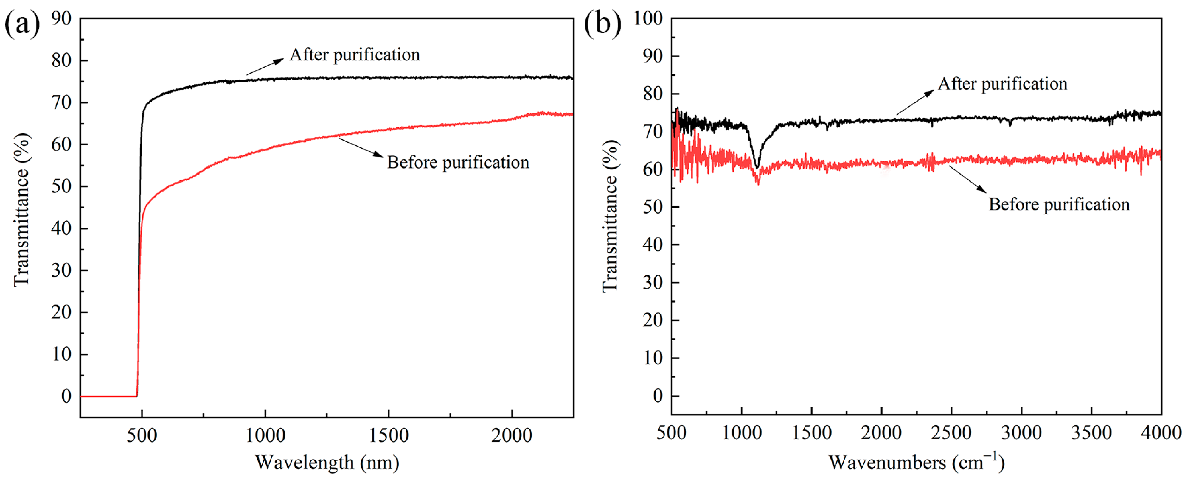
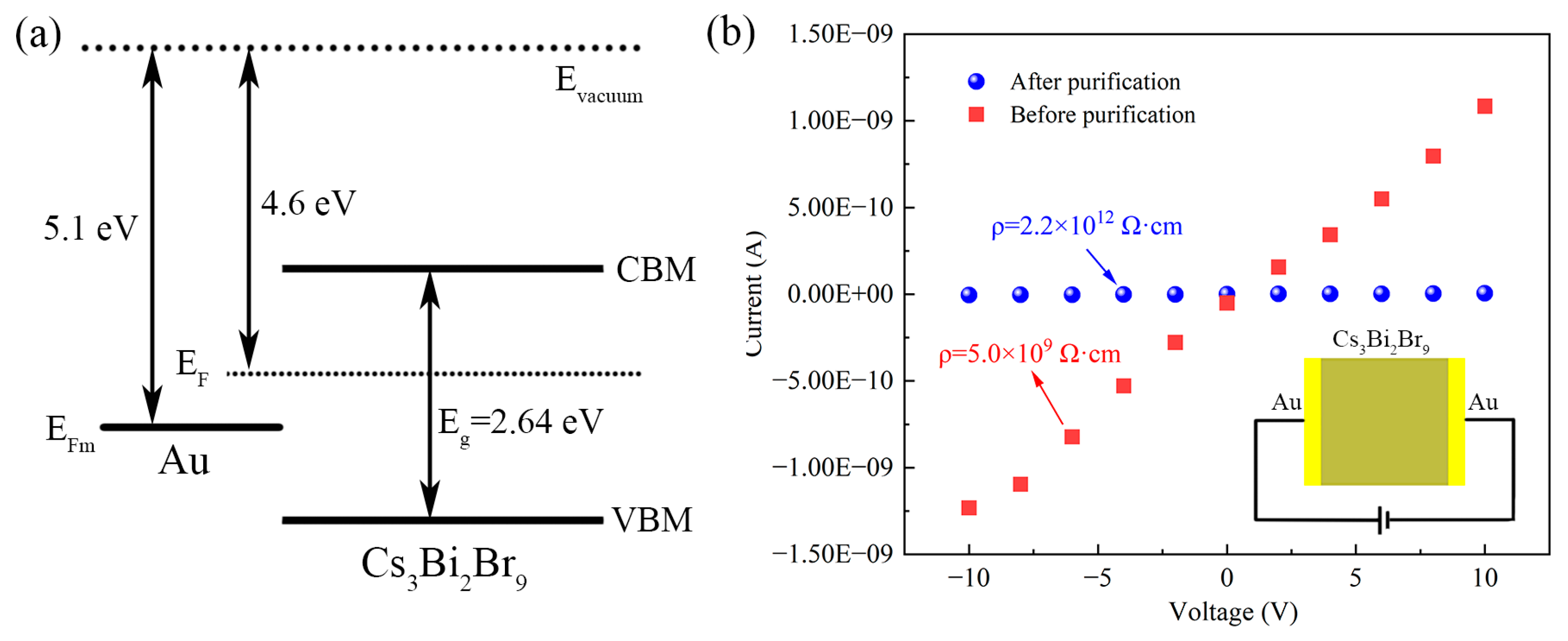
The optical characteristics of the grown Cs3Bi2Br9 crystals in the wavelength range of 0.2–20 μm are shown in Figure 6. The UV-Vis-NIR spectra showed that the purified Cs3Bi2Br9 crystals had smaller absorption and larger transmittance in the wavelength range of 0.5–1.0 μm compared to the unpurified Cs3Bi2Br9 crystals (Figure 6a), which may be attributed to the reduction of impurities after purification. In compound semiconductors, impurities usually acted as donor or acceptor defects, introduced corresponding donor or acceptor levels into the bandgap [23,24,25], such as Na (0.059 eV), Cu (0.22 eV), Ag (0.15 eV), Al (0.08 eV), Pb (1.28 eV), etc., and excited them to a higher level by absorbing photons after illumination, which has a negative impact on the transmittance [26,27,28]. Therefore, the unpurified Cs3Bi2Br9 crystals with a high concentration of impurities exhibited strong absorptions, resulting in a low transmittance in the 0.5–1.0 μm spectral range. It was also found that the average infrared transmittance of Cs3Bi2Br9 crystals increased significantly from 62% to 75% after purification (Figure 6b). In the case of infrared irradiation, the infrared transmittance of the crystal is dominated by the absorption of free carriers [15], which are scattered by phonons, and then they transfer energy from the phonons to the lattices. Impurity ions in Cs3Bi2Br9 crystals resulted in the formation of lone electrons and holes. After absorbing photon energy, the lone electrons and holes may easily escape the bondage of impurity ions and become free carriers. That is to say, the higher the impurity concentration, the more free carriers will be formed. As a result, impurities were prominently reduced in the grown Cs3Bi2Br9 crystals after purification, resulting in a decrease in absorption and an increase in infrared transmittance. In addition, the increase in free carrier concentration caused by impurities led to a remarkable decrease in the resistivity of Cs3Bi2Br9 crystals, which was confirmed by subsequent I–V measurements. To evaluate the resistivity, Au/ Cs3Bi2Br9/Au devices were fabricated based on Cs3Bi2Br9 single crystals. The energy band diagram of the Au/Cs3Bi2Br9/Au structure was shown in Figure 7a. The work function and the bandgap of Cs3Bi2Br9 crystals are 4.6 eV and 2.64 eV, respectively [29], and the work function of Au is 5.1 eV [30]. The I–V characteristic curves of Cs3Bi2Br9 crystals under a voltage range from −10–10 V were shown in Figure 7b. The resistivity of the purified crystals increased by nearly three orders of magnitude from 5.0 × 10⁹ Ω·cm to 2.2 × 10¹² Ω·cm, suggesting the material will have low leakage currents and be a good candidate for radiation detectors. Similar results have been observed in the literature [12,31,32,33], where it has been shown that the resistivity of materials decreased, or the conductivity increased, as the impurity concentration increased. The above results indicate that the DVT method has a high effectiveness of purification for BiBr3 precursors and could dramatically reduce the impurities in the resultant Cs3Bi2Br9 crystals, greatly improving the photoelectric properties.
4. Conclusions
In this work, the dynamic vacuum vapor transport (DVT) method was developed to purify BiBr3 precursors. ICP-MS impurity analysis showed that after purification, the purity of BiBr3 precursors increased by at least one order of magnitude, and the total impurity concentration, excluding carbon and oxygen, decreased significantly from 6649.14 ppm to 727.24 ppm. In addition, centimeter-sized Cs3Bi2Br9 crystals were grown using the vertical Bridgman method using BiBr3 precursors before and after purification. It was found that the Cs3Bi2Br9 ingot grown with unpurified BiBr3 was opaque and changed colors from bright yellow at the tip to dark yellow at the tail, which may have been caused by impurities and their segregation. However, with purified BiBr3, the grown ingot was transparent and uniformly bright yellow in color. Further studies on photoelectric properties showed that the average transmittance of Cs3Bi2Br9 crystals increased prominently from 62% to 75% in the 0.5–20 μm spectral range after purification, and the resistivity increased by nearly three orders of magnitude from 5.0 × 10⁹ Ω·cm to 2.2 × 10¹² Ω·cm.
Author Contributions
Methodology, W.N. and D.L.; investigation, W.N. and C.L.; validation, W.N. and B.Z.; data curation, W.N. and Q.F.; writing—original draft preparation, W.N.; writing—review and editing, B.Z. and H.Y.; project administration, B.Z., Z.H. and Y.W. All authors have read and agreed to the published version of the manuscript.
Funding
This work was supported by the National Natural Science Foundation of China (grant numbers 51902224, 51890864, and 51890865).
Institutional Review Board Statement
Not applicable.
Informed Consent Statement
Not applicable.
Data Availability Statement
Not applicable.
Conflicts of Interest
The authors declare that they have no conflict of interest.
References
- Sun, Q.H.; Xiao, B.; Ji, L.L.; Zhao, D.; Liu, J.J.; Zhang, W.; Zhu, M.H.; Jie, W.Q.; Zhang, B.B.; Xu, Y.D. Effect of dimensional expansion on carrier transport behaviors of the hexagonal Bi-based perovskite crystals. J. Energy Chem. 2022, 66, 459–465. [Google Scholar] [CrossRef]
- Tie, S.; Dong, S.; Yuan, R.; Cai, B.; Zhu, J.; Zheng, X. Halide perovskites for sensitive, stable and scalable X-ray detection and imaging. Chem. Commun. 2023, 59, 5016–5029. [Google Scholar] [CrossRef] [PubMed]
- Kumar, P.; Ahmad, K.; Mobin, S.M. Improved photovoltaic performance of Pb-free AgBi2I7 based photovoltaics. Nanoscale Adv. 2023, 5, 1624–1630. [Google Scholar] [CrossRef] [PubMed]
- Chen, X.; Jia, M.C.; Xu, W.; Pan, G.C.; Zhu, J.Y.; Tian, Y.T.; Wu, D.; Li, X.J.; Shi, Z.F. Recent progress and challenges of bismuth-based halide perovskites for emerging optoelectronic applications. Adv. Opt. Mater. 2023, 11, 2202153. [Google Scholar] [CrossRef]
- Liu, Y.J.; Gao, Y.X.; Zhi, J.Y.; Huang, R.Q.; Li, W.J.; Huang, X.Y.; Yan, G.H.; Ji, Z.; Mai, W.J. All-inorganic lead-free NiOx/Cs3Bi2Br9 perovskite heterojunction photodetectors for ultraviolet multispectral imaging. Nano Res. 2022, 15, 1094–1101. [Google Scholar] [CrossRef]
- Zhang, X.N.; Liu, X.Y.; Sun, B.; Ye, H.B.; He, C.H.; Kong, L.X.; Li, G.L.; Liu, Z.Y.; Liao, G.L. Ultrafast, self-powered, and charge-transport-layer-free ultraviolet photodetectors based on sequentially vacuum-evaporated lead-free Cs2AgBiBr6 thin films. ACS Appl. Mater. Interfaces 2021, 13, 35949–35960. [Google Scholar] [CrossRef]
- Wang, S.; Jiang, W.; Cui, W.; Jiang, W.; Zhao, M.; Sun, J.; Liu, B.; Lai, X.; Shi, K.; Pan, K. Improved optical properties of lead-free double perovskite Cs2AgBiBr6 nanocrystals via Na ions doping. Adv. Opt. Mater. 2023, 11, 2202745. [Google Scholar] [CrossRef]
- Tran, M.N.; Cleveland, I.J.; Aydil, E.S. Reactive physical vapor deposition of Yb-doped lead-free double perovskite Cs2AgBiBr6 with 95% photoluminescence quantum yield. ACS Appl. Electron. Mater. 2022, 4, 4588–4594. [Google Scholar] [CrossRef]
- Toufanian, R.; Swain, S.; Becla, P.; Motakef, S.; Datta, A. Cesium lead bromide semiconductor radiation detectors: Crystal growth, detector performance and polarization. J. Mater. Chem. C 2022, 10, 12708–12714. [Google Scholar] [CrossRef]
- Oliveira, I.B.; Costa, F.E.; Chubaci, J.F.D.; Hamada, M.M. Purification and preparation of TlBr crystals for room temperature radiation detector applications. IEEE Trans. Nucl. Sci. 2004, 51, 1224–1228. [Google Scholar] [CrossRef]
- Hayashi, T.; Kinpara, M.; Wang, J.F.; Mimura, K.; Isshiki, M. Growth of ultra-high purity PbI2 single crystal: (1) Preparation of high purity PbI2. Cryst. Res. Technol. 2008, 43, 9–13. [Google Scholar] [CrossRef]
- Zheng, Z.P.; Meng, F.; Gong, S.P.; Quan, L.; Wang, J.; Zhou, D.X. An effective method for thallium bromide purification and research on crystal properties. Nucl. Instrum. Meth. A 2012, 676, 26–31. [Google Scholar] [CrossRef]
- Kwon, O.; Song, Y.; Woo, S.G.; Park, W.; Cho, B. Physical vapor transport process for highly purified Hg2Br2 crystal: From powder purification to crystal growth. Korean J. Met. Mater. 2022, 60, 551–556. [Google Scholar] [CrossRef]
- Dos Santos, R.A.; de Mesquita, C.H.; da Silva, J.B.R.; Ferraz, C.D.; da Costa, F.E.; Martins, J.F.T.; Gennari, R.F.; Hamada, M.M. Influence of impurities on the radiation response of the TlBr semiconductor crystal. Adv. Mater. Sci. Eng. 2017, 2017, 1750517. [Google Scholar] [CrossRef]
- Yu, S.J.; Zhou, D.X.; Gong, S.P.; Zheng, Z.P.; Hu, Y.X.; Wang, C.; Quan, L. Purification and optical properties of TlBr crystals. Nucl. Instrum. Meth. A 2009, 602, 484–488. [Google Scholar] [CrossRef]
- Lin, W.W.; Liu, Z.F.; Stoumpos, C.C.; Das, S.; He, Y.H.; Hadar, I.; Peters, J.A.; McCall, K.M.; Xu, Y.D.; Chung, D.Y.; et al. Purification and improved nuclear radiation detection of Tl6SI4 semiconductor. Cryst. Growth Des. 2019, 19, 4738–4744. [Google Scholar] [CrossRef]
- Li, X.; Du, X.Y.; Zhang, P.; Hua, Y.Q.; Liu, L.; Niu, G.D.; Zhang, G.D.; Tang, J.; Tao, X.T. Lead-free halide perovskite Cs3Bi2Br9 single crystals for high-performance X-ray detection. Sci. China Mater. 2021, 64, 1427–1436. [Google Scholar] [CrossRef]
- Alshogeathri, S.; Cao, D.; Kim, D.; Yang, G. Gel growth and characterization of Cs3Bi2Br9 perovskite single crystals for radiation detection. Front. Phys. 2023, 11, 1129301. [Google Scholar] [CrossRef]
- Cubicciotti, D.; Keneshea, F., Jr. The vapor pressures of BiBr3 over liquid Bi–BiBr3 solutions. J. Phys. Chem. 1958, 62, 999–1002. [Google Scholar] [CrossRef]
- Yin, L.; Wu, H.; Pan, W.; Yang, B.; Li, P.; Luo, J.; Niu, G.; Tang, J. Controlled cooling for synthesis of Cs2AgBiBr6 single crystals and its application for X-ray detection. Adv. Opt. Mater. 2019, 7, 1900491. [Google Scholar] [CrossRef]
- Cheng, J.P.; Gao, S.Q.; Zhang, P.P.; Wang, B.Q.; Wang, X.C.; Liu, F. Influence of crystallinity of CuCo2S4 on its supercapacitive behavior. J. Alloys Compd. 2020, 825, 153984. [Google Scholar] [CrossRef]
- McCall, K.M.; Friedrich, D.; Chica, D.G.; Cai, W.; Stoumpos, C.C.; Alexander, G.C.B.; Deemyad, S.; Wessels, B.W.; Kanatzidis, M.G. Perovskites with a twist: Strong In1+ off-centering in the mixed-valent CsInX3 (X = Cl, Br). Chem. Mater. 2019, 31, 9554–9566. [Google Scholar] [CrossRef]
- Schlesinger, T.E.; Toney, J.E.; Yoon, H.; Lee, E.Y.; Brunett, B.A.; Franks, L.; James, R.B. Cadmium zinc telluride and its use as a nuclear radiation detector material. Mater. Sci. Eng. R Rep. 2001, 32, 103–189. [Google Scholar] [CrossRef]
- Wei, S.H.; Zhang, S.B. Chemical trends of defect formation and doping limit in II–VI semiconductors: The case of CdTe. Phys. Rev. B 2002, 66, 155211. [Google Scholar] [CrossRef]
- Gul, R.; Roy, U.N.; James, R.B. An analysis of point defects induced by In, Al, Ni, and Sn dopants in Bridgman-grown CdZnTe detectors and their influence on trapping of charge carriers. J. Appl. Phys. 2017, 121, 115701. [Google Scholar] [CrossRef]
- Shen, H.; Nan, R.; Jian, Z.; Li, X. Defect step controlled growth of perovskite MAPbBr3 single crystal. J. Mater. Sci. 2019, 54, 11596–11603. [Google Scholar] [CrossRef]
- Nan, W.; Yang, D.; Zhou, B.; Fu, Q.; Yu, H.; Hu, Z.; Wang, J.; Wu, Y. Growth and characterization of Fe2+:ZnSe single crystals for tunable mid-infrared lasers. J. Cryst. Growth 2023, 614, 127230. [Google Scholar] [CrossRef]
- Khan, H.; Sohail, M.; Rahman, N.; Khan, R.; Hussain, M.; Ullah, A.; Khan, A.; Alataway, A.; Dewidar, A.Z.; Elansary, H.O.; et al. Computational study of elastic, structural, electronic, and optical properties of GaMF3 (M = Be and Ge) fluoroperovskites, based on density functional theory. Molecules 2022, 27, 5264. [Google Scholar] [CrossRef]
- Li, J.; Zhang, Y.; Yao, C.; Qin, N.; Chen, R.; Bao, D. Optoelectronic modulation of interfacial defects in lead-free perovskite films for resistive switching. Adv. Electron. Mater. 2022, 8, 2101094. [Google Scholar] [CrossRef]
- Michaelson, H.B. The work function of the elements and its periodicity. J. Appl. Phys. 1977, 48, 4729–4733. [Google Scholar] [CrossRef]
- Li, G.Q.; Jie, W.Q.; Yang, G.; Wang, T. Behaviors of impurities in Cd0.85Zn0.15Te crystals grown by vertical Bridgman method. Mater. Sci. Eng. B 2004, 113, 7–12. [Google Scholar] [CrossRef]
- Khan, R.; Khan, M.I.; Almesfer, M.K.; Elkhaleefa, A.; Ali, I.H.; Ullah, A.; Rahman, N.; Sohail, M.; Khan, A.A.; Khan, A. The structural and dilute magnetic properties of (Co, Li) co-doped-ZnO semiconductor nanoparticles. MRS Commun. 2022, 12, 154–159. [Google Scholar] [CrossRef]
- Sohail, M.; Husain, M.; Rahman, N.; Althubeiti, K.; Algethami, M.; Khan, A.A.; Iqbal, A.; Ullah, A.; Khan, A.; Khan, R. First-principal investigations of electronic, structural, elastic and optical properties of the fluoroperovskite TlLF3 (L = Ca, Cd) compounds for optoelectronic applications. RSC Adv. 2022, 12, 7002–7008. [Google Scholar] [CrossRef] [PubMed]
Figure 1.
The principle of the dynamic vacuum vapor transport method for the purification of BiBr3.

Figure 2.
Purification of BiBr3 precursors by the dynamic vacuum vapor transport method at different temperatures (a) 650 °C, 10 g BiBr3, using the traditional physical vapor transport method, (b) 180 °C, 10 g BiBr3, (c) 190 °C, 20 g BiBr3, (d) 200 °C, 20 g BiBr3, (e) 210 °C, 20 g BiBr3.
Figure 2.
Purification of BiBr3 precursors by the dynamic vacuum vapor transport method at different temperatures (a) 650 °C, 10 g BiBr3, using the traditional physical vapor transport method, (b) 180 °C, 10 g BiBr3, (c) 190 °C, 20 g BiBr3, (d) 200 °C, 20 g BiBr3, (e) 210 °C, 20 g BiBr3.

Figure 3.
SEM-EDS analysis of the residues left in the hot zone after purification (a) SEM image, (b) EDS spectra.
Figure 3.
SEM-EDS analysis of the residues left in the hot zone after purification (a) SEM image, (b) EDS spectra.

Figure 4.
Cs3Bi2Br9 crystals grown from BiBr3 precursors before and after purification (a,b) after purification, (c,d) before purification.
Figure 4.
Cs3Bi2Br9 crystals grown from BiBr3 precursors before and after purification (a,b) after purification, (c,d) before purification.

Figure 5.
XRD patterns of Cs3Bi2Br9 crystals before and after purification.

Figure 6.
Optical properties of Cs3Bi2Br9 crystals before and after purification (a) optical absorption and transmission spectra in UV-Vis-NIR bands, (b) infrared transmission spectra.
Figure 6.
Optical properties of Cs3Bi2Br9 crystals before and after purification (a) optical absorption and transmission spectra in UV-Vis-NIR bands, (b) infrared transmission spectra.

Figure 7.
I–V characteristic curves of Cs3Bi2Br9 crystals before and after purification (a) the energy band diagram of the Au/Cs3Bi2Br9/Au structure, (b) I–V characteristic curves of Cs3Bi2Br9 crystals. The inset shows a schematic diagram of the Au/Cs3Bi2Br9/Au structure.
Figure 7.
I–V characteristic curves of Cs3Bi2Br9 crystals before and after purification (a) the energy band diagram of the Au/Cs3Bi2Br9/Au structure, (b) I–V characteristic curves of Cs3Bi2Br9 crystals. The inset shows a schematic diagram of the Au/Cs3Bi2Br9/Au structure.


Table 1.
ICP-MS analysis of BiBr3 precursors before and after purification.
| Element | Before Purification (ppm) | After Purification (ppm) | Element | Before Purification (ppm) | After Purification (ppm) |
|---|---|---|---|---|---|
| Li | 0.79 | 0.14 | As | 0.09 | 0.16 |
| Be | 0.02 | <0.01 | Se | 22.21 | 10.12 |
| Na | 1402.32 | 183.38 | Rb | 19.94 | 5.93 |
| Mg | 167.11 | 53.71 | Sr | 1.90 | 0.92 |
| Al | 138.01 | 26.01 | Y | 0.15 | 0.11 |
| P | 5.69 | 9.43 | Zr | 1.83 | 0.58 |
| K | 562.58 | 92.81 | Ag | 984.57 | 78.64 |
| Ca | 1075.56 | 49.87 | In | 0.02 | 0.03 |
| V | 2.22 | 1.54 | Sn | 2.06 | 1.98 |
| Cr | 2.25 | 2.70 | Sb | 0.16 | 0.12 |
| Mn | 1.19 | 0.87 | I | 36.75 | 14.64 |
| Fe | 694.78 | 48.82 | La | 64.30 | 21.43 |
| Cu | 1283.29 | 26.45 | Ce | 3.88 | 1.58 |
| Zn | 19.51 | 7.11 | Pb | 153.49 | 86.49 |
| Ga | 0.50 | 0.15 | Sc | 1.97 | 1.52 |
Table 2.
Impurities in the grey residues left in the hot zone after purification.
| Element | Position 1 (wt%) | Position 2 (wt%) | Position 3 (wt%) | Position 4 (wt%) | Position 5 (wt%) | Average (wt%) |
|---|---|---|---|---|---|---|
| C | 4.72 | 9.82 | 6.78 | 5.01 | 9.13 | 7.09 |
| O | 0 | 1.46 | 0 | 2.14 | 5.76 | 1.87 |
| Cu | 18.19 | 0 | 2.18 | 6.4 | 0.67 | 5.49 |
| Ag | 2.75 | 0.23 | 5.64 | 4.66 | 0.9 | 2.84 |
| Na | 0 | 0.13 | 0 | 0.27 | 0.18 | 0.12 |
Disclaimer/Publisher’s Note: The statements, opinions and data contained in all publications are solely those of the individual author(s) and contributor(s) and not of MDPI and/or the editor(s). MDPI and/or the editor(s) disclaim responsibility for any injury to people or property resulting from any ideas, methods, instructions or products referred to in the content. |
© 2023 by the authors. Licensee MDPI, Basel, Switzerland. This article is an open access article distributed under the terms and conditions of the Creative Commons Attribution (CC BY) license (https://creativecommons.org/licenses/by/4.0/).
Share and Cite
MDPI and ACS Style
Nan, W.; Li, C.; Zhou, B.; Fu, Q.; Li, D.; Yu, H.; Hu, Z.; Wu, Y. Purification and Improved Photoelectric Properties of Lead-Free Perovskite Cs3Bi2Br9 Crystals. Crystals 2023, 13, 871. https://doi.org/10.3390/cryst13060871
AMA Style
Nan W, Li C, Zhou B, Fu Q, Li D, Yu H, Hu Z, Wu Y. Purification and Improved Photoelectric Properties of Lead-Free Perovskite Cs3Bi2Br9 Crystals. Crystals. 2023; 13(6):871. https://doi.org/10.3390/cryst13060871
Chicago/Turabian StyleNan, Weina, Chao Li, Boru Zhou, Qing Fu, Dapeng Li, Hongwei Yu, Zhanggui Hu, and Yicheng Wu. 2023. "Purification and Improved Photoelectric Properties of Lead-Free Perovskite Cs3Bi2Br9 Crystals" Crystals 13, no. 6: 871. https://doi.org/10.3390/cryst13060871
Note that from the first issue of 2016, this journal uses article numbers instead of page numbers. See further details here.