
Theoretical Design of Near-Infrared Tunable Surface Plasmon Resonance Biosensors Based on Gate-Controlled Graphene Plasmons

Abstract
:1. Introduction
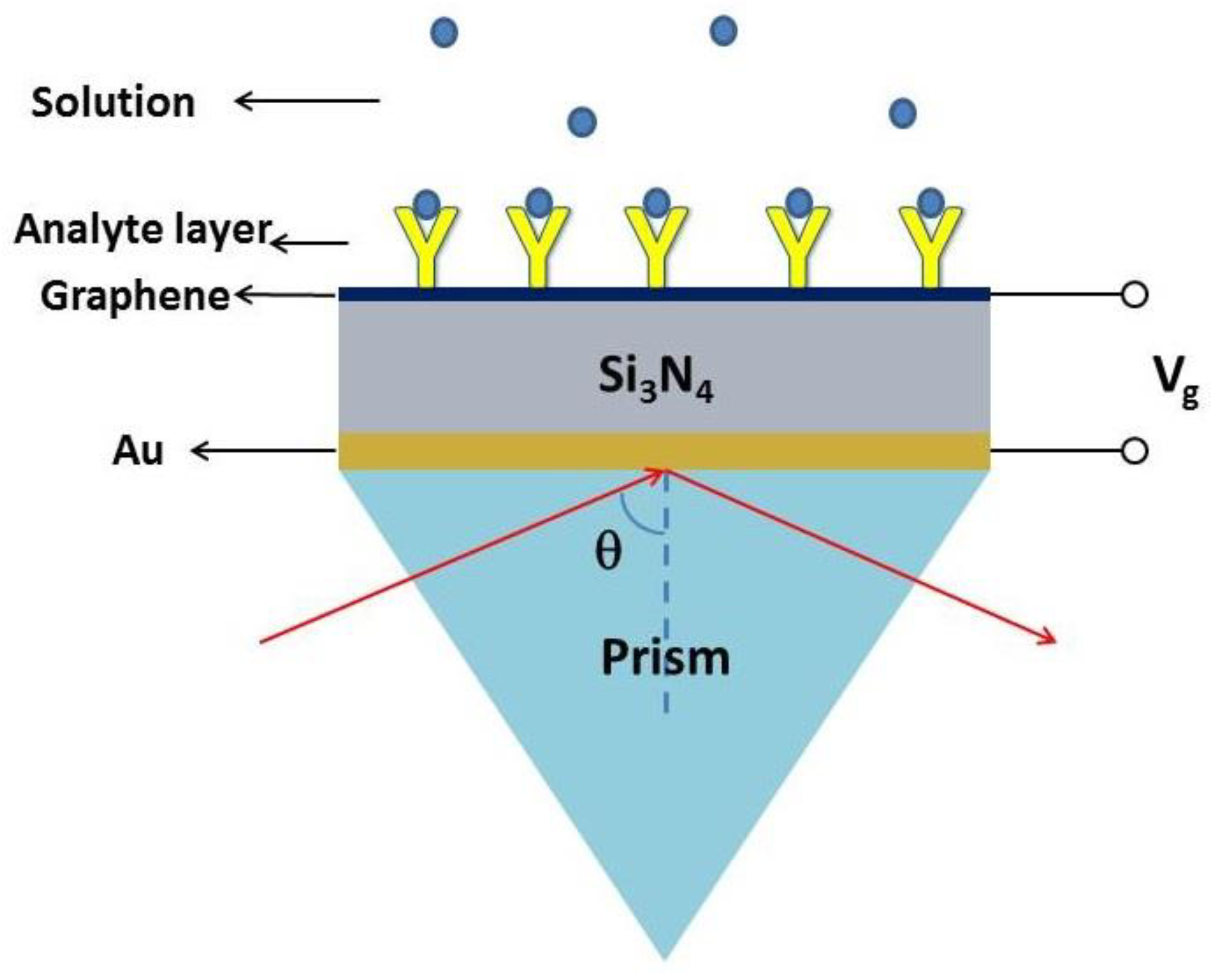
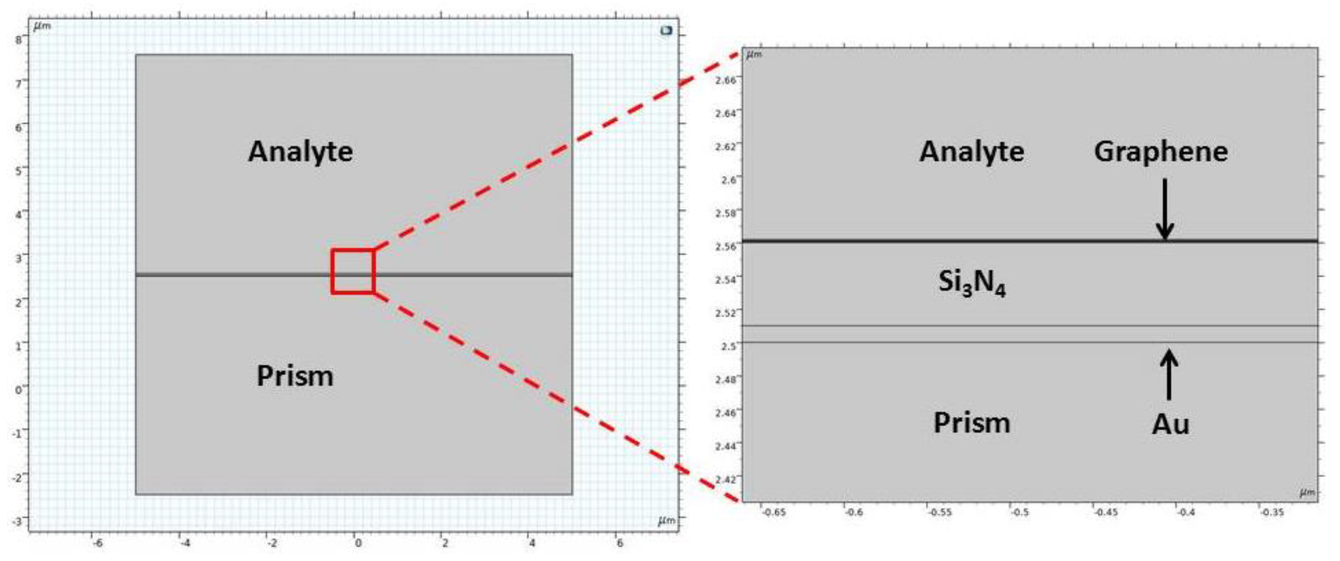
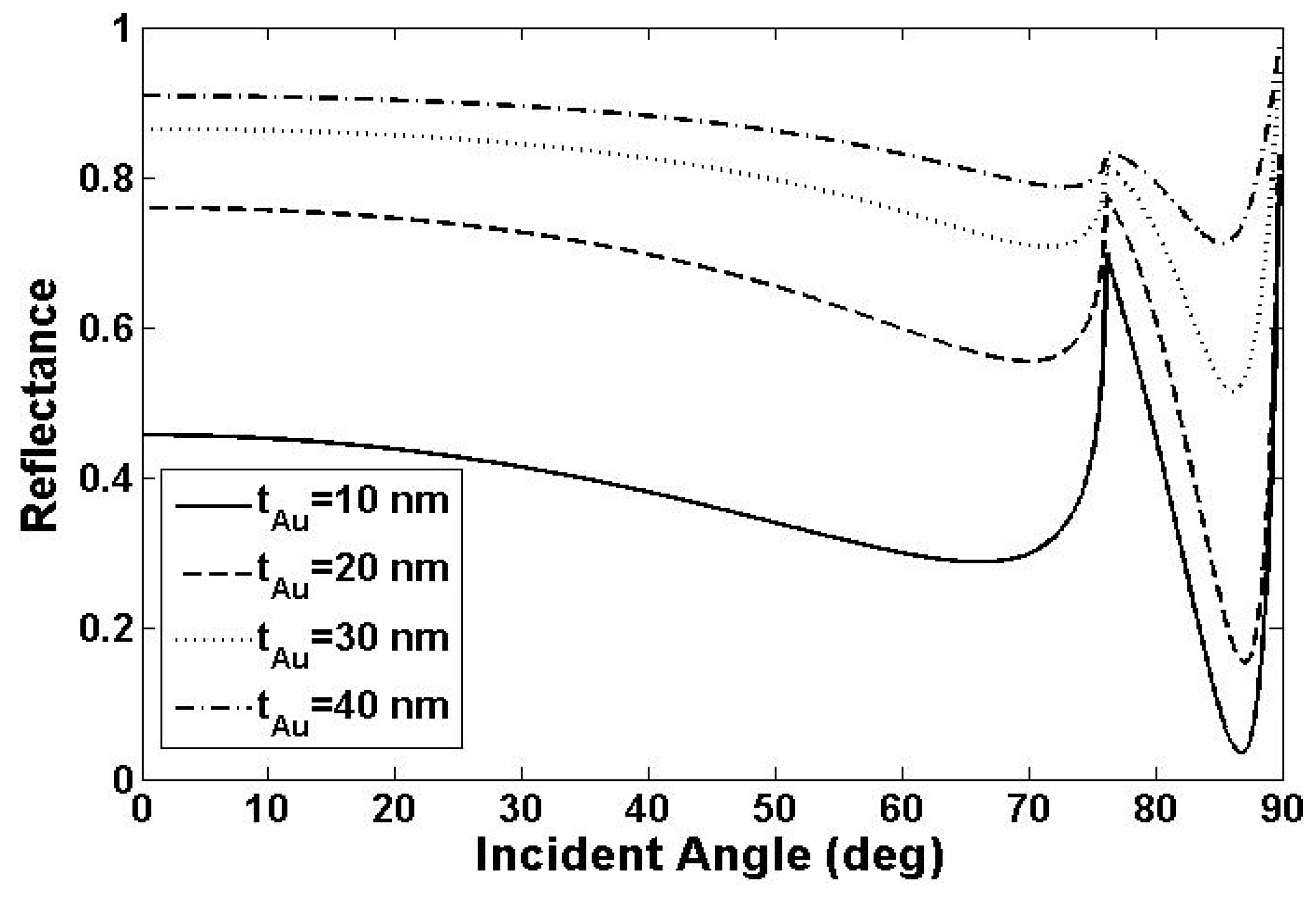
2. Sample Design and Numerical Method
3. Results
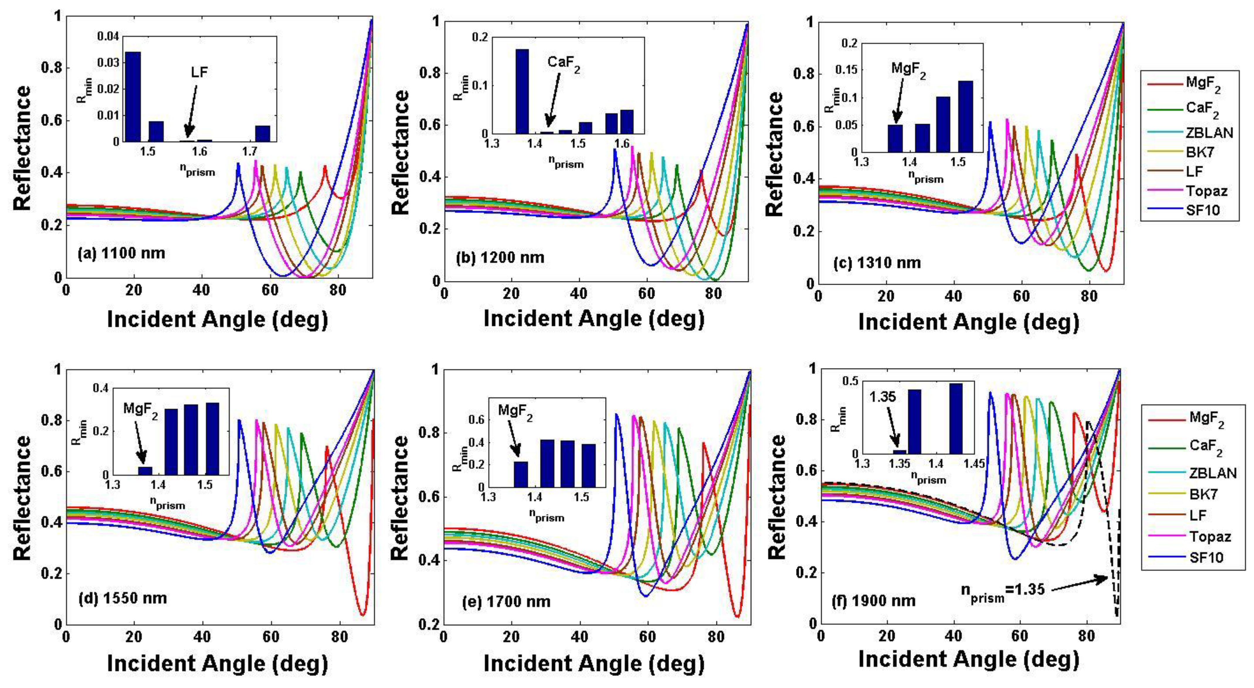
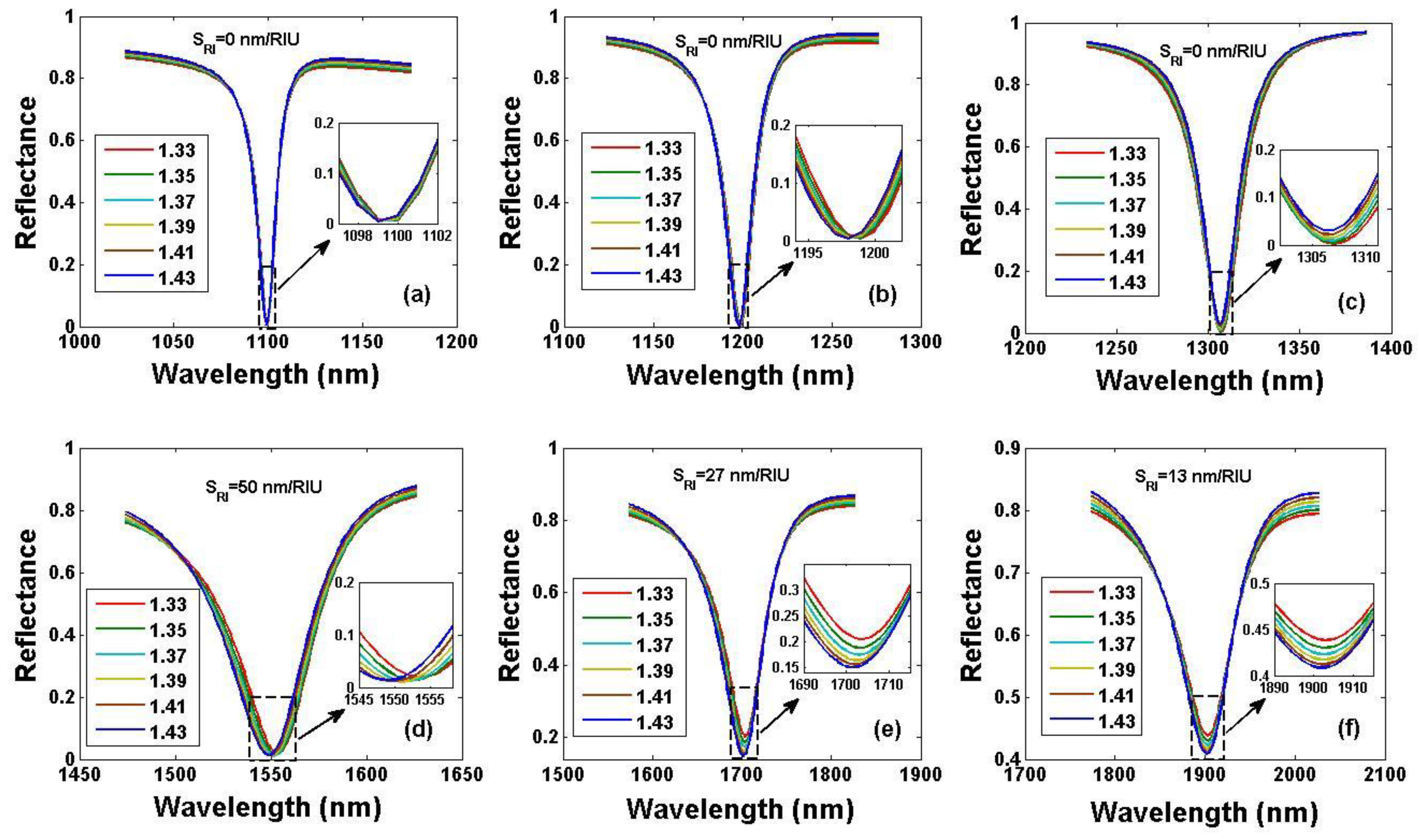
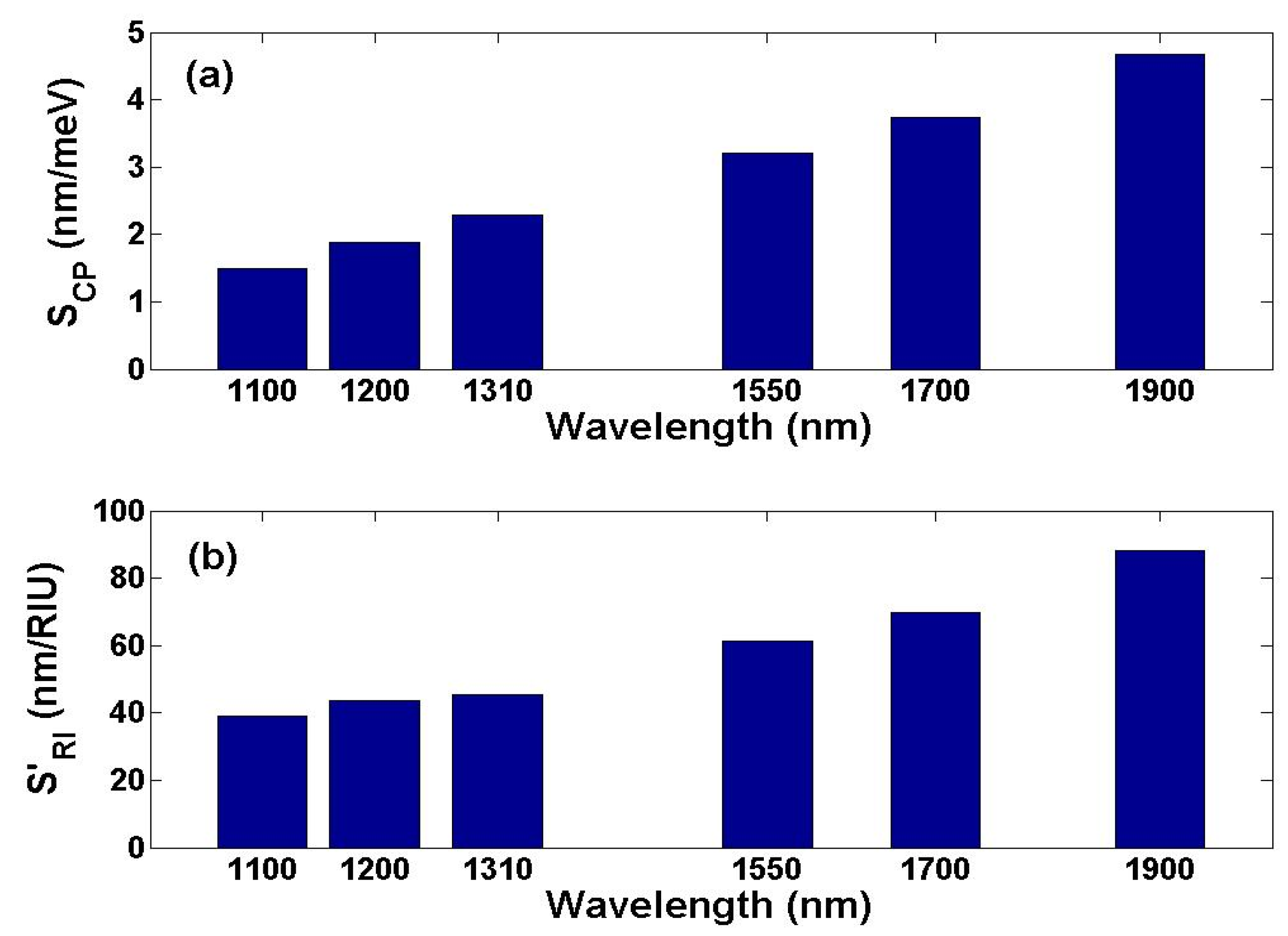
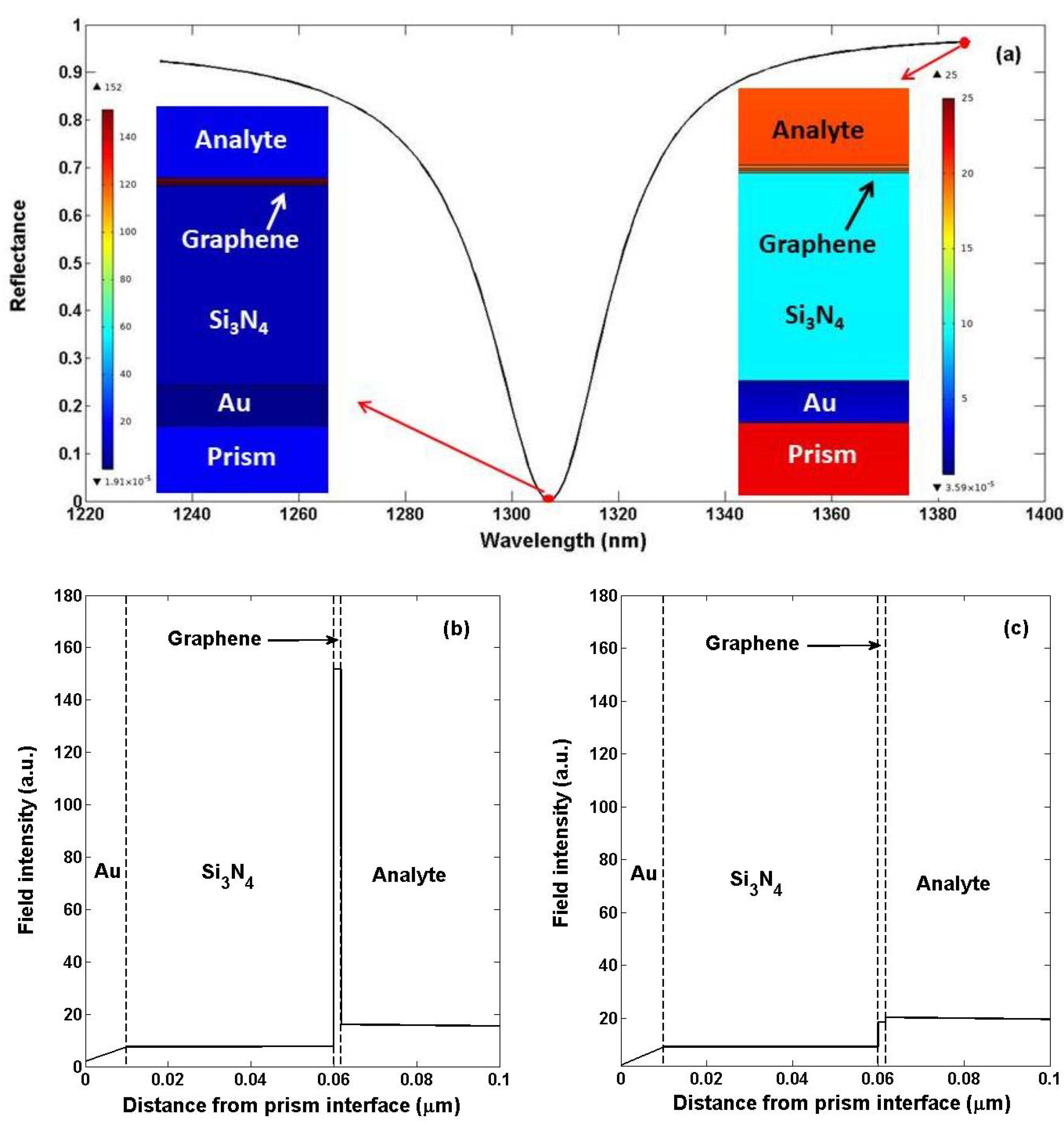
3.1. Sensing Performance Based on Wavelength Interrogation Mode
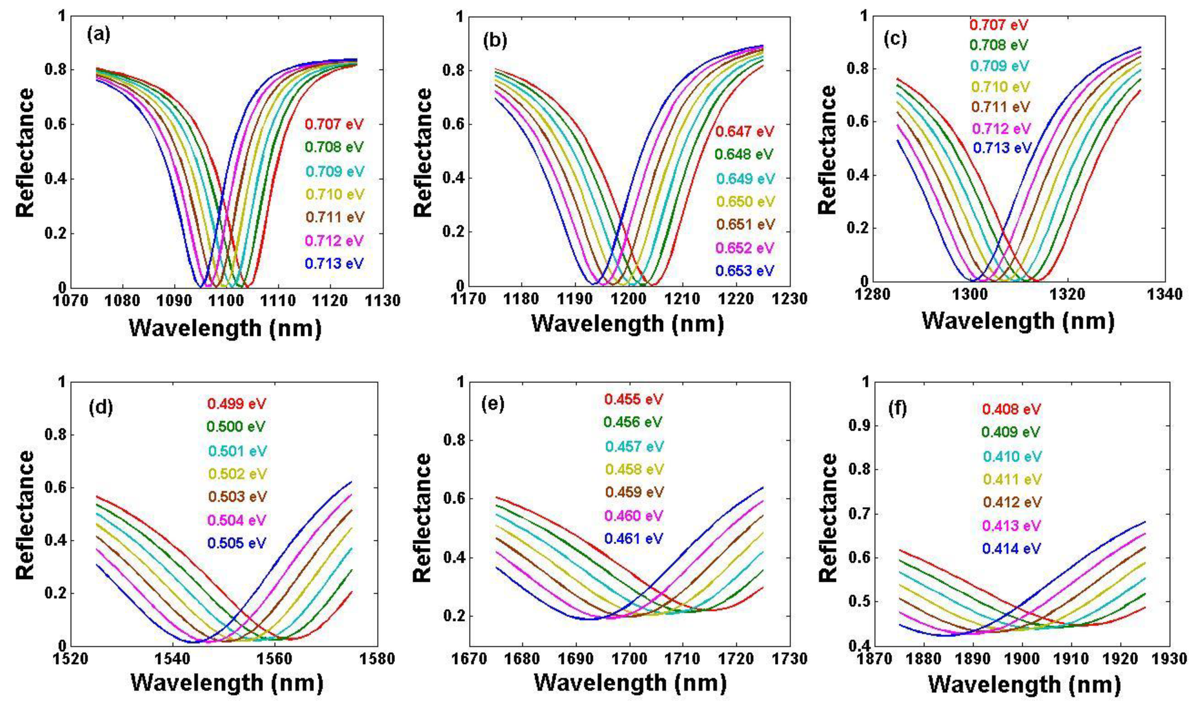
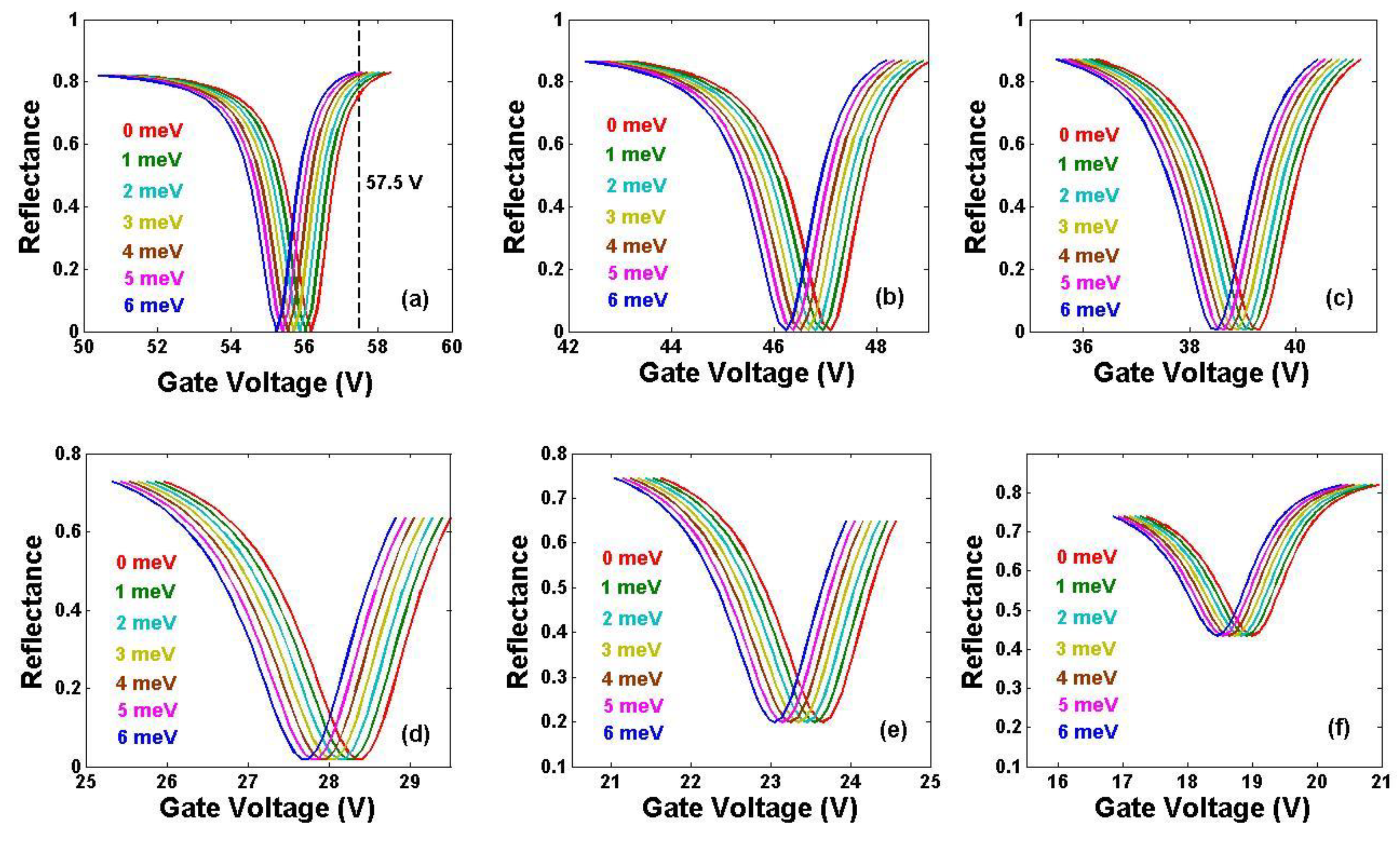
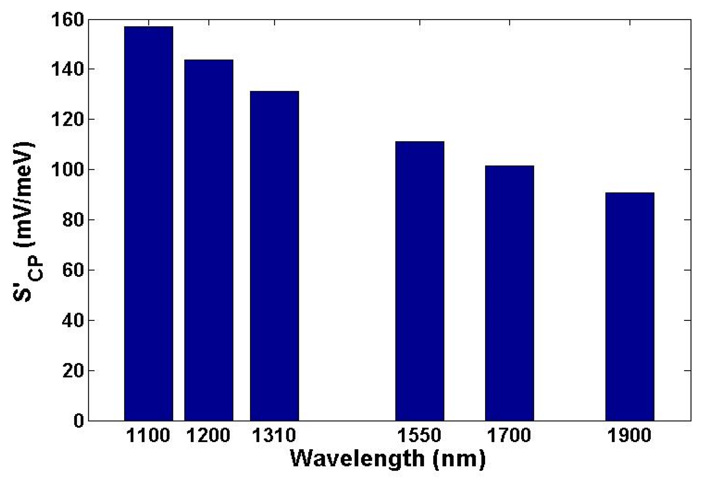
3.2. Sensing Performance Based on Gate Voltage Interrogation Mode
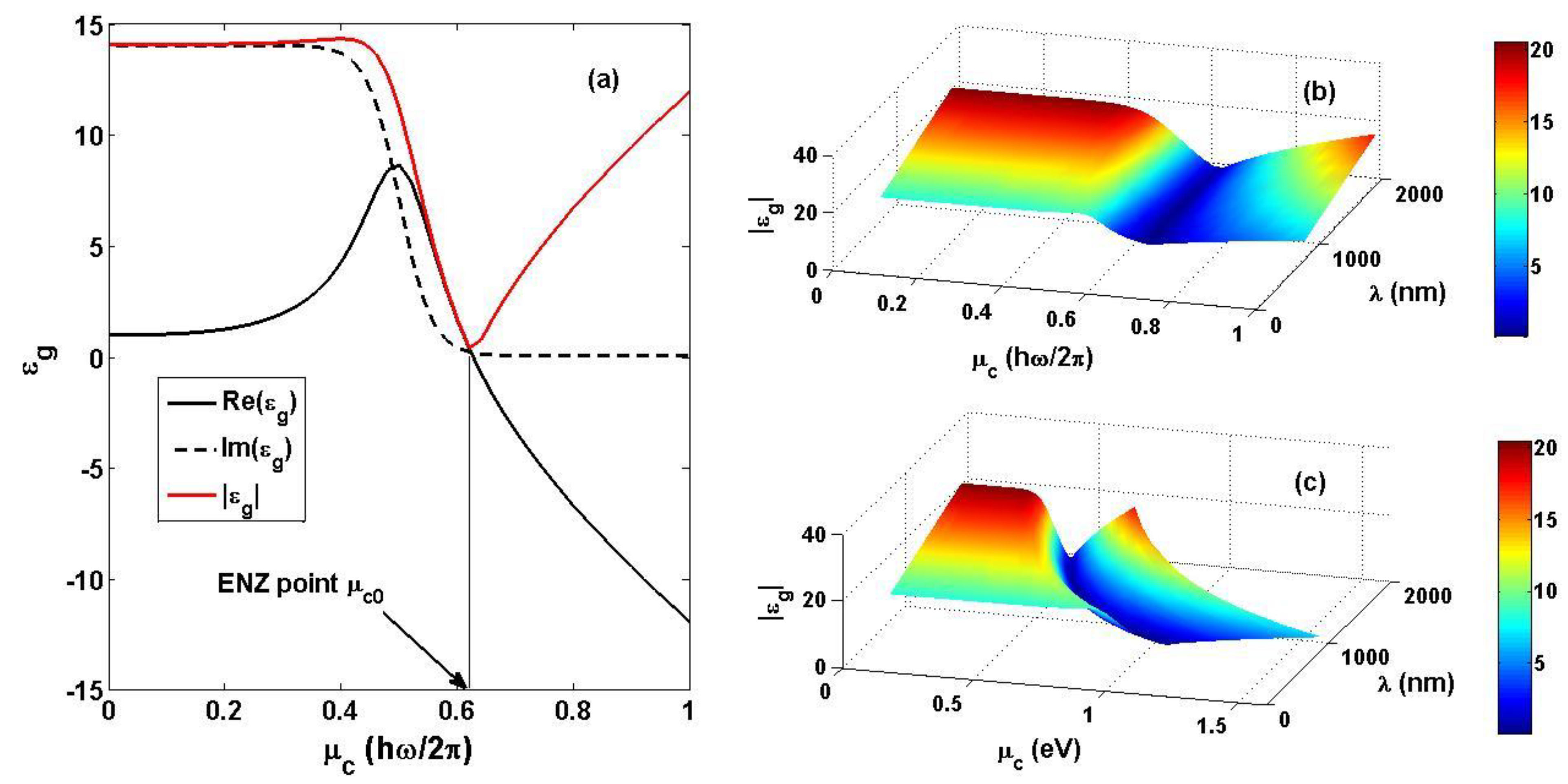
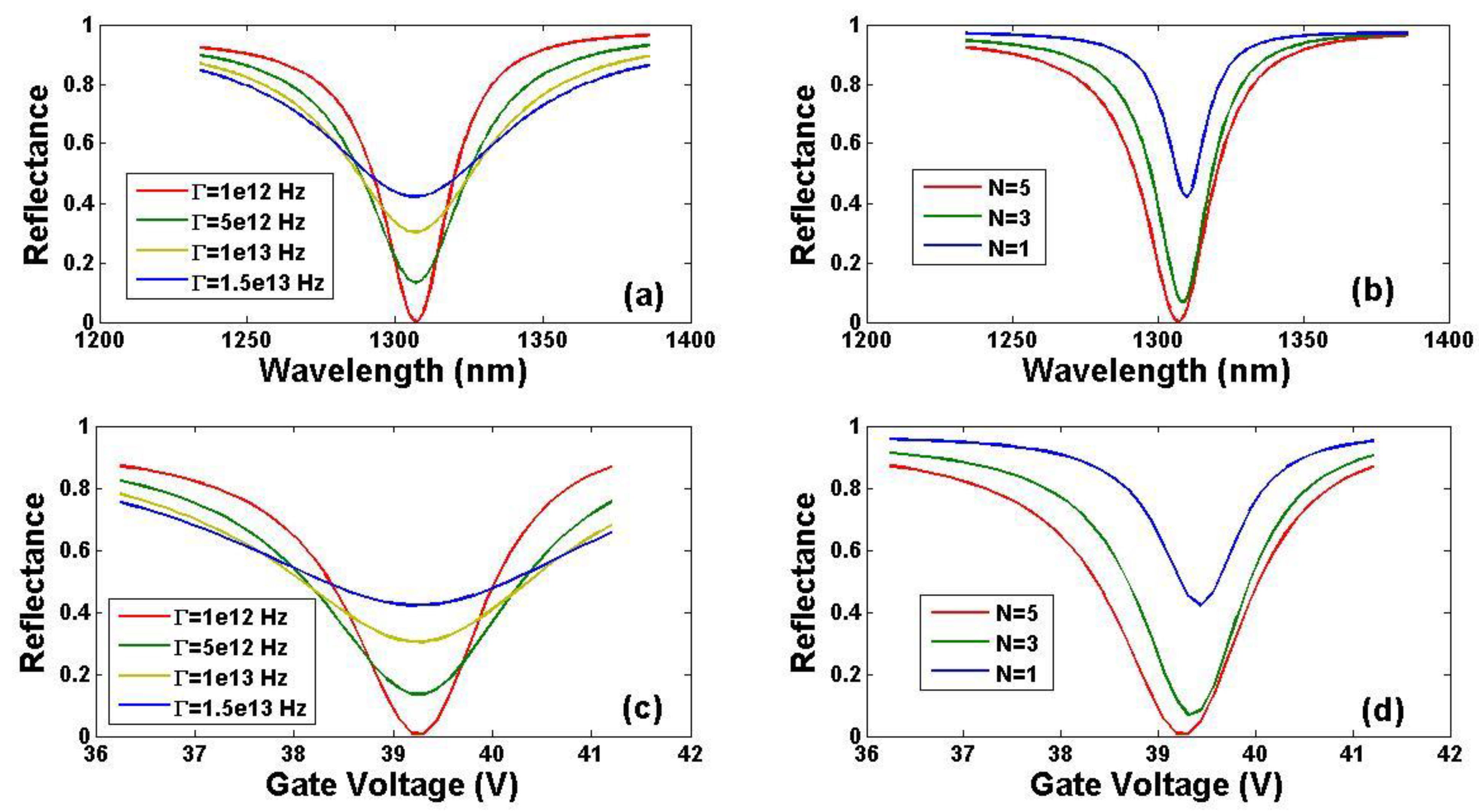
4. Discussion on the Influence of the Quality and the Atom Layer Number of the Graphene Film on the Sensing Performance
5. Conclusions
Author Contributions
Funding
Institutional Review Board Statement
Informed Consent Statement
Data Availability Statement
Conflicts of Interest
Appendix A

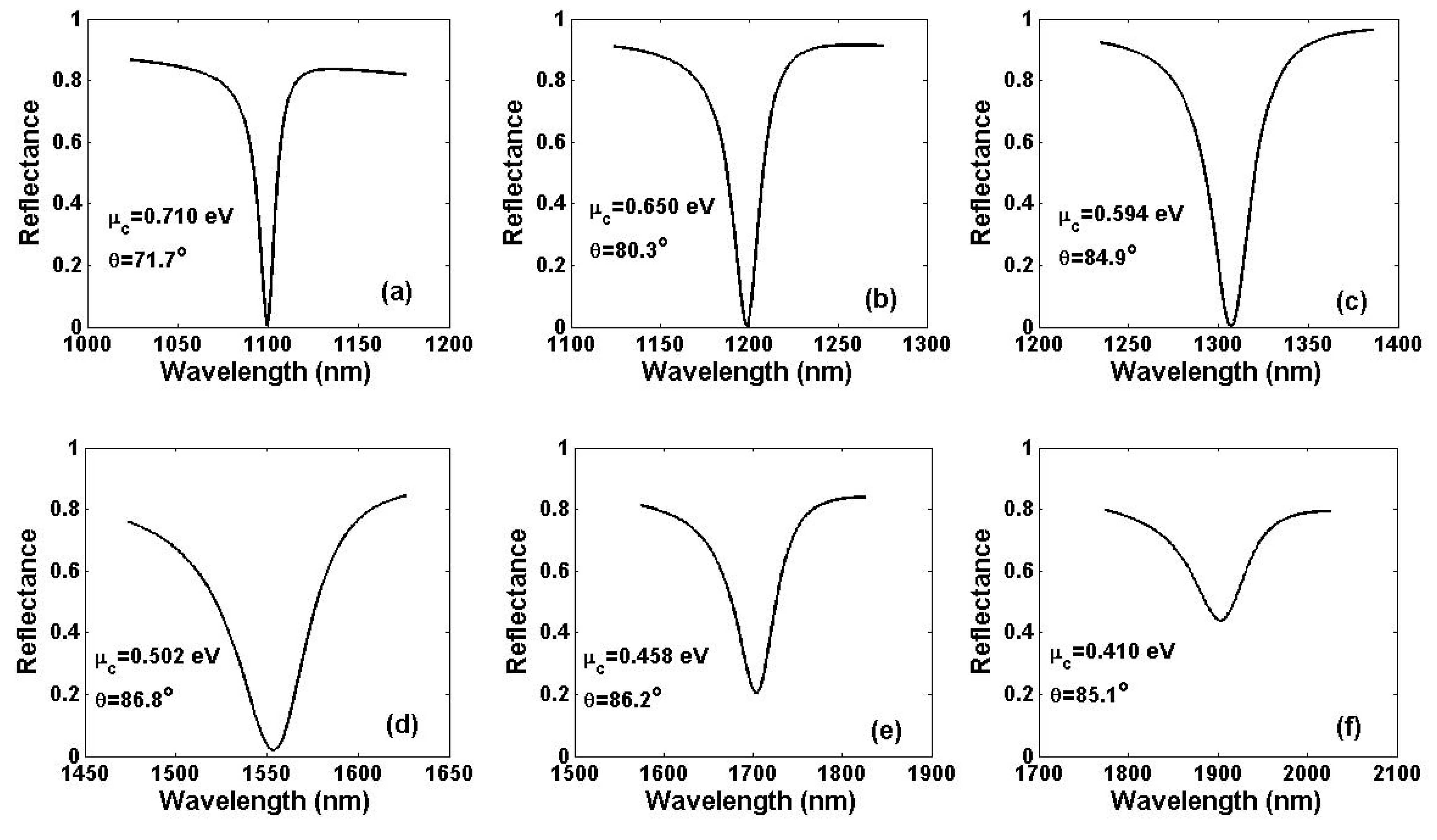
| Si3N4 Layer Thickness | 50 nm | 60 nm | 70 nm | 80 nm | 90 nm | 100 nm | |
|---|---|---|---|---|---|---|---|
| 1100 nm | optimal prism | LF | LF | LF | Topaz | Topaz | Topaz |
| resonance angle | 71.7° | 73.4° | 75.2° | 75.3° | 77.2° | 78.9° | |
| 1200 nm | optimal prism | CaF2 | ZBLAN | ZBLAN | BK7 | BK7 | BK7 |
| resonance angle | 80.3° | 78.9° | 80.7° | 79.7° | 81.6° | 83° | |
| 1310 nm | optimal prism | MgF2 | CaF2 | CaF2 | CaF2 | ZBLAN | ZBLAN |
| resonance angle | 84.9° | 81.8° | 83.7° | 85° | 84.1° | 85.4° | |
| 1550 nm | optimal prism | MgF2 | MgF2 | MgF2 | CaF2 | CaF2 | CaF2 |
| resonance angle | 86.8° | 87.7° | 87.3° | 84.9° | 86.9° | 87.9° | |
| 1700 nm | optimal prism | MgF2 | MgF2 | MgF2 | MgF2 | CaF2 | CaF2 |
| resonance angle | 86.2° | 87.9° | 88.5° | 87.7° | 85.3° | 87.3° | |
| 1900 nm | optimal prism | MgF2 | MgF2 | MgF2 | MgF2 | MgF2 | CaF2 |
| resonance angle | 85.1° | 86.8° | 88.5° | 89° | 88.1° | 85° | |
References
- Homola, J. Present and future of surface plasmon resonance biosensors. Anal. Bioanal. Chem. 2003, 377, 528–539. [Google Scholar] [CrossRef] [PubMed]
- Singh, S.; Singh, P.K.; Umar, A.; Lohia, P.; Albargi, H.; Castaneda, L.; Dwivedi, D.K. 2D nanomaterial-based surface plasmon resonance sensors for biosensing applications. Micromachines 2020, 11, 779. [Google Scholar] [CrossRef] [PubMed]
- He, L.J.; Pagneux, Q.; Larroulet, I.; Serrano, A.Y.; Pesquera, A.; Zurutuza, A.; Mandler, D.; Boukherroub, R.; Szunerits, S. Label-free femtomolar cancer biomarker detection in human serum using graphene-coated surface plasmon resonance chips. Biosens. Bioelectron. 2017, 89, 606–611. [Google Scholar] [CrossRef] [PubMed]
- Xiong, X.; Chen, Y.F.; Wang, H.; Hu, S.Q.; Luo, Y.H.; Dong, J.L.; Zhu, W.G.; Qiu, W.T.; Guan, H.Y.; Lu, H.H.; et al. Plasmonic interface modified with graphene oxide sheets overlayer for sensitivity enhancement. ACS Appl. Mater. Interfaces 2018, 10, 34916–34923. [Google Scholar] [CrossRef]
- Alonso-Murias, M.D.C.; nzon-Hernandez, D.; Gravagnuolo, A.M.; Marquez, S.; Giardina, P.; Morales-Narvaez, E. Graphene oxide biohybrid layer enhances sensitivity and anticorrosive properties in refractive index sensor. J. Phys. Photonics 2021, 3, 034009. [Google Scholar] [CrossRef]
- Yu, H.X.; Chong, Y.; Zhang, P.H.; Ma, J.M.; Li, D.C. A D-shaped fiber SPR sensor with a composite nanostructure of MoS2-graphene for glucose detection. Talanta 2020, 219, 121324. [Google Scholar] [CrossRef]
- Wei, W.; Nong, J.P.; Mei, Y.H.; Zhong, C.Y.; Lan, G.L.; Hu, W.H. Single-layer graphene-coated gold chip for enhanced SPR imaging immunoassay. Sens. Actuators B 2018, 273, 1548–1555. [Google Scholar] [CrossRef]
- Wang, Q.; Wang, X.Z.; Song, H.; Zhao, W.M.; Jing, J.Y. A dual channel self-compensation optical fiber biosensor based on coupling of surface palsmon polariton. Opt. Laser Technol. 2020, 124, 106002. [Google Scholar] [CrossRef]
- Zagorodko, O.; Spadavecchia, J.; Serrano, A.Y.; Larroulet, I.; Pesquera, A.; Zurutuza, A.; Boukherroub, R.; Szunerits, S. Highly sensitive detection of DNA hybridization on commercialized graphene-coated surface plasmon resonance interfaces. Anal. Chem. 2014, 86, 11211–11216. [Google Scholar] [CrossRef]
- Sun, Y.; Cai, H.Y.; Qiao, X.; Wang, X.P. High-performance polarization control modulated surface plasmon resonance sensor based on monolayer graphene/Au-NPs architecture for detection of DNA hybridization. Meas. Sci. Technol. 2019, 30, 125701. [Google Scholar] [CrossRef]
- Xue, T.Y.; Liang, W.Y.; Li, Y.W.; Sun, Y.H.; Xiang, Y.J.; Zhang, Y.P.; Dai, Z.G.; Duo, Y.H.; Wu, L.M.; Qi, K.; et al. Ultrasensitive detection of miRNA with an antimonene-based surface plasmon resonance sensor. Nat. Commun. 2019, 10, 28. [Google Scholar] [CrossRef] [PubMed]
- Chen, S.M.; Liu, C.; Liu, Y.; Liu, Q.; Lu, M.D.; Bi, S.; Jing, Z.G.; Yu, Q.X.; Peng, W. Label-free near-infrared plasmonic sensing technique for DNA detection at ultralow concentrations. Adv. Sci. 2020, 7, 2000763. [Google Scholar] [CrossRef] [PubMed]
- Chen, S.M.; Liu, Y.; Yu, Q.X.; Peng, W. Self-referencing SPR biosensing with an ultralow limit-of-detection using long-wavelength excitation. Sens. Actuators B 2021, 327, 128935. [Google Scholar] [CrossRef]
- Duan, Q.L.; Liu, Y.N.; Chang, S.S.; Chen, H.Y.; Chen, J.H. Surface plasmonic sensors: Sensing mechanism and recent applications. Sensors 2021, 21, 5262. [Google Scholar] [CrossRef] [PubMed]
- Grigorenko, A.N.; Polini, M.; Novoselov, K.S. Graphene plasmons. Nat. Photonics 2012, 6, 749–758. [Google Scholar] [CrossRef]
- Jablan, M.; Soljacic, M.; Buljan, H. Plasmons in graphene: Fundamental properties and potential applications. Proc. IEEE 2013, 101, 1689–1704. [Google Scholar] [CrossRef]
- Ju, L.; Geng, B.S.; Horng, J.; Girit, C.; Martin, M.; Hao, Z.; Bechtel, H.A.; Liang, X.G.; Zettl, A.; Shen, Y.R.; et al. Graphene plasmonics for tunable terahertz metamaterials. Nat. Nanotechnol. 2011, 6, 630–634. [Google Scholar] [CrossRef]
- Yan, H.G.; Li, X.S.; Chandra, B.; Tulevski, G.; Wu, Y.Q.; Freitag, M.; Zhu, W.J.; Avouris, P.; Xia, F.N. Tunable infrared plasmonic devices using graphene/insulator stacks. Nat. Nanotechnol. 2012, 7, 330–334. [Google Scholar] [CrossRef]
- Fang, Z.Y.; Thongrattanasiri, S.; Schlather, A.; Liu, Z.; Ma, L.L.; Wang, Y.M.; Ajayan, P.M.; Nordlander, P.; Halas, N.J.; Abajo, F.J.G.d. Gated tenability and hybridization of localized plasmons in nanostructured graphene. ACS Nano 2013, 7, 2388–2395. [Google Scholar] [CrossRef]
- Brar, V.W.; Jang, M.S.; Sherrott, M.; Lopez, J.J.; Atwater, H.A. Highly confined tunable mid-infrared plasmonics in graphene nanoresonators. Nano Lett. 2013, 13, 2541–2547. [Google Scholar] [CrossRef]
- Fei, Z.; Rodin, A.S.; Andreev, G.O.; Bao, W.; Mcleod, A.S.; Wagner, M.; Zhang, L.M.; Zhao, Z.; Thiemens, M.; Dominguez, G.; et al. Gate-tuning of graphene plasmons revealed by infrared nano-imaging. Nature 2012, 487, 82–85. [Google Scholar] [CrossRef] [PubMed]
- Chen, J.N.; Badioli, M.; Alonso-Gonzalez, P.; Thongrattanasiri, S.; Huth, F.; Osmond, J.; Spasenovic, M.; Centeno, A.; Pesquera, A.; Godignon, P.; et al. Optical nano-imaging of gate-tunable graphene plasmons. Nature 2012, 487, 77–81. [Google Scholar] [CrossRef] [PubMed]
- Garcia de Abajo, F.J. Graphene plasmonics: Challenges and opportunities. ACS Photonics 2014, 1, 135–152. [Google Scholar] [CrossRef]
- Cox, J.D.; Garcia de Abajo, F.J. Nonlinear graphene nanoplasmonics. Acc. Chem. Res. 2019, 52, 2536–2547. [Google Scholar] [CrossRef] [PubMed]
- Wang, Z.L.; Li, T.; Almdal, K.; Mortensen, N.A.; Xiao, S.S.; Ndoni, S. Experimental demonstration of graphene plasmons working close to the near-infrared window. Opt. Lett. 2016, 41, 5345–5348. [Google Scholar] [CrossRef]
- Jiao, L.Y.; Zhang, L.; Wang, X.R.; Diankov, G.; Dai, H.J. Narrow graphene nanoribbons from carbon nanotubes. Nature 2009, 458, 877–880. [Google Scholar] [CrossRef]
- Li, X.L.; Wang, X.R.; Zhang, L.; Lee, S.W.; Dai, H.J. Chemically derived, ultrasmooth graphene nanoribbon semiconductors. Science 2008, 319, 1229–1232. [Google Scholar] [CrossRef]
- Rodrigo, D.; Limaj, O.; Janner, D.; Etezadi, D.; García de Abajo, F.J.; Pruneri, V.; Altug, H. Mid-infrared plasmonic biosensing with graphene. Science 2015, 349, 165–168. [Google Scholar] [CrossRef]
- Iranzo, D.A.; Nanot, S.; Dias, E.J.C.; Epstein, I.; Peng, C.; Efetov, D.K.; Lundeberg, M.B.; Parret, R.; Osmond, J.; Hong, J.Y.; et al. Probing the ultimate plasmon confinement limits with a van der Waals heterostructure. Science 2018, 360, 291–295. [Google Scholar] [CrossRef]
- Yan, H.G.; Li, Z.Q.; Li, X.S.; Zhu, W.J.; Avouris, P.; Xia, F.N. Infrared spectroscopy of tunable dirac terahertz magneto-plasmons in graphene. Nano Lett. 2012, 12, 3766–3771. [Google Scholar] [CrossRef]
- Kumada, N.; Roulleau, P.; Roche, B.; Hashisaka, M.; Hibino, H.; Petkovic, I.; Glattli, D.C. Resonant edge magnetoplasmons and their decay in graphene. Phys. Rev. Lett. 2014, 113, 266601. [Google Scholar] [CrossRef]
- Ni, G.X.; Wang, L.; Goldflam, M.D.; Wagner, M.; Fei, Z.; Mcleod, A.S.; Liu, M.K.; Keilmann, F.; Ozyilmaz, B.; Castro Neto, A.H.; et al. Ultrafast optical switching of infrared plasmon polaritons in high-mobility graphene. Nat. Photonics 2016, 10, 244–248. [Google Scholar] [CrossRef]
- Mikhailov, S.A.; Ziegler, K. New electromagnetic mode in graphene. Phys. Rev. Lett. 2007, 99, 016803. [Google Scholar] [CrossRef]
- Vakil, A.; Engheta, N. Transformation optics using graphene. Science 2011, 332, 1291–1294. [Google Scholar] [CrossRef]
- Hwang, R.B. A theoretical design of evanescent wave biosensors based on gate-controlled graphene surface plasmon resonance. Sci. Rep. 2021, 11, 1999. [Google Scholar] [CrossRef]
- Gao, W.L.; Shu, J.; Qiu, C.Y.; Xu, Q.F. Excitation of plasmonic waves in graphene by guided-mode resonance. ACS Nano 2012, 6, 7806–7813. [Google Scholar] [CrossRef]
- Zhu, X.L.; Yan, W.; Jepsen, P.U.; Hansen, O.; Mortensen, N.A.; Xiao, S.S. Experimental observation of plasmons in a graphene monolayer resting on a two-dimensional subwavelength silicon grating. Appl. Phys. Lett. 2013, 102, 131101. [Google Scholar] [CrossRef]
- Gan, C.H. Analysis of surface plasmon excitation at terahertz frequencies with highly dopted graphene sheets via attenuated total reflection. Appl. Phys. Lett. 2012, 101, 111609. [Google Scholar] [CrossRef]
- Purkayastha, A.; Srivastava, T.; Jha, R. Ultrasensitive THz-plasmonics gaseous sensor using doped graphene. Sens. Actuators B 2016, 227, 291–295. [Google Scholar] [CrossRef]
- Huang, Y.; Zhong, S.C.; Yao, H.Z.; Cui, D.X. Tunable ultrasensitive terahertz sensing based on surface plasmon polariton of doped monolayer graphene. Phys. Status Solidi A 2017, 214, 1600550. [Google Scholar] [CrossRef]
- Huang, Y.; Zhong, S.C.; Shen, Y.C.; Yu, Y.J.; Cui, D.X. Terahertz phase jumps for ultra-sensitive graphene plasmon sensing. Nanoscale 2018, 10, 22466. [Google Scholar] [CrossRef] [PubMed]
- Ziolkowski, R.W. Propagation in and scattering from a matched metamaterial having a zero index of refractive. Phys. Rev. E 2004, 70, 046608. [Google Scholar] [CrossRef] [PubMed]
- Engheta, N. Pursuing near-zero response. Science 2013, 340, 286–287. [Google Scholar] [CrossRef] [PubMed]
- Liberal, I.; Engheta, N. Near-zero refractive index photonics. Nat. Photonics 2017, 11, 149–158. [Google Scholar] [CrossRef]
- Zhu, W.J.; Neumayer, D.; Perebeinos, V.; Avouris, P. Silicon nitride gate dielectrics and band gap engineering in graphene layers. Nano Lett. 2010, 10, 3572–3575. [Google Scholar] [CrossRef] [PubMed]
- Gomez-Diaz, J.S.; Moldovan, C.; Capdevila, S.; Romeu, J.; Bernard, L.S.; Magrez, A.; Lonescu, A.M.; Perruisseau-Carrier, J. Self-biased reconfigurable graphene stacks for terahertz plasmonics. Nat. Commun. 2015, 6, 6334. [Google Scholar] [CrossRef]
- Xiao, Y.; Zhong, Y.C.; Luo, Y.H.; Zhang, J.; Chen, Y.F.; Liu, G.S.; Yu, J.H. Near-infrared tunable surface plasmon resonance sensor based on graphene plasmons via electrostatic gating control. RSC Adv. 2021, 11, 37559–37567. [Google Scholar] [CrossRef] [PubMed]
- Lee, E.J.; Choi, S.Y.; Jeong, H.; Park, N.H.; Yim, W.; Kim, M.H.; Park, J.K.; Son, S.; Bae, S.; Kim, S.J.; et al. Active control of all-fibre graphene devices with electrical gating. Nat. Commun. 2015, 6, 6851. [Google Scholar] [CrossRef]
- Rodrigo, D.; Tittl, A.; Limaj, O.; Abajo, F.J.G.d.; Pruneri, V.; Altug, H. Double-layer graphene for enhanced tunable infrared plasmonics. Light-Sci. Appl. 2017, 6, e16277. [Google Scholar] [CrossRef]
- Mohsin, M.; Neumaier, D.; Schall, D.; Otto, M.; Matheisen, C.; Giesecke, A.L.; Sagade, A.A.; Kurz, H. Experimental verification of electro-refractive phase modulation in graphene. Sci. Rep. 2015, 5, 10967. [Google Scholar] [CrossRef]
- Xiao, Y.; Zhang, J.; Yu, J.H.; Dong, H.Z.; Wei, Y.Y.; Luo, Y.H.; Zhong, Y.C.; Qiu, W.T.; Dong, J.L.; Lu, H.H.; et al. Theoretical investigation of optical modulators based on graphene-coated side-polished fiber. Opt. Express 2018, 26, 13759–13772. [Google Scholar] [CrossRef] [PubMed]
- Meshginqalam, B.; Ahmadi, M.T.; Ismail, R.; Sabatyan, A. Graphene/graphene oxide-based ultrasensitive surface plasmon resonance biosensor. Plasmonics 2017, 12, 1991–1997. [Google Scholar] [CrossRef]
- Gomez-Diaz, J.S.; Esquius-Morote, M.; Perruisseau-Carrier, J. Plane wave excitation-detection of non-resonant plasmons along finite-width graphene strips. Opt. Express 2013, 21, 24856–24872. [Google Scholar] [CrossRef] [PubMed]
- Hanson, G.W. Dyadic Green’s functions and guided surface waves for a surface conductivity model of graphene. J. Appl. Phys. 2008, 103, 064302. [Google Scholar] [CrossRef]
- Luke, K.; Okawachi, Y.; Lamont, M.R.E.; Gaeta, A.L.; Lipson, M. Broadband mid-infrared frequency comb generation in a Si3N4 microresonator. Opt. Lett. 2015, 40, 4823–4826. [Google Scholar] [CrossRef]
- Beliaev, L.Y.; Shkondin, E.; Lavrinenko, A.V.; Takayama, O. Optical, structural and composition properties of silicon nitride films deposited by reactive radio-frequency sputtering, low pressure and plasma-enhanced chemical vapor deposition. Thin Solid Films 2022, 763, 139568. [Google Scholar] [CrossRef]
- Dong, X.C.; Shi, Y.M.; Huang, W.; Chen, P.; Li, L.J. Electrical detection of DNA hybridization with single-base specificity using transistors based on CVD-grown graphene sheets. Adv. Mater. 2010, 22, 1649–1653. [Google Scholar] [CrossRef]
- Mohanty, N.; Berry, V. Graphene-based single-bacterium resolution biodevice and DNA transistor: Interfacing graphene derivatives with nanoscale and microscale biocomponents. Nano Lett. 2008, 8, 4469–4476. [Google Scholar] [CrossRef]
- Sipova, H.; Homola, J. Surface plasmon resonance sensing of nucleic acids: A review. Anal. Chim. Acta 2013, 773, 9–23. [Google Scholar] [CrossRef]
- Artyukhin, A.B.; Stadermann, M.; Friddle, R.W.; Stroeve, P.; Bakajin, O.; Noy, A. Controlled electrostatic gating of carbon nanotube FET devices. Nano Lett. 2006, 6, 2080–2085. [Google Scholar] [CrossRef]
- Song, H.S.; Li, S.L.; Miyazaki, H.; Sato, S.; Hayashi, K.; Yamada, A.; Yokoyama, N.; Tsukagoshi, K. Origin of the relatively low transport mobility of graphene grown through chemical vapor deposition. Sci. Rep. 2012, 2, 337. [Google Scholar] [CrossRef] [PubMed]
- Nguyen, D.T.; Chiang, W.Y.; Su, Y.H.; Hofmann, M.; Hsieh, Y.P. Solid-diffusion-facilitated cleaning of copper foil improves the quality of CVD graphene. Sci. Rep. 2019, 9, 257. [Google Scholar] [CrossRef] [PubMed]
- Shi, H.H.; Guo, Y.X.; Qi, Z.K.; Xie, K.; Zhang, R.X.; Xia, Y.M.; Chen, C.; Zeng, H.L.; Cui, P.; Ji, H.X.; et al. Elimination of grain boundaries in graphene growth on a Cu-Ni alloyed substrate by chemical vapor deposition. J. Phys. Chem. C 2021, 125, 18217–18224. [Google Scholar] [CrossRef]
- Qian, Y.T.; Sohn, M.K.; Park, H.J.; Huang, J.S.; Subramanian, K.R.V.; Kang, D.J. Universal 2D material film transfer using a novel low molecular weight polyvinyl acetate. Appl. Surf. Sci. 2020, 534, 147650. [Google Scholar] [CrossRef]
- Chen, F.; Xia, J.L.; Tao, N.J. Ionic screening of charged-impurity scattering in graphene. Nano Lett. 2009, 9, 1621–1625. [Google Scholar] [CrossRef]
- Romagnoli, M.; Sorianello, V.; Midrio, M.; Koppens, F.H.L.; Huyghebaert, C.; Neumaier, D.; Galli, P.; Templ, W.; D’Errico, A.; Ferrari, C. Graphene-based integrated photonics for next-generation datacom and telecom. Nat. Rev. Mater. 2018, 3, 392–414. [Google Scholar] [CrossRef]
- Huang, M.; Bakharev, P.V.; Wang, Z.J.; Biswal, M.; Yang, Z.; Jin, S.W.; Wang, B.; Park, H.J.; Li, Y.Q.; Qu, D.S.; et al. Large-area single-crystal AB-bilayer and ABA-trilayer graphene grown on a Cu/Ni(111) foil. Nat. Nanotechnol. 2020, 15, 289–295. [Google Scholar] [CrossRef]


| Λ (nm) | 760 | 850 | 980 | 1100 | 1200 | 1310 | 1550 | 1700 | 1900 |
|---|---|---|---|---|---|---|---|---|---|
| μc0 (eV) | 1.037 | 0.923 | 0.798 | 0.709 | 0.649 | 0.594 | 0.502 | 0.458 | 0.410 |
| μcPR (eV) | 1.037 | 0.923 | 0.798 | 0.710 | 0.650 | 0.594 | 0.502 | 0.458 | 0.410 |
| Vg (V) | 119.6 | 94.8 | 70.9 | 56.2 | 47.1 | 39.4 | 28.2 | 23.5 | 18.9 |
| SPR Structure | Theoretical/Experimental | LOD | FWHM | Ref. |
|---|---|---|---|---|
| HBAK1/Au film/graphene/AuNSs | experimental | 0.5 fM | - | [9] |
| K9/Au film/graphene/AuNPs | experimental | 0.5 fM | - | [10] |
| K9/Au film/antimonene/AuNRs | experimental | 10 aM | - | [11] |
| K9/AuNT array/AuNPs | experimental | 1.2 aM | 114.471 nm | [12] |
| K9/Au film/GO-AuNPs | experimental | 0.2 fM | - | [13] |
| MgF2/Au film/Si3N4/graphene | theoretical | <4.27 fM | 78.4 nm | this work |
| LF/Au film/Si3N4/graphene | theoretical | <21.66 aM | 1158 mV | this work |
Disclaimer/Publisher’s Note: The statements, opinions and data contained in all publications are solely those of the individual author(s) and contributor(s) and not of MDPI and/or the editor(s). MDPI and/or the editor(s) disclaim responsibility for any injury to people or property resulting from any ideas, methods, instructions or products referred to in the content. |
© 2023 by the authors. Licensee MDPI, Basel, Switzerland. This article is an open access article distributed under the terms and conditions of the Creative Commons Attribution (CC BY) license (https://creativecommons.org/licenses/by/4.0/).
Share and Cite
Xiao, Y.; Cui, D.; Zhong, Y.; Li, Z.; Zhang, J.; Yu, J. Theoretical Design of Near-Infrared Tunable Surface Plasmon Resonance Biosensors Based on Gate-Controlled Graphene Plasmons. Coatings 2024, 14, 56. https://doi.org/10.3390/coatings14010056
Xiao Y, Cui D, Zhong Y, Li Z, Zhang J, Yu J. Theoretical Design of Near-Infrared Tunable Surface Plasmon Resonance Biosensors Based on Gate-Controlled Graphene Plasmons. Coatings. 2024; 14(1):56. https://doi.org/10.3390/coatings14010056
Chicago/Turabian StyleXiao, Yi, Danting Cui, Yongchun Zhong, Zhibin Li, Jun Zhang, and Jianhui Yu. 2024. "Theoretical Design of Near-Infrared Tunable Surface Plasmon Resonance Biosensors Based on Gate-Controlled Graphene Plasmons" Coatings 14, no. 1: 56. https://doi.org/10.3390/coatings14010056