
High-Power Impulse Magnetron Sputter-Deposited Chromium-Based Coatings for Corrosion Protection

1
Department of Materials Science and Engineering, Feng Chia University, No. 100, Wenhwa Rd., Seatwen District, Taichung 40724, Taiwan
2
Center for Low-Temperature Plasma Sciences, Nagoya University, Furocho, Chikusaku, Nagoya 464-0863, Japan
3
Institute of Plasma, Feng Chia University, No. 100, Wenhwa Road, Seatwen District, Taichung 407102, Taiwan
*
Author to whom correspondence should be addressed.
Coatings 2023, 13(12), 2101; https://doi.org/10.3390/coatings13122101
Submission received: 13 November 2023
/
Revised: 10 December 2023
/
Accepted: 14 December 2023
/
Published: 18 December 2023
(This article belongs to the Special Issue Application of Advanced Plasma Technology in Coatings, Films and Etching)
Abstract
:The use of high-power impulse magnetron sputtering (HIPIMS) to deposit chromium-based thin films on brass substrates for the purpose of corrosion-protective coating was investigated. By varying the process parameters (pulse frequency, pulse width and N2 flow rate) and structure design, including single-layer and multilayer structures, the obtained results revealed that the Cr-N films deposited through the use of HIPIMS exhibited higher film density and corrosion resistance compared to traditional direct-current magnetron sputtering. Based on the results of a field test using copper-accelerated acetic acid solution, the Cr-N film with a multilayered structure can further extend the time to corrosion onset. This is because the bottom layer in the multilayer structure can block structural defects in the layer above it, effectively reducing the penetration of corrosive agents into the substrate. The high bias voltage, coupled with increased temperature during deposition, led to a dezincification effect, resulting in the reduced adhesion of the film to the substrate and decreased overall corrosion resistance.
1. Introduction
As is well known, electroplating stands out as one of the most crucial surface treatment processes in today’s industrial landscape. However, in the context of addressing the environmental concerns associated with this process, every nation grapples with significant operational expenses incurred in managing the disposal of wastewater and the emissions generated during electroplating. In 2003, the European Union (EU) enacted the Restriction of Hazardous Substances (RoHS) directive, which was enforced and became effective in July 2006. This directive was instituted to proscribe the utilization of specific substances, such as lead, mercury, Cr6+, and others, in diverse processes, equipment, and materials [1,2]. The EU not only initiated the development of these specifications but also prompted the United States, Japan and several other nations to establish relevant laws and regulations concerning environmentally sustainable products. The Chinese government’s decision in 2017 to halt numerous electroplating lines garnered considerable attention, highlighting China’s dedication to environmental protection.
Physical vapor deposition (PVD) processes have long been regarded as viable alternatives to traditional electroplating methods. These PVD processes offer a broad range of coating materials suitable for both decorative and protective purposes. This consideration has led to these processes being explored as alternative methods to replace electroplating coatings for applications related to both decorative and corrosion protection. Ceramic coatings, which consist of transition metal nitrides like TiN, TiAl, CrN, and NbN, have found extensive use in industrial applications [3]. This is primarily due to their ability to offer wear protection, heat and corrosion resistance, strong adhesion, and high levels of hardness. When taking into account both corrosion resistance and color appearance, chromium nitride (CrN) coatings emerged as the optimal choice for this research project. CrN coatings exhibit outstanding qualities as hard films and have been widely employed in various industrial applications to safeguard base materials against wear [4], corrosion [5,6,7] and various other surface-related damage issues. As an example, CrN coatings have replaced TiN coatings in numerous applications. This transition is primarily attributed to their similar mechanical properties, with the added advantage of CrN exhibiting superior oxidation resistance at elevated temperatures. Furthermore, the deposition rates for CrN can be as much as three times higher compared to those of TiN [8]. Previous studies have demonstrated that CrN exhibits a high density, which translates into superior corrosion resistance compared to galvanic layers. This characteristic makes CrN a preferred selection for this study, particularly in the context of substituting conventional chromium plating, predominantly owing to its outstanding corrosion resistance [9]. Nevertheless, progress in this regard has been constrained, which is primarily attributed to the corrosion challenges presented by defects, such as through thickness holes and voids, which are inherent in the coating as a result of conventional PVD film structures [10,11,12,13]. Significant challenges still remain, and it is imperative to invest efforts in leveraging advanced PVD techniques to achieve a comprehensive PVD coating layer structure that not only meets the requirements in terms of corrosion resistance but also fulfills decorative purposes.
High-power impulse magnetron sputtering (HIPIMS) has emerged and has been increasingly applied in various industries in recent years. This innovative technique is capable of generating dense and exceptionally well-adhered coatings, essential for fulfilling the requirements of both corrosion protection and decorative layers due to its elevated ionization degree, high plasma density, and substantial ion energy [14,15,16]. Numerous studies have sought to deposit CrN films using HIPIMS. Guimaraes et al. investigated the microstructure of CrN coatings grown by DCMS and HIPIMS with various bias voltages [10]. The continuous growth of a columnar structure, causing a decrease in coating density, is typically an undesired feature for applications requiring corrosive resistance. Therefore, the fine-grained, dense and compact microstructure provided by HIPIMS is generally beneficial for enhancing corrosion resistance [17,18]. Li et al. conducted a correlation study involving optical emission spectroscopic analysis and examined the crystal structure and mechanical properties of the CrN films using HIPIMS and DCMS [19]. The research revealed a lower corrosion current under NaCl solution attributed to the compact structure of the coatings deposited using HIPIMS. In another study by Zhang et al., CrN coatings were deposited on ABS substrates, and the electrochemical corrosion resistance between HIPIMS and DCMS was also compared [20]. The findings indicated that CrN coatings prepared through the use of HIPIMS exhibited superior corrosion current and voltage under NaCl solution. Additionally, Zhu et al. prepared a multilayer Cr/CrN coating using arc evaporation and hybrid HIPIMS, and they compared the microstructure and corrosion resistance of the films [21]. The majority of studies focusing on the corrosion resistance of the coatings rely on potentiodynamic polarization tests. Although the potentiodynamic polarization curve is a valuable method for rapidly accessing the corrosion resistance of coatings due to its quick and convenient nature, practical applications demand long-term duration field tests. Standard methods such as exposure to acetic acid solution or copper-accelerated acetic acid salt solution (CASS) are essential for evaluating corrosion protection performance, particularly for decorative coatings.
In this study, HIPIMS is utilized to deposit both single-layer and multilayer chromium-based coatings on copper alloy substrates. This paper provides a brief overview of the corrosion resistance of the resulting HIPIMS Cr-N coatings with single-layer and multilayer structures. The corrosive resistance of the coatings was analyzed through electrochemical methods and, more importantly, a long-term field test using the CASS method. Furthermore, the microstructures of these coatings were examined to establish a correlation with their respective effectiveness in terms of providing corrosion protection. The findings reveal that the multilayer-structured samples managed to withstand the test for a full 8 h, demonstrating extended corrosion protection. However, the multilayer coatings with a HIPIMS Cr seed layer prepared at high substrate bias displayed reduced corrosion protection.
2. Experimental Section
2.1. Coatings Deposition
The chromium nitride coatings were deposited onto Cu0.64Zn0.36 brass substrates through the use of HIPIMS utilizing pure metallic Cr targets. A comparative analysis was conducted with traditional electroplating and Cr-N single-layer samples prepared through the direct-current magnetron sputtering (DCMS) method. Prior to the coating processes, the substrates underwent ultrasonic cleaning, were air-dried, and were subsequently positioned within the vacuum chamber. The target-to-substrate distance was consistently maintained at 11.5 cm for all coated samples. Once the vacuum chamber was fully evacuated, argon was introduced to initiate argon ion bombardment etching. The deposition process involved applying single-layer and multilayer coating, which were derived from a pure chromium target (99.9%) within an argon and nitrogen atmosphere. This was completed while carefully controlling various parameters to achieve the desired film microstructure. In HIPIMS operation, there is essentially a trade-off between the ionized flux fraction of the sputtered material and a high deposition rate [22,23]. A high ionization flux fraction, coupled with a high peak current to the sputtered target, typically lead to the formation of fine-grained, well-structured, and dense coatings. However, this comes at the expense of a low deposition rate, which also means lower productivity. In preliminary experiments, we optimized deposition parameters such as pulse frequency, duty ratio, pulse width, deposition power, etc., and also observed peak current number of arcing, and deposition rate. The deposition conditions, each defined by a specific set of deposition parameters, along with their corresponding sample names, are detailed in Table 1, Table 2, Table 3 and Table 4 and Figure 1 for both single-layer and multilayer structures (also see Supplementary Materials File). The corrosion resistance of the coatings during CASS field tests was influenced not only by the nature of corrosion resistance but also by the thickness of the coatings. Consequently, the deposition time is primarily determined by the deposition rates of coatings. To achieve a thickness of approximately 3 μm (roughly 30% of the total thickness of the electroplating sample), we adjusted the deposition time. Given that the deposition rate for CrN coatings using HIPIMS is slower than DCMS and conventional electroplating, we extended the deposition time from 15 to 30 min solely for the multilayer series to increase the total thickness of the multilayer. The parameter setups and variations vs. process time can be found in the Supplementary Materials in detail.
2.2. Coating Characterization
The cross-section microstructure and composition of the coating were examined using cold-field emission scanning electron microscopy (FESEM, S-4800, HITACHI, Japan) with an energy-dispersive spectrometer (Oxford, Abingdon, UK). The crystallographic characteristics of the films were analyzed using X-ray diffractometry (XRD, D2 Bruker, Billerica, MA, USA) with Cu Kα radiation. The electrochemical corrosion behavior was assessed using the DC polarization method. The experiments were conducted with the Bio-Logic 150 potentiostat, employing the three-electrode technique. In this step, a platinum electrode was employed as the counter electrode, while the Ag/AgCl electrode served as a reference electrode to measure the potential. The electrochemical investigations were conducted in a test solution known as the CASS, as per the specifications outlined in ASTM B368-09 [24]. The potential range was varied from −0.3 V to 0.6 V, with a scan rate of 0.5 mV/s, and the exposed area was set at 1 cm2. To access the corrosion protection function of the Cr-N coatings, a comprehensive salt spray test was carried out in accordance with the standard method defined in ASTM B368-09 [13]. Both the bare substrate and all coated samples were positioned inside a salt spray chamber (KAUGE Ltd. ST-BS-N, Taichung, Taiwan). The fogging within the chamber was generated using CASS solution, and the temperature was maintained at 49 ± 1 °C. The test samples were periodically removed at fixed intervals (every 4 h) for observation and recording, with the entire test duration spanning 8 h.
3. Results and Discussion
3.1. HIPIMS Waveforms
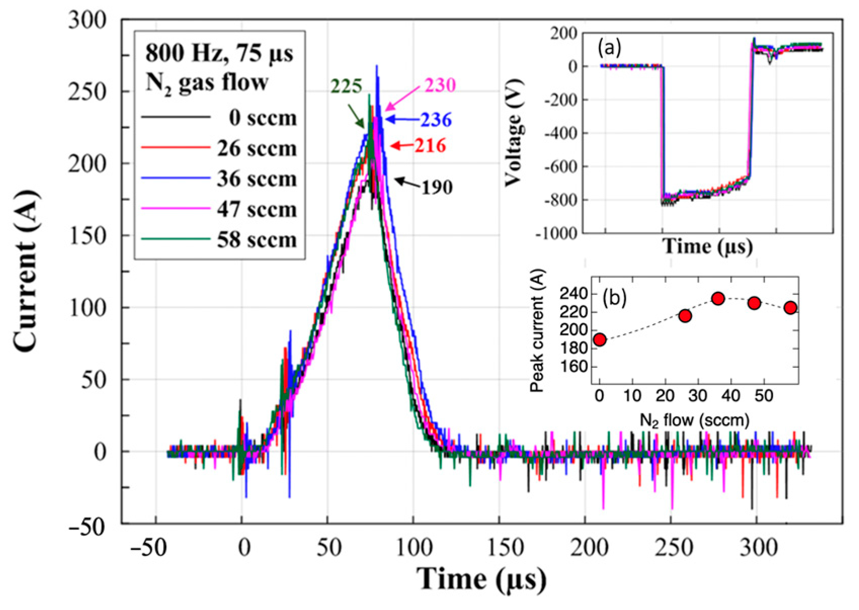
Figure 2 displays the typical current and voltage waveforms recorded during the HIPIMS discharge. The pulse conditions were fixed at a duration of 75 μs, a frequency of 800 Hz, and an average output power of 6 kW. In all experiments, the working pressure was consistently maintained at 1.5 mTorr, and the controlled increase in N2 flow ranged from 0 to 58 sccm. When operating in the metallic mode, the peak discharge current reached 190 A, as illustrated in the inset (b) of Figure 2. Notably, as the N2 flow increased from 0 to 36 sccm, the peak discharge current gradually rose to 236 A. This observed increase indicates a transition from metallic sputtering mode to the nitride mode. With the increase in N2 partial pressure, nitride compounds began to accumulate on the Cr target, leading to a slight target poisoning effect, subsequently causing a reduction in peak current [25,26]. Target poisoning occurs when a compound layer forms on the target due to reactive ion sputtering. Since the bonding energy of compounds is generally much greater than that of metal counterparts, one can expect that the sputter yield always increases when poisoning occurs. In other words, a lower deposition rate can also be anticipated. Therefore, carefully controlling just enough reactive gas to obtain a compound film with sufficient physical properties while maintaining a metallic state of the target surface is crucial.
3.2. Chemical Composition and Crystal Structure
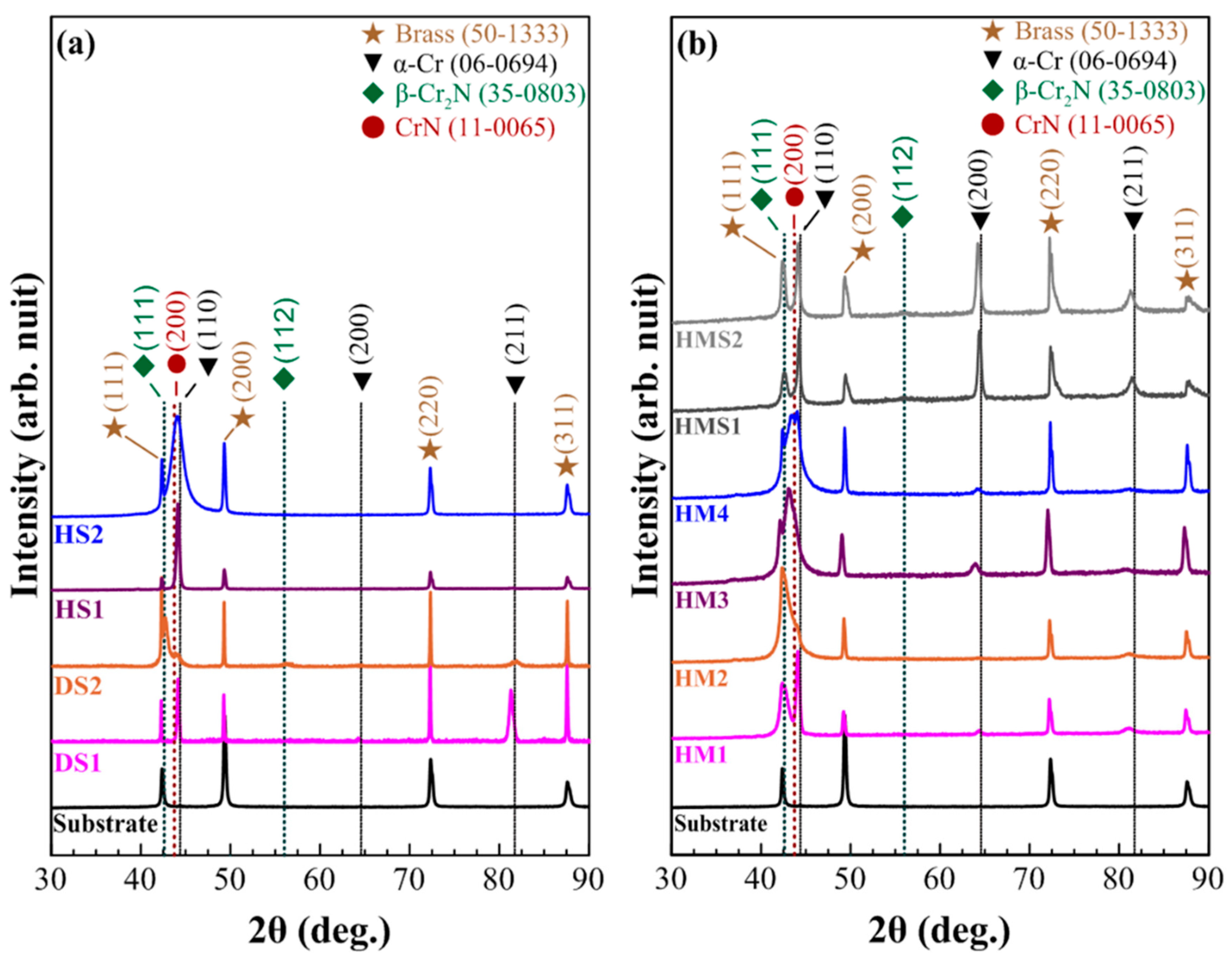
Cr-N coatings, when deposited through reactive magnetron sputtering, typically comprise a combination of Cr, Cr(N), Cr(N) + Cr2N, Cr2N + CrN, and CrN, with the specific composition varying according to the N2 partial pressure [27,28,29,30]. The crystallographic structures of the as-deposited coatings are illustrated in Figure 3. In Figure 3a, the DS1 sample of DCMS Cr coatings exhibited body center cubic (bcc) Cr (110) and (211) peaks. In contrast, the HS1 sample prepared using HIPIMS prominently exhibited a strong (110) peak, suggesting distinct grain growth kinetics compared to the DS1 sample. Furthermore, in the case of CrN coatings for DS2 and HS2 samples, the addition of N2 resulted in a mixture of α-Cr(N) and β-Cr2N phases. This phase mixture led to the emergence of a broad and relatively weak diffraction peak that closely resembled the standard Cr2N (111) peak. As depicted in Figure 3b, the HM1 Cr-N multilayer sample exhibited two distinct structures. This is evident from the presence of Cr (110) and Cr2N (111) peaks, which correspond to the alternating changes in the N2 flow rate.
For the other coatings in the HM series, a comparable evolution of crystal phases was observed. This transition extended from Cr(N) to β-Cr2N, then to a combination of β- Cr2N and c-CrN, and ultimately to pure c-CrN, correlating with an increase in the N2 concentration. In the multilayer design of the HMS1 and HMS2 samples, a resemblance to the HM1 sample is observed, with the presence of crystal structures such as Cr (110) and Cr2N (111). Additionally, the diffraction peaks for Cr (200) and (211) are more pronounced, primarily attributed to the underlying Cr-seeding layer, which results in improved crystallinity.
3.3. Microstructural Characterization
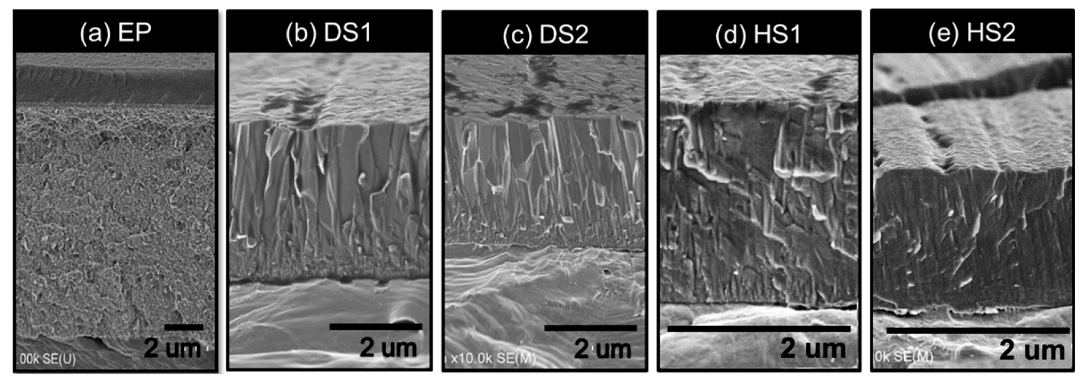
The SEM images illustrating the cross-sectional microstructure of the electroplated and PVD single-layer coatings are displayed in Figure 4. In Figure 4a, the electroplated sample featured a structure with traditional Cr/Ni/Cu forming the anti-corrosion bottom layer and a traditional PVD decorative Cr top layer. The bottom layer displayed a porous microstructure, whereas the top layer exhibited greater density. The combined thickness of these layers resulted in an overall thickness of 10 μm. The single-layer coating prepared via DCMS was characterized by a coarse and open columnar structure, as illustrated in the SEM morphology images shown in Figure 4b,c. In contrast, the HIPIMS single-layer samples, as shown in Figure 4d,e, exhibited a dense and fine structure. Furthermore, the SEM observations on HIPIMS coatings also reveal that the thickness of CrN coatings (Figure 4d and Table 5) was thinner than that of the Cr coatings (Figure 4e and Table 5), which is likely attributed to the lower sputtering yield of N2 gas compared to Ar, which is consistent with the findings in the literature [31]. Due to the re-sputtering effect and other factors [10,22], the deposition rate using DCMS is typically several times that using HIPIMS (see Table 5).
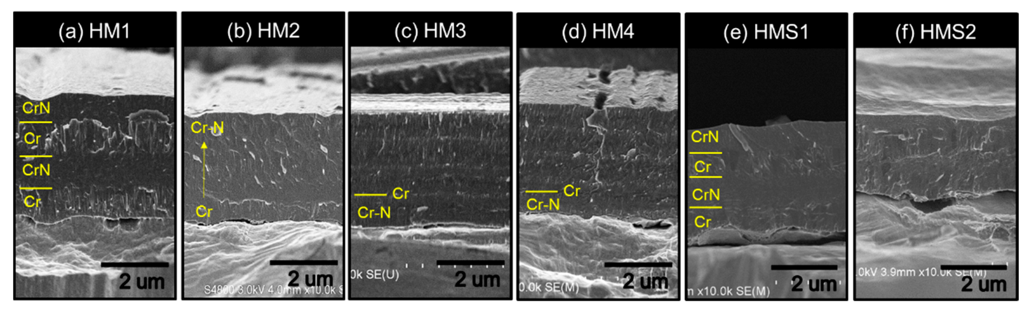
Expanding upon the impact of adjusting the gas flow rate to create various multilayer coatings, the cross-section SEM image of these coatings is shown in Figure 5. In Figure 5a, the NM1 sample is presented, featuring alternating Cr and CrN layers. The interface between each layer is clearly defined, indicating that the Cr bottom layer possessed a conspicuous columnar structure, while the top layer of CrN displayed a fine, dense and uniform structure. Figure 5b shows that the HM2 sample exhibited a featureless appearance due to the gradual increase in nitrogen flow rate throughout the disposition process. As for the HM3 and HM4 coating, as illustrated in Figure 5c,d, the Ar/N2 flow rates were systematically adjusted in a gradual and alternating manner while the total flow ratio was kept constant. The SEM images unveil a dense and fine columnar microstructure, with the columnar structures growing progressively from the bottom to the top of the entire film. The cross-section SEM of the HMS1 and HMS2 samples with a HIPIMS Cr seed layer, obtained at substrate bias of −600 and −900 V, is presented in Figure 5e,f. When compared to the HM1 samples, it is apparent that the Cr layer in the middle still retained a dense columnar structure but with thinner columns in the HMS1 sample, as shown in Figure 5e. Conversely, the interface between each layer in the HMS2 sample was less indistinct, resulting in a more uniform coating, as shown in Figure 5f. It is evident that the elevated substrate bias can lead to an increase in substrate temperature, resulting in higher-quality coating production. However, it is worth noting that a wider gap between the substrate and coatings was observed in the HMS1 and HMS2 samples due to the reduced adhesion strength caused by elevated temperature.
3.4. Electrochemical Corrosion Properties
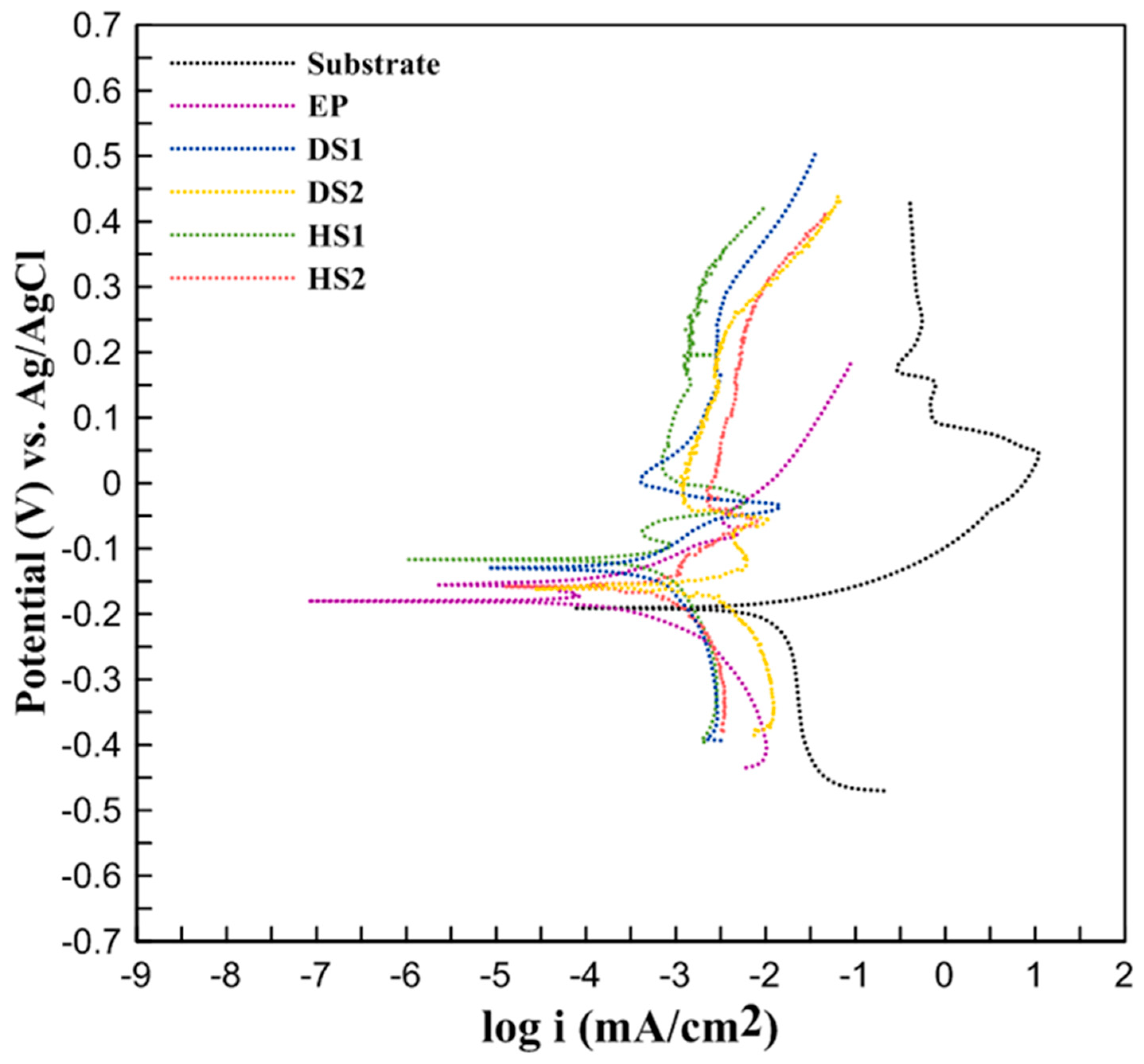
By employing the DC polarization test, the obtained values for corrosion potential (Ecorr) and corrosion current (Icorr) can serve as quantitative indicators of corrosion resistance. The DC polarization curve, along with the corresponding Ecorr and Icorr values, for the brass substrate, the electroplating sample, and the PVD single-layer coated samples in the CASS solution, are illustrated in Figure 6 and summarized in Table 5. These results reveal that the coatings deposited through traditional electroplating, DCMS, and HIPIMS processes provide varying degrees of elective corrosion protection. When comparing the corrosion resistance of PVD-coated samples, it becomes evident that the HS1 and HS2 single-layer coated samples exhibit superior corrosion performance compared to the DCMS samples. This improvement is attributed to the fact that the HIPIMS sample features a fine, dense, and uniform microstructure, as evident in the cross-section SEM images (Figure 4d,e).
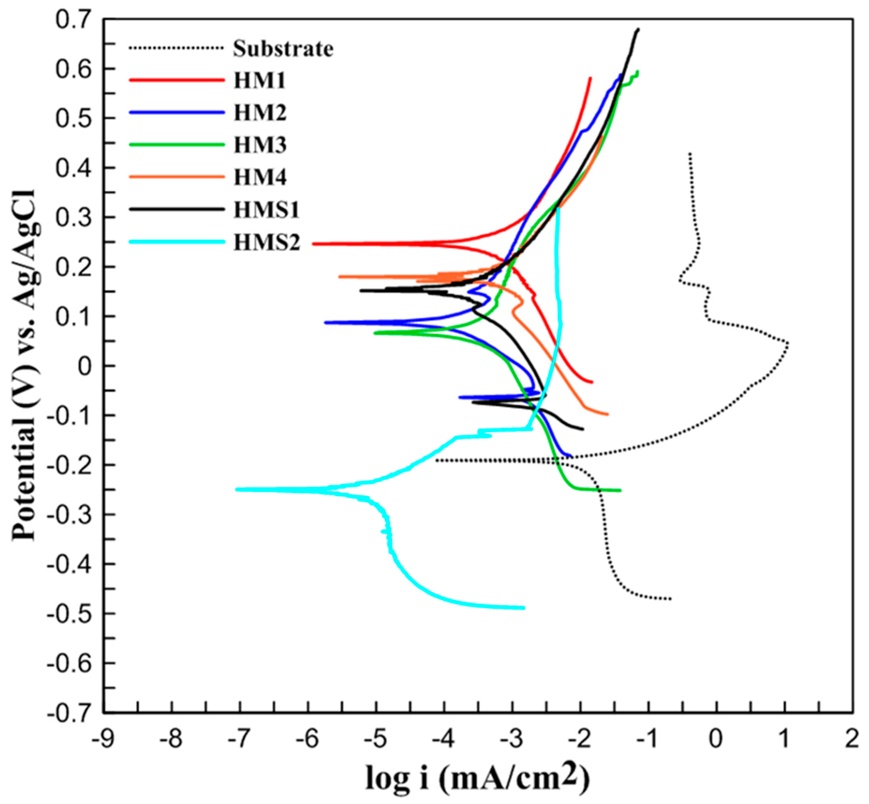
Comparing the DC polarization curves for all multilayer coatings in the CASS solution, as shown in Figure 7 and summarized in Table 6, it is evident that the multilayer structure considerably enhanced corrosion resistance when contrasted with single-layer structures. This improvement can be attributed to the alternating layer structure in the HM1 sample, which can act as a barrier to block through-thickness holes and voids. The relatively high initial potential value (246 mV for Ecorr) is attributed to the prolonged time required for the CASS solution to reach the specimen’s substrates via diffusion through small surface defects. Conversely, distinct corrosion resistance characteristics are observed in the HMS1 and HMS2 samples with the HIPIMS Cr seed layer. The Icorr of both these samples is lower compared to the HM1 sample. This improvement can be attributed to the virtually defect-free coatings resulting from increased argon ion bombardment and substrate bias during the HIPIMS process. However, it is worth noting that the corrosion potential of the HMS2 sample (Ecorr at −243 mV) was even lower than that of the uncoated substrate (Ecorr at −193 mV). This effect might be attributed to the dezincification of the brass substrate in a vacuum environment due to substrate heating [32]. During the process of zinc diffusion out of brass when exposed to heating in a vacuum, a Kirkendall effect takes place. This effect signifies that the outward flux of zinc atoms through the brass is greater than the inward flux of copper atoms. This phenomenon can lead to the multiplication and accumulation of dislocations, as well as the formation of cracks and voids within the alloy. These issues arise due to the unequal diffusion rates of zinc and copper and contribute to the overall degradation of the materials.
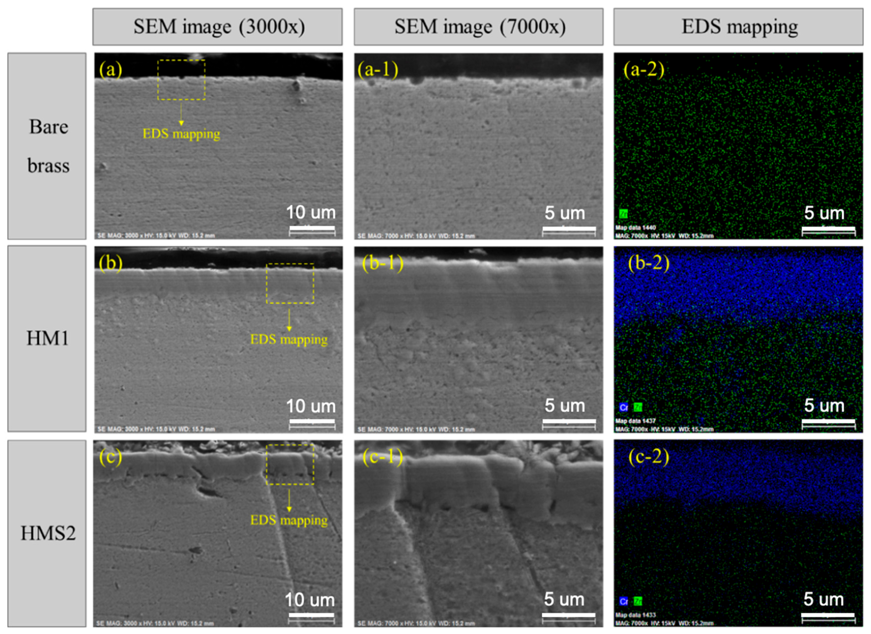
To explore the distribution of chemical compositions, SEM images and EDS elemental mapping measurements were employed to examine the bare brass, HM1 and HMS2 samples, as presented in Figure 8. Comparing the bare brass and HM1 sample to the HMS2 sample, it becomes apparent that voids were formed at the interface between the Cr-N coatings and the substrate, as shown in Figure 8a–c. The presence of voids in this type of interface can be attributed to Kirkendall voids, as mentioned before. These voids are expected to reduce the fracture strength of the interface region, subsequently leading to diminished film adhesion [33]. Figure 8(a-2,b-2) reveals that the Zn distribution appeared to be uniform according to the EDS elemental mapping analysis. However, in the case of the HSM2 sample, there is a noticeable reduction in the Zn content, particularly at the interface between the coating and the substrate, as illustrated in Figure 8(c-2). To further investigate the dezincification in more detail, the coatings were removed by grinding and subsequently analyzed via EDS. The results are shown in Table 7. The chemical compositions of the substrate of the brass and HM1 sample without coatings were approximately Cu:Zn 66:34 ± 2 at %. In contrast, the substrate HSM sample exhibited dezincification, with a composition of Cu:Zn 70:30 ± 2 at %.
3.5. CASS Long-Term Test
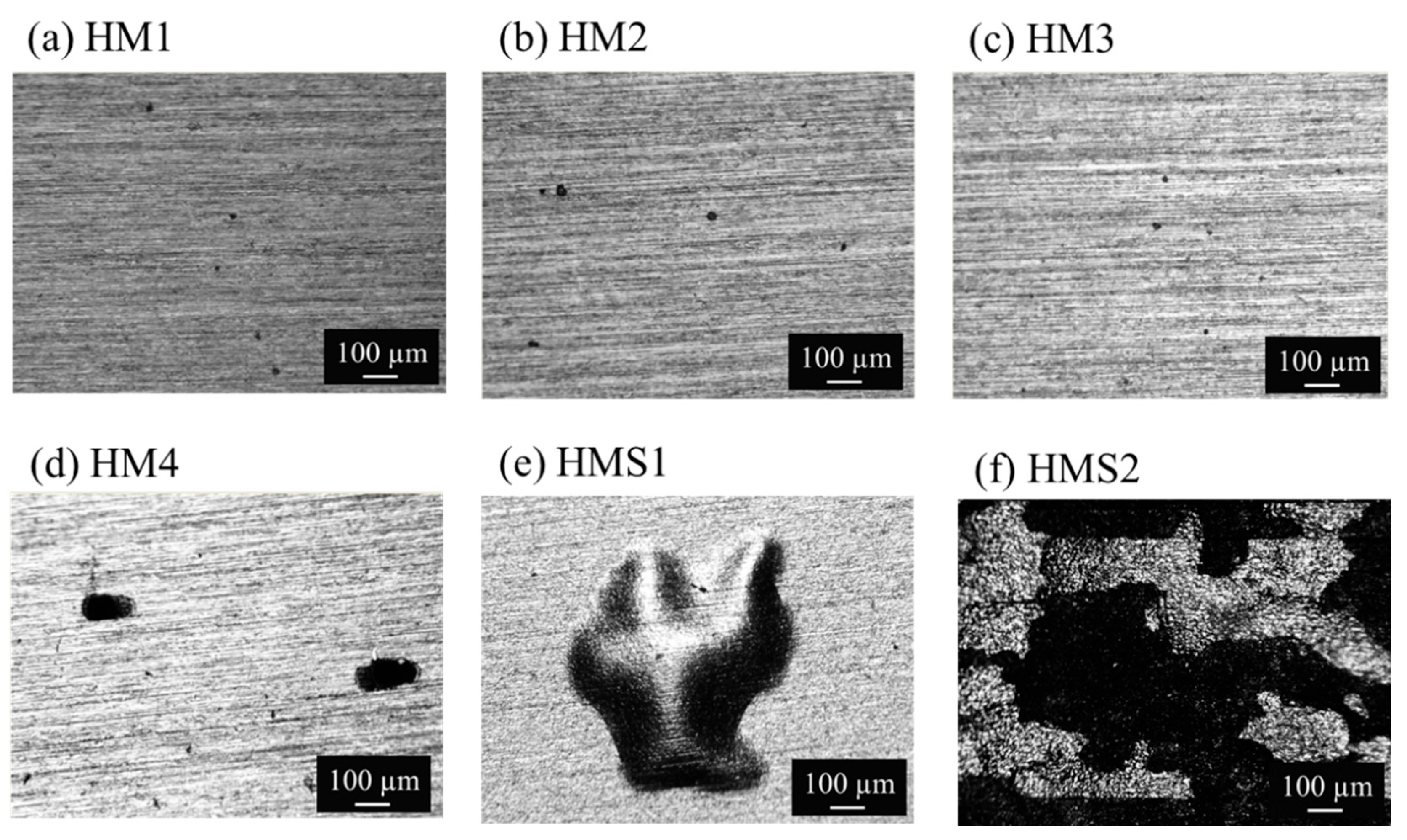
Figure 9 shows the surface appearance observed through optical microscopy of both the bare brass and coated samples after undergoing a 4 h CASS field test. In Figure 9a, the surface morphology of the bare brass exhibited uniform corrosion. Figure 9b through Figure 9f show the optical microscopy morphology of the corroded surface of the electroplated Cr/Ni/Cu and Cr-N single-layer samples prepared through the use of DCMS and HIPIMS. In these cases, pits formed as a consequence of corrosion attacks resulting from galvanic corrosion between the coating and the substrate via the existing defects. When compared to the single-layer coated samples, the Cr-N multilayer samples significantly extend the corrosion resistance period to 8 h. Notably, the size of corrosion pits is noticeably reduced, as shown in Figure 10a–d.
The HMS1 sample (Figure 10e) and the HSM2 (Figure 10f) sample, prepared with a HIPIMS Cr seed layer at substrate bias of −600 and −900 V, displayed distinct corrosion morphologies on the surface after a 4 h CASS test. For HMS1 and HMS2 samples, a higher bias voltage of 600 and 900 V using Ar plasma was applied before multilayer film deposition. The enhanced plasma sheath with Ar plasma led to accelerated Cr ions bombarding the substrate, which is expected to significantly increase the substrate temperature. The rise in substrate temperature, induced by high-energy ion bombardment, has the potential to degrade the physical properties and morphology of the substrate. Consequently, the higher temperature resulting from ion bombardment is believed to degrade the brass substrate in this work due to the dezincification effect at high temperatures, as mentioned in Section 3.4. The DC polarization curves clearly reveal that the corrosion resistance of the HMS2 sample was even worse compared to the brass substrate without any coatings. Furthermore, as shown in Figure 5e–f, the adhesion between coatings and substrate became weaker when high ion bombardment of Cr ion was applied. The variation shown in Figure 10e,f, compared to other multilayer CrN coatings, can be attributed to the elevated substrate temperature resulting from the high ion bombardment energy during deposition, leading to alterations in the mechanical properties and a reduction in adhesion between the coating and the substrate.
The failure in corrosion resistance is linked to insufficient adhesion to the substrate. When the CASS solution comes into direct contact with the substrate surface, it can lead to brass passivation or the formation of corrosion products beneath the film. Ultimately, this can result in the cracking and spallation of the coatings from the surface.
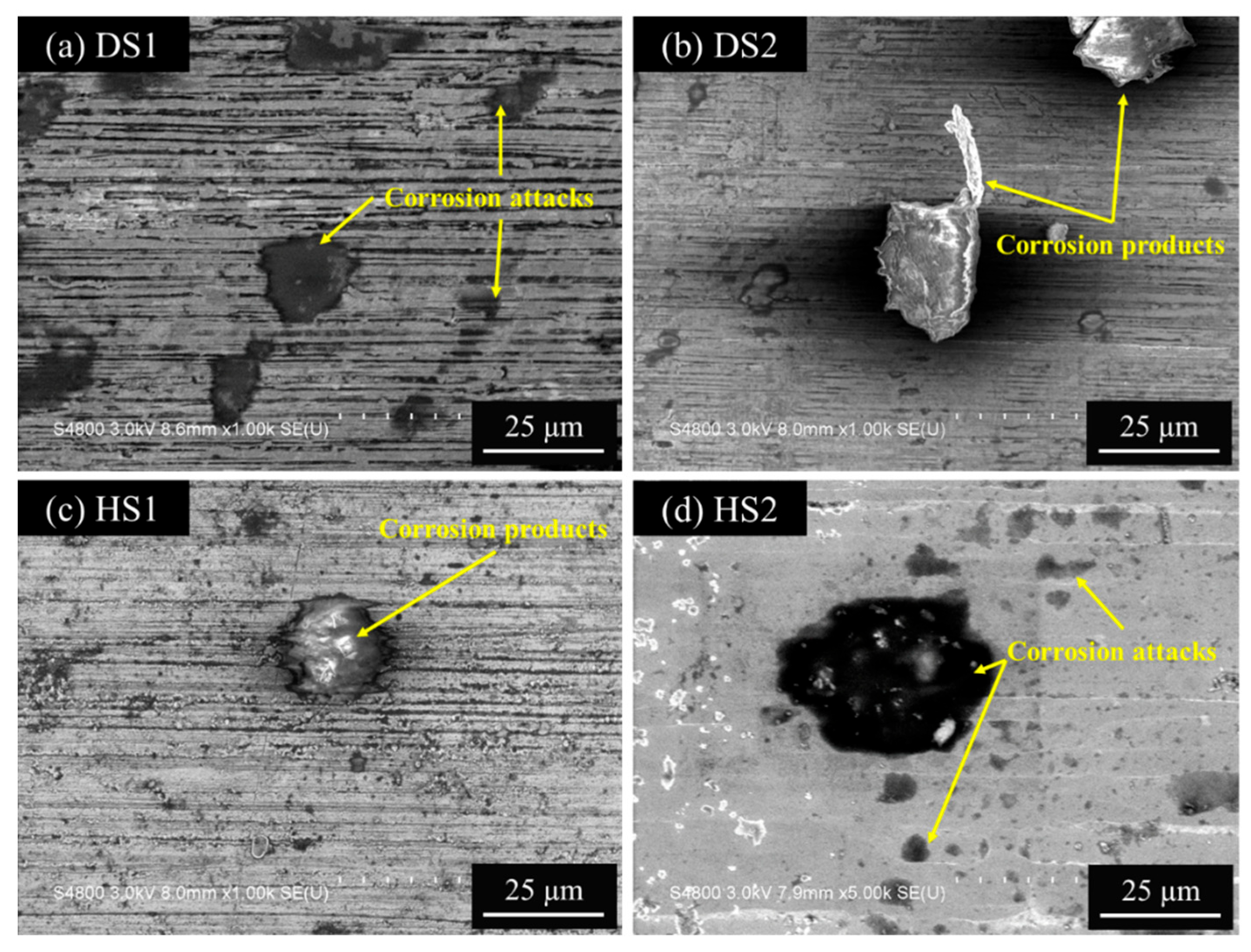
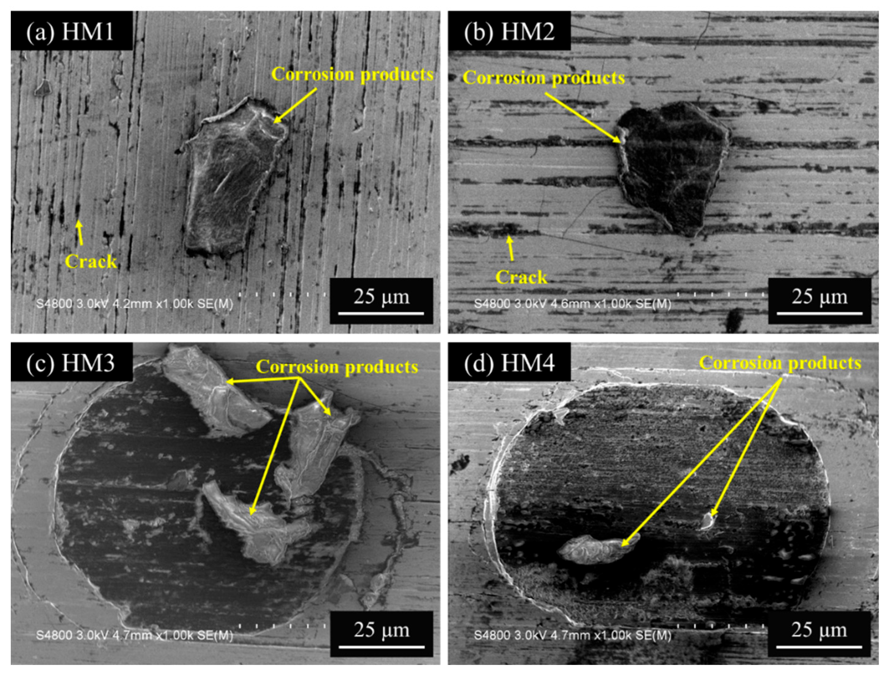
Figure 11 and Figure 12 show the SEM images of the Cr-N single-layer and multilayer-coated samples after the CASS test. It is evident that different types of corrosion morphology are observed for single and multilayer coatings. In the case of DCMS coatings, as shown in Figure 11a,b, the coating experiences a collapse due to interface failure caused by corrosion at the interface between the coating and the substrate. For the HIPIMS coatings, as shown in Figure 11c,d, corrosion pits also formed. However, the dense microstructure of HIPIMS coatings plays a significant role in restricting or even halting the transport of electrolytes to the substrate, thereby reducing or even stopping the corrosion kinetics. Figure 12 presents the SEM images of HIPIMS multilayer samples after 8 h CASS field test. The improved anti-corrosion performance of the multilayered coating, when compared to its single-layer counterparts, can be attributed to the formation of new interfaces. These interfaces are likely to permit the lateral spreading of the corrosive agent, as shown in Figure 12c,d, rather than direct penetration into the substrate. This lateral spreading of the corrosion medium leads to a slower corrosion rate in multilayered coatings, whereas it can directly penetrate the substrate in single-layer coatings. Consequently, the time needed for the corroding medium to reach the substrate, either by penetrating through single-layer coatings (less time) or multilayer coatings (more time), varies. This difference in timing affects the overall corrosion protection effectiveness.
4. Conclusions
In this work, the crystallographic structure, microstructure and corrosion behavior of brass surfaces coated with the chromium nitride (CrN) films through the use of HIPIMS were studied. The conclusions based on the obtained results are as follows:
- In this study, HIPIMS has proven to be effective in producing coatings with a dense, fine and uniform microstructure, as well as reducing columnar growth.
- The CrNx thin films with varying N content (0–36 sccm) can be prepared by adjusting the N2 partial pressure. The alternation in the N2 flow rate led to changes in the chemical composition, phase formation, microstructure, and related properties, as supported by the material characterizations.
- HIPIMS single-layer samples (HS1) exhibited superior corrosion resistance (Ecorr = −109 mV) in comparison to the electroplated (Ecorr = −180 mV) and DCMS (Ecorr = −129 mV) samples, primarily due to their denser microstructure.
- Multilayer coatings without applying high voltage Cr bombardment displayed enhanced corrosion resistance (Ecorr = 246 mV) when compared to the single-layer samples (Ecorr = −109 mV). This improvement is likely attributed to the growth defects occurring in the case of the single layer being neutralized or masked by the successively deposited coating layers. This elongates or obstructs the path for corrosion agents, enhancing the overall resistance to corrosion.
- From the results of the CASS field test, HIPIMS and DCMS single-layer samples exhibited numerous corrosion pits on the surface after a 4 h CASS testing period. In contrast, the multilayer-structured samples managed to withstand the test for a full 8 h, demonstrating extended corrosion protection. However, the multilayer coatings with a HIPIMS Cr seed layer prepared at high substrate bias displayed reduced corrosion protection. The findings suggest that the multilayered CrN coatings prepared through the use of HIPIMS hold potential as materials for applications in decorative finishing that demand corrosion resistance.
Supplementary Materials
The following supporting information can be downloaded at: https://www.mdpi.com/article/10.3390/coatings13122101/s1, Figure S1: Schematic of the parameter setups and variation as a function of deposition time for the Cr single-layer coating (HS1); Figure S2: Schematic of the parameter setups and variation as a function of deposition time for the CrN sin-gle-layer coating (HS2); Figure S3: Schematic of the parameter setups and variation as a function of deposition time for the multilayer CrN coating (HM1); Figure S4: Schematic of the parameter setups and variation as a function of deposition time for the multilayer CrN coating (HM2); Figure S5: Schematic of the parameter setups and variation as a function of deposition time for the multilayer CrN coating (HM3); Figure S6: Schematic of the parameter setups and variation as a function of deposition time for the multilayer CrN coating (HM4); Figure S7: Schematic of the parameter setups and variation as a function of deposition time for the multilayer CrN coating (HMS1); Figure S8: Schematic of the parameter setups and variation as a function of deposition time for the multilayer CrN coating (HMS2).
Author Contributions
Conceptualization, S.-N.H. and J.-L.H.; methodology, S.-N.H. and J.-L.H.; Validation, S.-N.H. and J.-L.H.; investigation, Y.-C.L.; formal analysis, Y.-C.L.; resources, Y.-H.C. and P.-Y.H.; data curation, Y.-C.L.; writing —origin draft preparation, Y.-C.L.; writing —review and editing, S.-N.H.; visualization, Y.-C.L.; supervision, J.-L.H.; project administration, S.-N.H. and J.-L.H.; funding acquisition, S.-N.H. All authors have read and agreed to the published version of the manuscript.
Funding
This research received no external funding.
Institutional Review Board Statement
Not applicable.
Informed Consent Statement
Not applicable.
Data Availability Statement
Data are contained within the article and Supplementary Materials.
Conflicts of Interest
The authors declare no conflict of interest.
References
- 2002/95/EC; Restriction of Hazardous Substances in Electrical and Electronic Equipment. European Commission: Brussel, Belgium, 2003.
- 2002/96/EC; Waste Electrical and Electronic Equipment (WEEE). European Commission: Brussel, Belgium, 2003.
- Munz, W.-D.; Donohue, L.A.; Hovsepian, P. Properties of various large-scale fabricated TiAlN- and CrN-based superlattice coatings grown by combined cathodic arc–unbalanced magnetron sputter deposition. Surf. Coat. Technol. 2000, 125, 269–277. [Google Scholar] [CrossRef]
- Bertrand, G.; Savall, C.; Meunier, C. Properties of reactively RF magnetron-sputtered chromium nitride coatings. Surf. Coat. Technol. 1997, 96, 323–329. [Google Scholar] [CrossRef]
- Chen, Z.-Y.; Li, Z.-Q.; Meng, X.-H. Structure, hardness and corrosion behavior of a gradient CrNx thick coating applied to turbine blades. Appl. Surf. Sci. 2009, 255, 7408–7413. [Google Scholar] [CrossRef]
- Yi, P.; Zhu, L.; Dong, C.; Xiao, K. Corrosion and interfacial contact resistance of 316L stainless steel coated with magnetron sputtered ZrN and TiN in the simulated cathodic environment of a proton-exchange membrane fuel cell. Surf. Coat. Technol. 2019, 363, 198–202. [Google Scholar] [CrossRef]
- Tripathi, U.; Kumar, A.; Kumar, A.; Mulik, R.S. Electrochemical characteristics of sputter deposited ZrN nanoflowers coating for enhanced wetting and anti-corrosion properties. Surf. Coat. Technol. 2022, 440, 128466. [Google Scholar] [CrossRef]
- Liu, C.; Leyland, A.; Bi, Q.; Matthews, A. Corrosion resistance of multi-layered plasma-assisted physical vapour deposition TiN and CrN coatings. Surf. Coat. Technol. 2001, 141, 164–173. [Google Scholar] [CrossRef]
- Olaya, J.J.; Rodil, S.E.; Muhl, S.; Huerta, L. Influence of the energy parameter on the microstructure of chromium nitride coatings. Surf. Coat. Technol. 2006, 200, 5743–5750. [Google Scholar] [CrossRef]
- Guimaraes, M.C.R.; de Castilho, B.C.N.M.; de Souza Nossa, T.; Avila, P.R.T.; Cucatti, S.; Alvarez, F.; Garcia, J.L.; Pinto, H.C. On the effect of substrate oscillation on CrN coatings deposited by HiPIMS and dcMS. Surf. Coat. Technol. 2018, 340, 112–120. [Google Scholar] [CrossRef]
- Vetter, J.; Stüber, M.; Ulrich, S. Growth effects in carbon coatings deposited by magnetron sputtering. Surf. Coat. Technol. 2003, 168, 169–178. [Google Scholar] [CrossRef]
- Čekada, M.; Panjan, P.; Kek-Merl, D.; Panjan, M.; Kapun, G. SEM study of defects in PVD hard coatings. Vacuum 2007, 82, 252–256. [Google Scholar] [CrossRef]
- Wang, H.; Stack, M.; Lyon, S.; Hovsepian, P.; Münz, W.-D. The corrosion behaviour of macroparticle defects in arc bond-sputtered CrN/NbN superlattice coatings. Surf. Coat. Technol. 2000, 126, 279–287. [Google Scholar] [CrossRef]
- Anders, A.; Yang, Y. Plasma studies of a linear magnetron operating in the range from DC to HiPIMS. J. Appl. Phys. 2018, 123, 043302. [Google Scholar] [CrossRef]
- Hnilica, J.; Klein, P.; Vasina, P.; Snyders, R.; Britun, N. Revisiting particle dynamics in HiPIMS discharges. II. Plasma pulse effects. J. Appl. Phys. 2020, 128, 043304. [Google Scholar] [CrossRef]
- Bai, H.; Li, J.; Gao, J.; Ni, J.; Bai, Y.; Jian, J.; Zhao, L.; Bai, B.; Cai, Z.; He, J.; et al. Comparison of CrN Coatings Prepared Using High-Power Impulse Magnetron Sputtering and Direct Current Magnetron Sputtering. Materials 2023, 16, 6303. [Google Scholar] [CrossRef]
- Oje, A.M.; Ogwu, A.A.; Oje, A.I.; Tsendzughul, N.; Rahman, S.U. A comparative study of the corrosion and ion release behaviour of chromium T oxide coatings exposed to saline, Ringer’s and Hank’s physiological solutions. Corros. Sci. 2020, 167, 108533. [Google Scholar] [CrossRef]
- Pan, T.J.; Dai, Y.J.; Jiang, J.; Xiang, J.H.; Yang, Q.Q.; Li, Y.S. Anti-corrosion performance of the conductive bilayer CrC/CrN coated 304SS bipolar plate in acidic environment. Corros. Sci. 2022, 206, 110495. [Google Scholar] [CrossRef]
- Li, Q.; Yang, L.; Wang, Z.; Zhang, H.; Liu, Z.; Chen, Q. The superior properties of CrN coatings prepared by high power pulsed reactive magnetron sputtering. AIP Adv. 2020, 10, 015125. [Google Scholar] [CrossRef]
- Zhang, D.; Zuo, X.; Wang, Z.; Li, H.; Chen, R.; Wang, A.; Ke, P. Comparative study on protective properties of CrN coatings on the ABS substrate by DCMS and HiPIMS techniques. Surf. Coat. Technol. 2020, 394, 125890. [Google Scholar] [CrossRef]
- Zhu, Y.-J.; Ma, J.-L.; Wang, G.-X.; Song, K.-X.; Stock, H.R. Corrosion behaviour of multilayer CrN coatings deposited by hybrid HIPIMS after oxidation treatment. Nanotechnol. Rev. 2020, 9, 596–609. [Google Scholar]
- Anders, A. Deposition rates of high power impulse magnetron sputtering: Physics and economics. J. Vac. Sci. Technol. A 2010, 28, 783–790. [Google Scholar] [CrossRef]
- Brenning, N.; Butler, A.; Hajihoseini, H.; Rudolph, M.; Raddu, M.A.; Gudmundsson, J.T.; Minea, T.; Lundin, D. Optimization of HiPIMS discharges: The selection of pulse power, pulse length, gas pressure, and magnetic field strength. J. Vac. Sci. Technol. A 2020, 38, 033008. [Google Scholar] [CrossRef]
- ASTM B368-09; Standard Test Method for Copper-Accelerated Acetic Acid-Salt Spray (Fog) Testing (CASS Test). ASTM International: West Conshohocken, PA, USA, 2014.
- Hála, M.; Čapek, J.; Zabeida, O.; Klemberg-Sapieha, J.E. Hysteresis-free deposition of niobium oxide films by HiPIMS using different pulse management strategies. J. Phys. D Appl. Phys. 2012, 45, 055204. [Google Scholar] [CrossRef]
- Shimizu, T.; Villamayor, M.; Lundin, D.; Helmersson, U. Process stabilization by peak current regulation in reactive high-power impulse magnetron sputtering of hafnium nitride. J. Phys. D Appl. Phys. 2016, 49, 065202. [Google Scholar] [CrossRef]
- Lin, J.; Wu, Z.L.; Zhang, X.H.; Mishra, B.; Moore, J.J.; Sproul, W.D. A comparative study of CrNx coatings Synthesized by dc and pulsed dcmagnetron sputtering. Thin Solid Films 2009, 517, 1887–1894. [Google Scholar] [CrossRef]
- Lin, J.; Sproul, W.D.; Moore, J.J.; Lee, S.; Myers, S. High rate deposition of thick CrN and Cr2N coatings using modulated pulse power (MPP) magnetron sputtering. Surf. Coat. Technol. 2011, 205, 3226–3234. [Google Scholar] [CrossRef]
- Kong, Q.; Ji, L.; Li, H.; Liu, X.; Wang, Y.; Chen, J.; Zhou, H. Composition, microstructure, and properties of CrNx films deposited using medium frequency magnetron sputtering. Appl. Surf. Sci. 2010, 257, 2269–2274. [Google Scholar] [CrossRef]
- Liu, C.; Bi, Q.; Ziegele, H.; Leyland, A.; Matthews, A. Structure and corrosion properties of PVD Cr–N coatings. J. Vac. Sci. Technol. A 2002, 20, 772–780. [Google Scholar] [CrossRef]
- Greczynski, G.; Jensen, J.; Hultman, L. CrNx Films Prepared by DC Magnetron Sputtering and High-Power Pulsed Magnetron Sputtering: A Comparative Study. IEEE Trans. Plasma Sci. 2010, 38, 3046–3056. [Google Scholar] [CrossRef]
- Itoh, I.; Hikage, T. Dezincification Mechanism of Brass in Vacuum at High Temperature. Trans. Jpn. Inst. Met. 1976, 17, 165–169. [Google Scholar] [CrossRef]
- Mattox, D.M. Particle bombardment effects on thin-film deposition: A review. J. Vac. Sci. Technol. A 1989, 7, 1105–1114. [Google Scholar] [CrossRef]
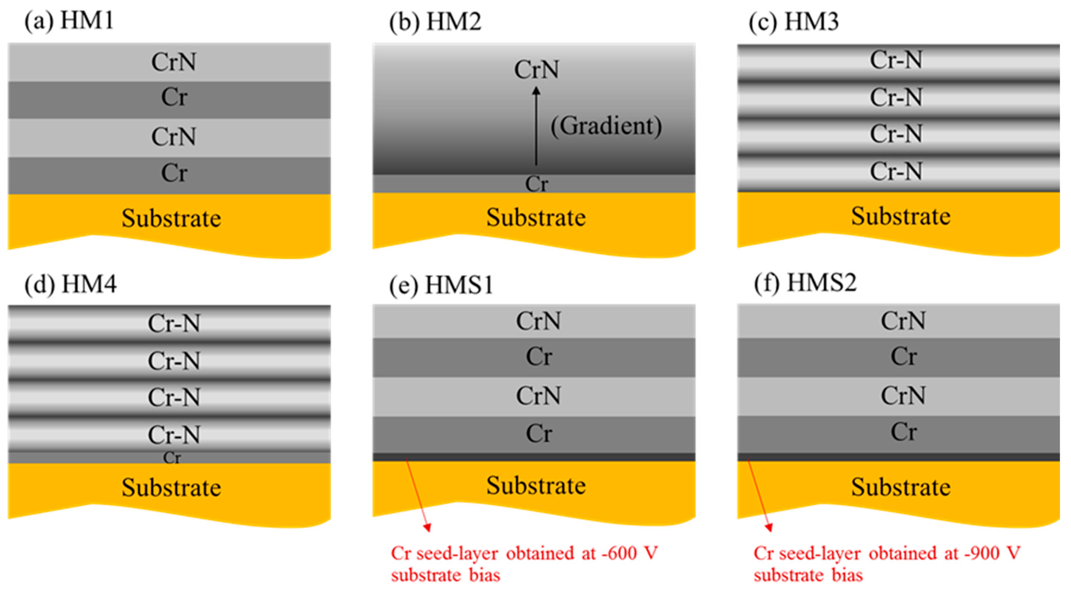
Figure 1.
Schematic drawing of the Cr-N multilayer coatings with different structures deposited via HIPIMS. In (a), Cr/CrN/Cr/CrN four-layer structure, In (b), the flow rate of nitrogen was gradually increased during film deposition, leading to a compositional gradient from bottom to surface of the film. (c) 4 layers with gradient structure; (d) a Cr seed layer inserted between substrate and gradient multilayer., (e) high voltage Cr seed layer (−600 V) inserted between substrate and four-layer structure, and (f) high voltage Cr seed layer (−900 V) inserted between substrate and four-layer structure.

Figure 2.
Current waveform for the HIPIMS experiments with a frequency of 800 Hz and a pulse width of 75 µs for various N2 flows. The inset (a) illustrates the voltage waveform at different N2 flows. The inset (b) plots the peak current observed as a function of N2 flow during discharge.
Figure 2.
Current waveform for the HIPIMS experiments with a frequency of 800 Hz and a pulse width of 75 µs for various N2 flows. The inset (a) illustrates the voltage waveform at different N2 flows. The inset (b) plots the peak current observed as a function of N2 flow during discharge.

Figure 3.
X-ray diffraction pattern for (a) the Cr-N single layer prepared via different PVD processes and (b) the Cr-N multilayer coatings deposited using HIPIMS.
Figure 3.
X-ray diffraction pattern for (a) the Cr-N single layer prepared via different PVD processes and (b) the Cr-N multilayer coatings deposited using HIPIMS.

Figure 4.
Cross-sectional SEM image of the (a) EP, (b) DS1, (c) DS2, (d) HS1 and (e) HS2 samples.

Figure 5.
Cross-sectional SEM images of the Cr-N multilayer coatings deposited using HIPIMS under different Ar/N2 rates. (a) HM1, (b) HM2, (c) HM3, (d) HM4, (e) HMS1 and (f) HMS2.
Figure 5.
Cross-sectional SEM images of the Cr-N multilayer coatings deposited using HIPIMS under different Ar/N2 rates. (a) HM1, (b) HM2, (c) HM3, (d) HM4, (e) HMS1 and (f) HMS2.

Figure 6.
DC Polarization curves of the brass substrate, electroplated, and Cr-N single-layer samples.
Figure 6.
DC Polarization curves of the brass substrate, electroplated, and Cr-N single-layer samples.

Figure 7.
DC Polarization curves of the brass substrate and HIPIMS multilayer samples.

Figure 8.
Cross-sectional SEM images and EDS mapping of the bare brass, HM1 sample and HMS2 samples. The selective areas of EDS mapping shown in (a,b,c) are illustrated in (a-2,b-2,c-2), respectively. The blue and green signal indicates Cr and Zn element, respectively. The highly magnified views of the SEM images are shown in (a-1,b-1,c-1).

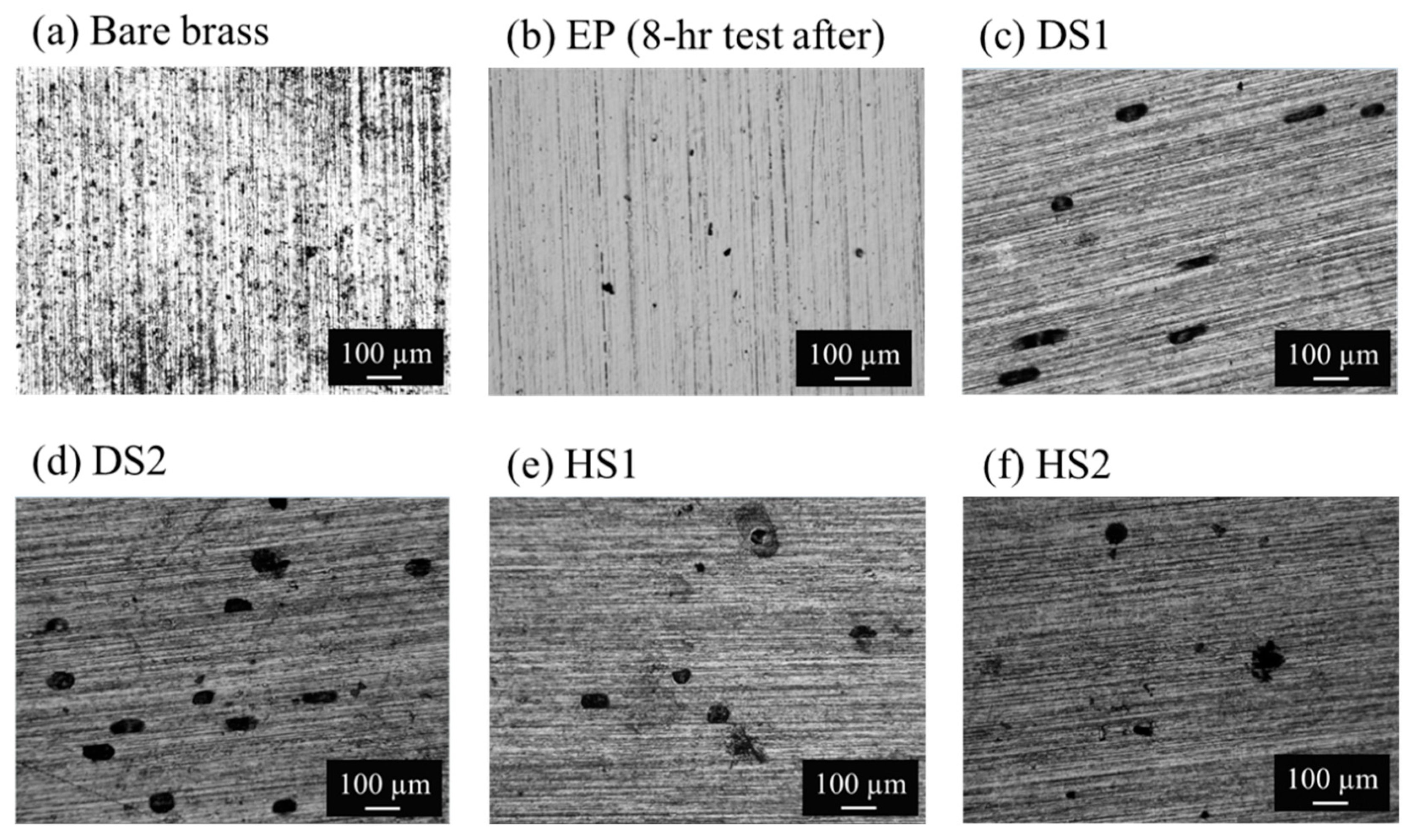
Figure 9.
Optical microscope image of the bare brass and coated samples after a 4 h CASS test, (a) bare brass, (b) EP, (c) DS1, (d) DS2, (e) HS1 and (f) HS2.
Figure 9.
Optical microscope image of the bare brass and coated samples after a 4 h CASS test, (a) bare brass, (b) EP, (c) DS1, (d) DS2, (e) HS1 and (f) HS2.

Figure 10.
Optical microscope image of Cr-N multilayer samples after a 4 h CASS test, (a) HM1, (b) HM2, (c) HM3, (d) HM4, (e) HMS1 and (f) HMS2.
Figure 10.
Optical microscope image of Cr-N multilayer samples after a 4 h CASS test, (a) HM1, (b) HM2, (c) HM3, (d) HM4, (e) HMS1 and (f) HMS2.

Figure 11.
The SEM images of (a) DS1, (b) DS2, (c) HS1 and (d) HS2 samples after a 4 h CASS test.

Figure 12.
The SEM images of (a) HM1, (b) HM2, (c) HM3 and (d) HM4 samples after an 8 h CASS test.


Table 1.
Coated samples and their descriptions.
| Coated Samples and Its Description | ||
|---|---|---|
| No. | Sample Name | Description |
| 1 | EP | Cr/Ni/Cu electroplated sample |
| 2 | DS1 | Cr single layer deposited via DCMS |
| 3 | DS2 | Cr-N single layer deposited via DCMS |
| 4 | HS1 | Cr single layer deposited via HIPIMS |
| 5 | HS2 | Cr-N single layer deposited via HIPIMS |
| 6 | HM1 | Cr-N multilayer deposited via HIPIMS; structure—see Figure 1a |
| 7 | HM2 | Cr-N multilayer deposited via HIPIMS; structure—see Figure 1b |
| 8 | HM3 | Cr-N multilayer deposited via HIPIMS; structure—see Figure 1c |
| 9 | HM4 | Cr-N multilayer deposited via HIPIMS; structure—see Figure 1d |
| 10 | HMS1 | Cr-N multilayer (HM1) with HIPIMS Cr seed layer obtained at −600 V substrate bias; structure—see Figure 1e |
| 11 | HMS2 | Cr-N multilayer (HM1) with HIPIMS Cr seed layer obtained at −900 V substrate bias; structure—see Figure 1f |
Table 2.
Cr-N single-layer deposition parameters.
| Pre-Treatment Condition (Argon Pretreatment Parameters) | ||||
|---|---|---|---|---|
| Working pressure (mTorr) | 9.5 | |||
| Working time (min) | 10 | |||
| Substrate bias (V) | −600 | |||
| Ar flow rate for ion etching (sccm) | 150 | |||
| Cr-N single layer deposition parameters | ||||
| Sample name | DS1 | DS2 | HS1 | HS2 |
| Deposition time (min) | 15 | |||
| Average output power (W) | 6000 | |||
| Ton/Toff (µs) | - | 75/1175 | ||
| Working pressure (mTorr) | 1.5 | |||
| Substrate bias (V) | −80 | |||
| N2/Ar ratio (sccm) | 0/112 | 36/90 | 0/112 | 36/90 |
Table 3.
Cr-N multilayer deposition parameters (HM1 to HM4 samples).
| Pre-Treatment Condition (Argon Pretreatment Parameters) | ||||
|---|---|---|---|---|
| Working pressure (mTorr) | 9.5 | |||
| Working time (min) | 10 | |||
| Substrate bias (V) | −600 | |||
| Ar flow rate for ion etching (sccm) | 150 | |||
| Cr-N single layer deposition parameters | ||||
| Sample name | HM1 | HM2 | HM3 | HM4 |
| Deposition time (min) | 30 | |||
| Average output power (W) | 6000 | |||
| Ton/Toff (µs) | 75/1175 | |||
| Working pressure (mTorr) | 1.5 | |||
| Substrate bias (V) | −80 | |||
| N2/Ar ratio (sccm) | 0/112 and 36/90 | 0/112 to 58/67 | 0/112 to 58/67 | 0/112 to 58/67 |
Table 4.
Cr-N multilayer deposition parameters (HMS1 and HMS2 samples).
| Pre-Treatment Condition (Argon Pretreatment Parameters) | ||
|---|---|---|
| Working pressure (mTorr) | 9.5 | |
| Working time (min) | 10 | |
| Substrate bias (V) | −600 | |
| Ar radio (sccm) | 150 | |
| Cr+ etching (for Cr seed layer) | ||
| Working pressure (mTorr) | 1.5 | |
| Deposition time (min) | 1 | |
| Average output power (W) | 6000 | |
| Substrate bias (V) | −600 | −900 |
| Ton/Toff (µs) | 75/1175 | |
| N2/Ar ratio (sccm) | 0/112 | |
| Cr-N single layer deposition parameters | ||
| Sample name | HMS1 | HM2 |
| Deposition time (min) | 29 | |
| Average output power (W) | 6000 | |
| Ton/Toff (µs) | 75/1175 | |
| Working pressure (mTorr) | 1.5 | |
| Substrate bias (V) | −80 | |
| N2/Ar ratio (sccm) | 0/112 and 36/90 | |
Table 5.
Summarized results of the brass substrate, electroplated and Cr-N single layer within the electrochemical corrosion investigation. The thickness was roughly estimated using cross-section SEM images, as shown in Figure 4.
Table 5.
Summarized results of the brass substrate, electroplated and Cr-N single layer within the electrochemical corrosion investigation. The thickness was roughly estimated using cross-section SEM images, as shown in Figure 4.
| Samples | Thickness (μm) | Corrosion Potential Ecorr (mV) | Corrosion Density Icorr (µA/cm2) | Resistance Polarization Rp (kΩ/cm2) |
|---|---|---|---|---|
| Substrate | - | −193 | 28.294 | 5.7 |
| EP | 10.0 | −180 | 0.085 | 140.5 |
| DS1 | 3.5 | −129 | 1.880 | 63.1 |
| DS2 | 3.0 | −145 | 2.715 | 28.6 |
| HS1 | 2.0 | −109 | 0.602 | 105.1 |
| HS2 | 1.5 | −144 | 0.732 | 86.9 |
Table 6.
Summarized results of the brass substrate and HIPIMS multilayer samples with the electrochemical corrosion investigation. The thickness was roughly estimated using cross-section SEM image as shown in Figure 5.
Table 6.
Summarized results of the brass substrate and HIPIMS multilayer samples with the electrochemical corrosion investigation. The thickness was roughly estimated using cross-section SEM image as shown in Figure 5.
| Samples | Thickness (μm) | Corrosion Potential Ecorr (mV) | Corrosion Density Icorr (µA/cm2) | Resistance Polarization Rp (kΩ/cm2) |
|---|---|---|---|---|
| Substrate | - | −193 | 28.294 | 5.7 |
| HM1 | 3.5 | 246 | 0.471 | 134.7 |
| HM2 | 3.0 | 94 | 0.121 | 295.0 |
| HM3 | 3.5 | 66 | 0.189 | 177.5 |
| HM4 | 3.0 | 181 | 0.327 | 103.5 |
| HMS1 | 3.0 | 152 | 0.265 | 250.8 |
| HMS2 | 2.5 | −243 | 0.008 | 13,143.9 |
Table 7.
Chemical composition of the substrate for Brass substrate, HM1, and HMS1 sample using EDS quotative analysis. The coating of HM1 and HMS1 samples was removed using a grinding process.
Table 7.
Chemical composition of the substrate for Brass substrate, HM1, and HMS1 sample using EDS quotative analysis. The coating of HM1 and HMS1 samples was removed using a grinding process.
| Samples | Cu (at. %) | Zn (at. %) | Error (at. %) |
|---|---|---|---|
| Brass substrate | 66 | 34 | 2 |
| HM1 | 66 | 34 | 2 |
| HMS1 | 70 | 30 | 2 |
Disclaimer/Publisher’s Note: The statements, opinions and data contained in all publications are solely those of the individual author(s) and contributor(s) and not of MDPI and/or the editor(s). MDPI and/or the editor(s) disclaim responsibility for any injury to people or property resulting from any ideas, methods, instructions or products referred to in the content. |
© 2023 by the authors. Licensee MDPI, Basel, Switzerland. This article is an open access article distributed under the terms and conditions of the Creative Commons Attribution (CC BY) license (https://creativecommons.org/licenses/by/4.0/).
Share and Cite
MDPI and ACS Style
Liu, Y.-C.; Hsiao, S.-N.; Chen, Y.-H.; Hsieh, P.-Y.; He, J.-L. High-Power Impulse Magnetron Sputter-Deposited Chromium-Based Coatings for Corrosion Protection. Coatings 2023, 13, 2101. https://doi.org/10.3390/coatings13122101
AMA Style
Liu Y-C, Hsiao S-N, Chen Y-H, Hsieh P-Y, He J-L. High-Power Impulse Magnetron Sputter-Deposited Chromium-Based Coatings for Corrosion Protection. Coatings. 2023; 13(12):2101. https://doi.org/10.3390/coatings13122101
Chicago/Turabian StyleLiu, Yen-Chun, Shih-Nan Hsiao, Ying-Hung Chen, Ping-Yen Hsieh, and Ju-Liang He. 2023. "High-Power Impulse Magnetron Sputter-Deposited Chromium-Based Coatings for Corrosion Protection" Coatings 13, no. 12: 2101. https://doi.org/10.3390/coatings13122101
Note that from the first issue of 2016, this journal uses article numbers instead of page numbers. See further details here.