
Structural, Morphologic, and Ferroelectric Properties of PZT Films Deposited through Layer-by-Layer Reactive DC Magnetron Sputtering

 , and
, and 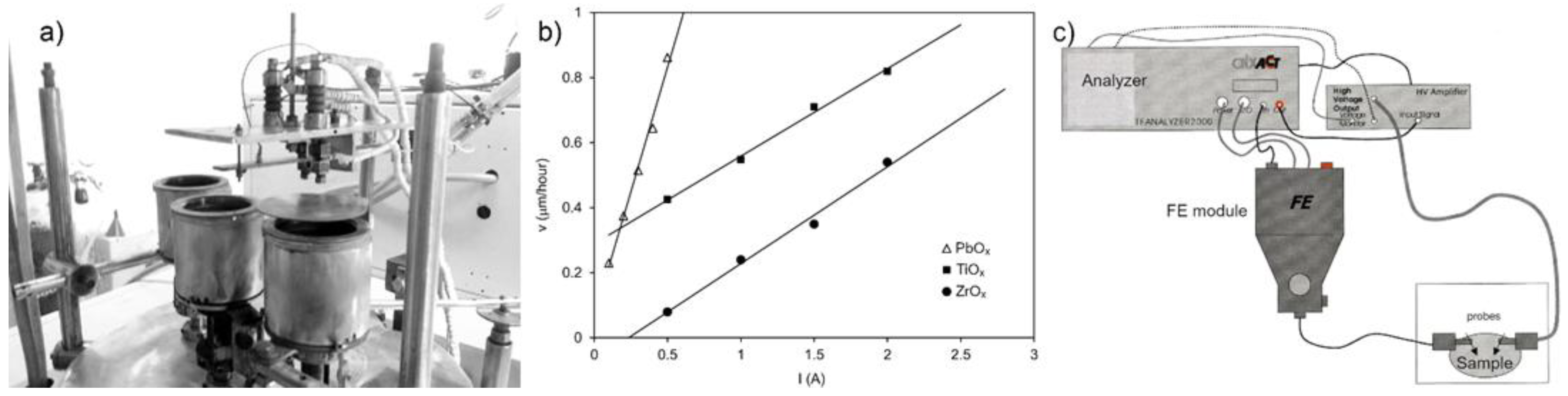
Abstract
:1. Introduction
2. Materials and Methods
3. Results and Discussion
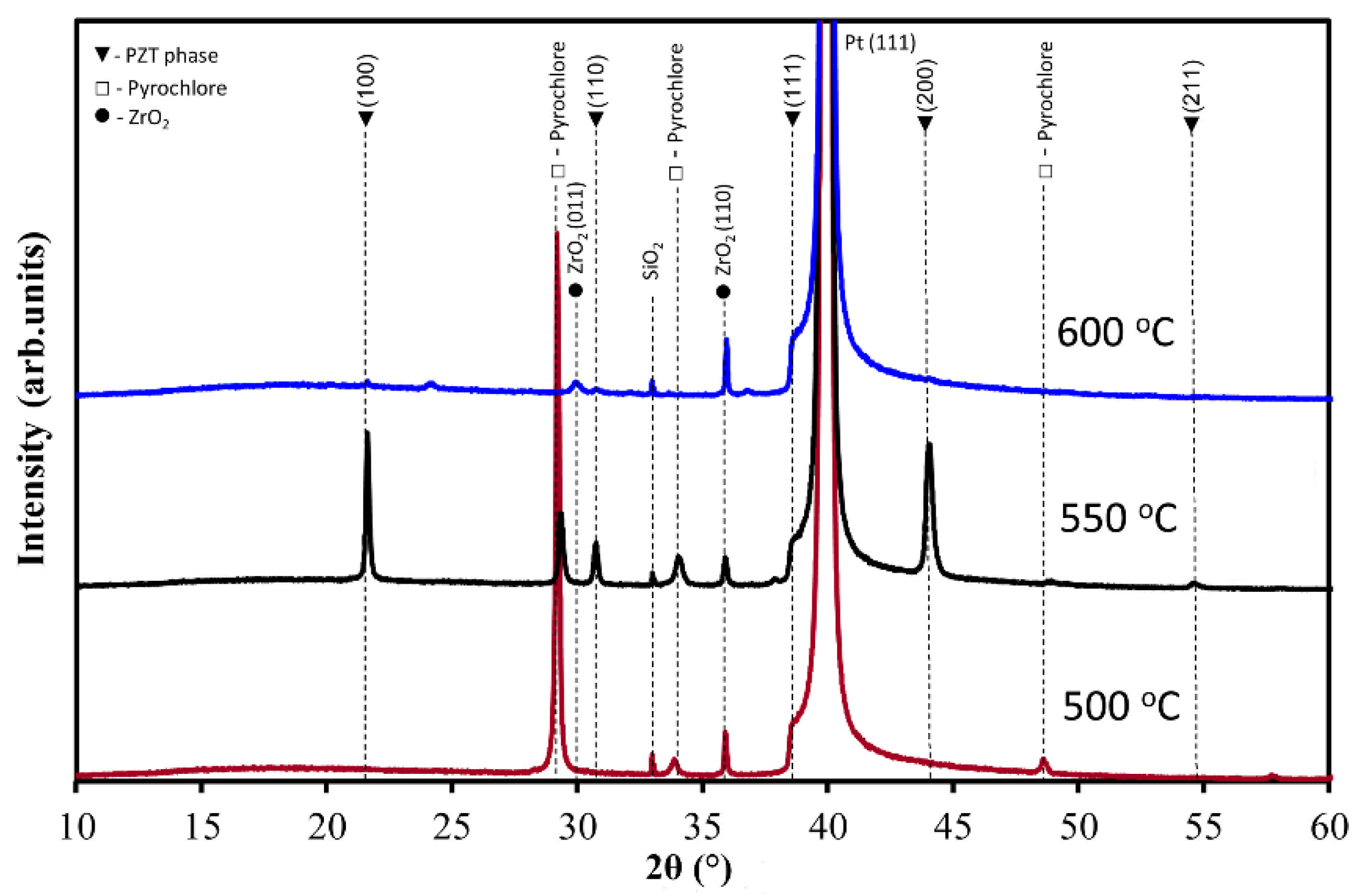
3.1. XRD Analysis
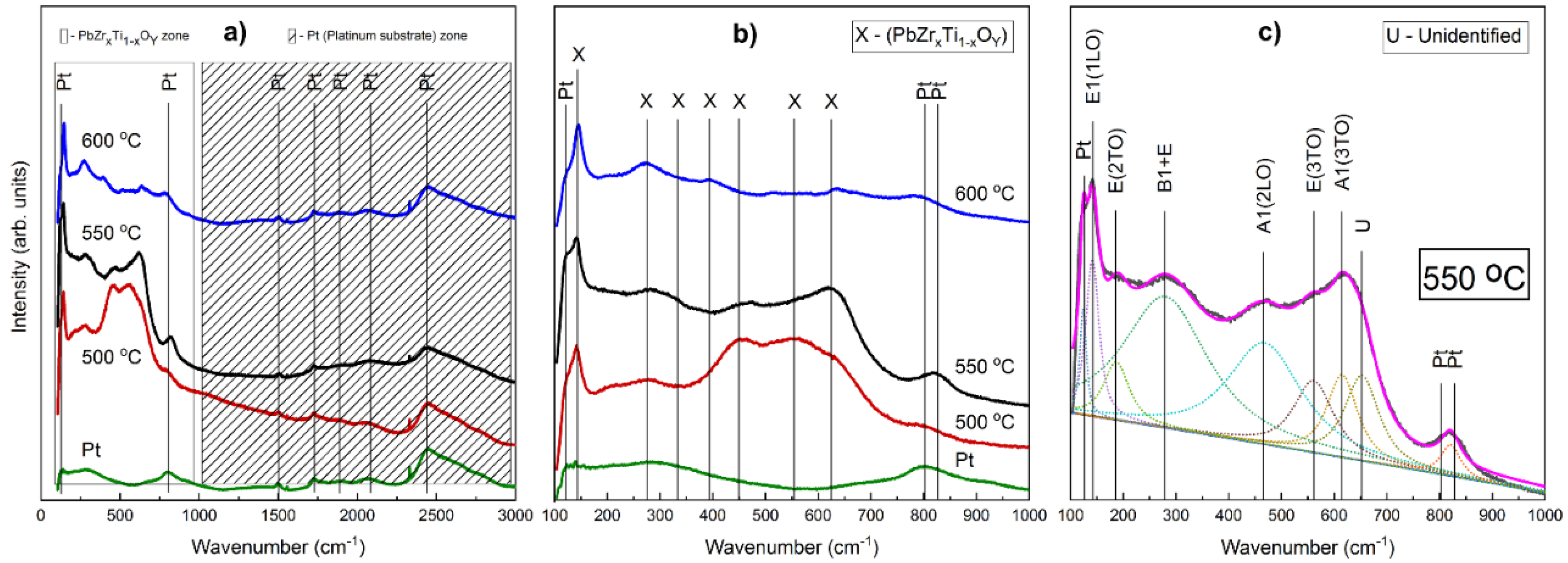
3.2. Raman Spectra Analysis
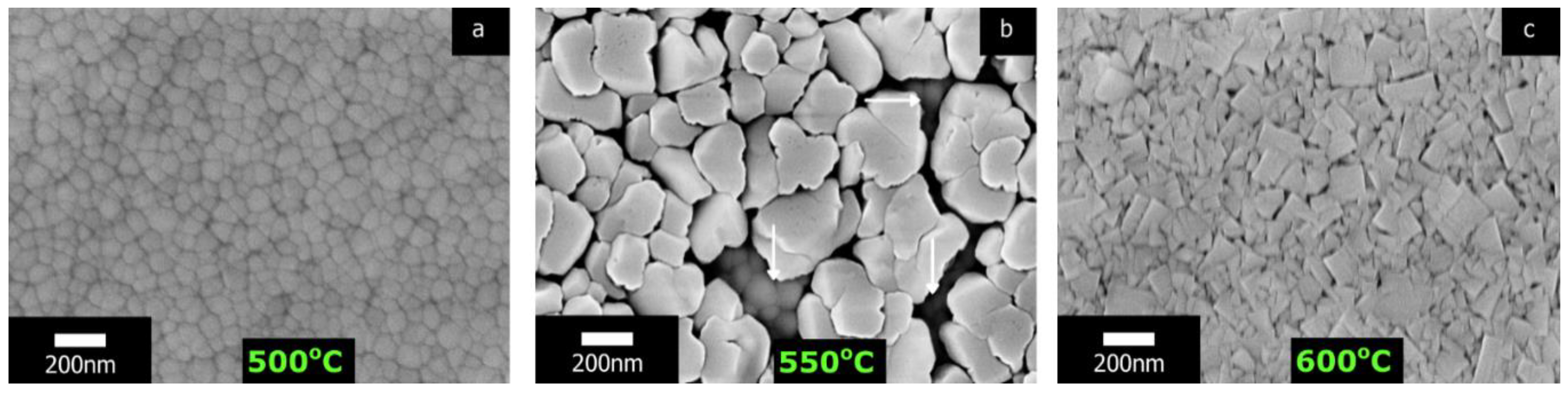
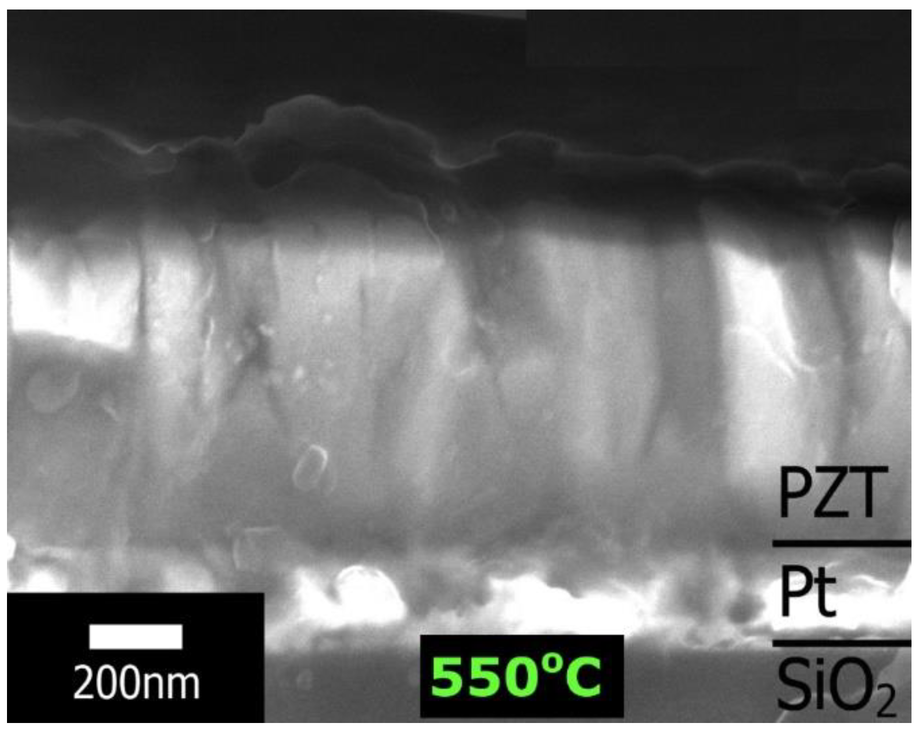
3.3. SEM Analysis
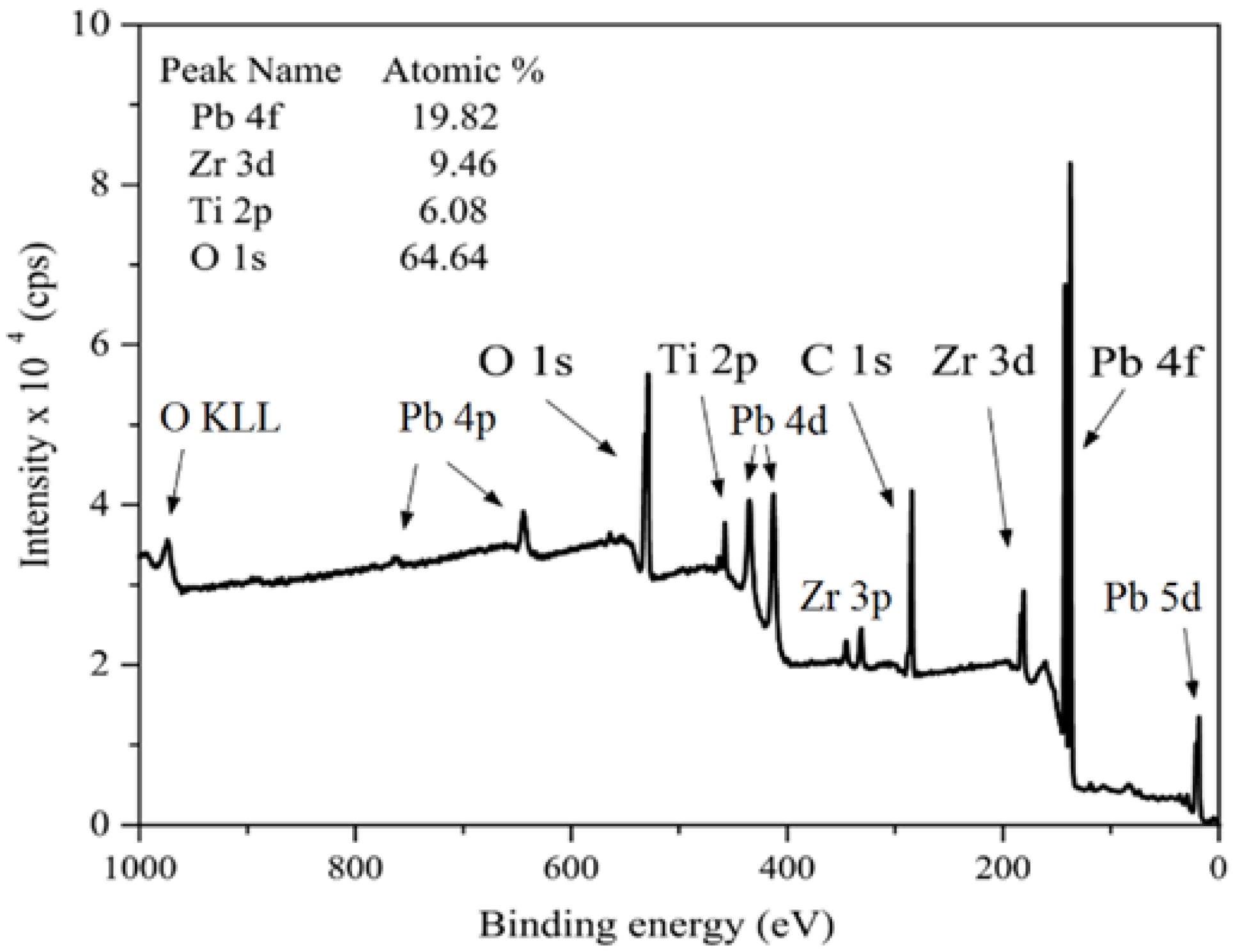
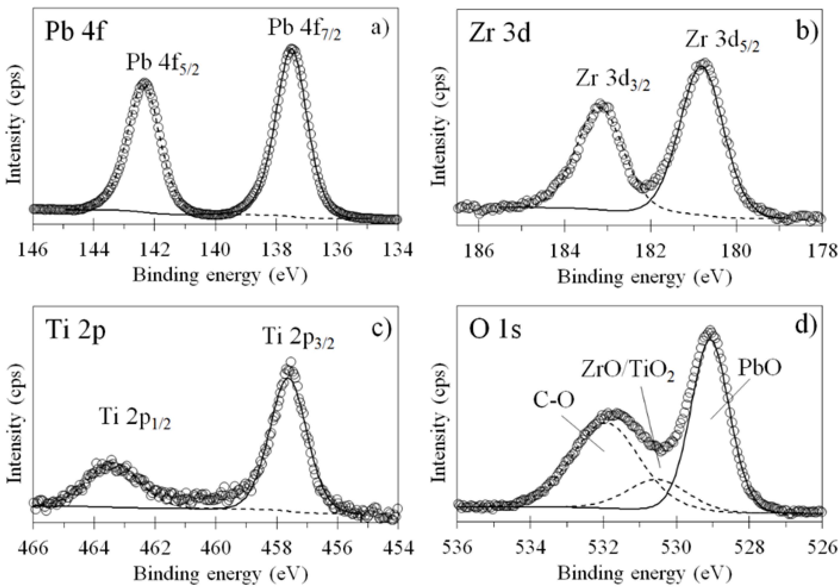
3.4. XPS Analysis
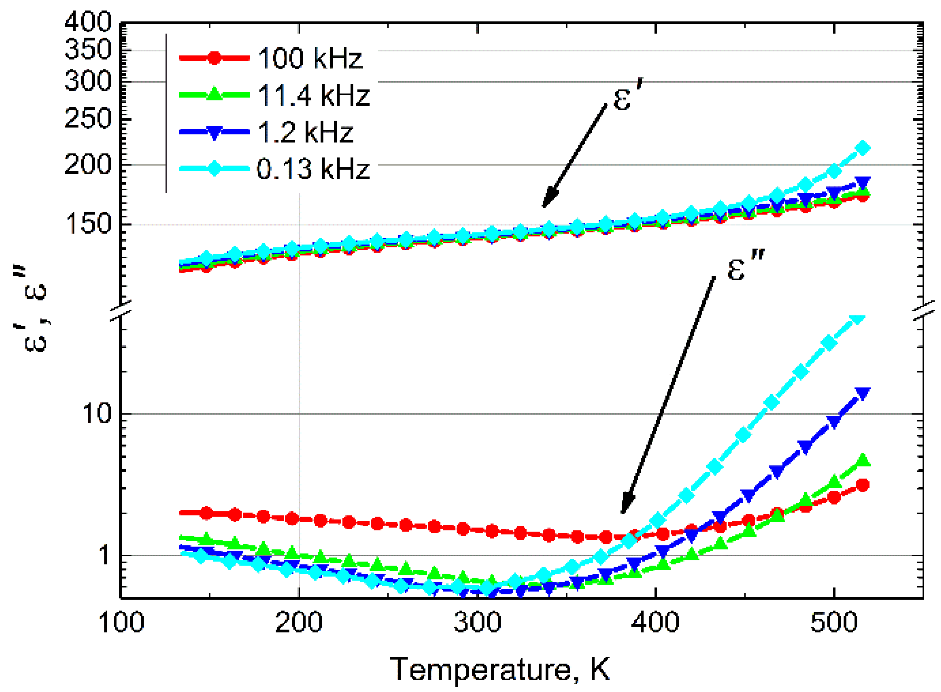
3.5. Analysis of Dielectric Properties
4. Conclusions
Author Contributions
Funding
Institutional Review Board Statement
Informed Consent Statement
Data Availability Statement
Conflicts of Interest
References
- Zhou, Q.; Lau, S.; Wu, D.; Shung, K.K. Piezoelectric films for high frequency ultrasonic transducers in biomedical applications. Prog. Mater. Sci. 2011, 56, 139–174. [Google Scholar] [CrossRef] [PubMed] [Green Version]
- Zribi, A.; Fortin, J.B. Functional Thin Films and Nanostructures for Sensorssynthesis, Physics and Applications; Springer: New York, NY, USA, 2009. [Google Scholar]
- Steinem, C.; Janshoff, A. Piezoelectric Sensors; Springer: Berlin/Heidelberg, Germany, 2007. [Google Scholar]
- Gao, W.; Zhu, Y.; Wang, Y.; Yuan, G.; Liu, J.-M. A review of flexible perovskite oxide ferroelectric films and their application. J. Materiomics 2020, 6, 1–16. [Google Scholar] [CrossRef]
- Sezer, N.; Koç, M. A comprehensive review on the state-of-the-art of piezoelectric energy harvesting. Nano Energy 2020, 80, 105567. [Google Scholar] [CrossRef]
- Ryndzionek, R.; Sienkiewicz, Ł. A review of recent advances in the single- and multi-degree-of-freedom ultrasonic piezoelectric motors. Ultrasonics 2021, 116, 106471. [Google Scholar] [CrossRef]
- Fei, C.; Chen, Z.; Fong, W.M.; Zhu, B.; Wang, L.; Ren, W.; Li, Y.; Shi, J.; Shung, K.K.; Zhou, Q. Modification of microstructure on PZT films for ultrahigh frequency transducer. Ceram. Int. 2015, 41, S650–S655. [Google Scholar] [CrossRef]
- Wixom, A.S.; Anderson, M.J.; Bahr, D.F.; Morris, D.J. A new acoustic transducer with a pressure-deformed piezoelectric diaphragm. Sens. Actuators A Phys. 2012, 179, 204–210. [Google Scholar] [CrossRef]
- Anoop, G.; Seo, J.; Han, C.J.; Lee, H.J.; Kim, G.W.; Lee, S.S.; Park, E.Y.; Jo, J.Y. Ultra-thin platinum interfacial layer assisted-photovoltaic response of transparent Pb(Zr,Ti)O 3 thin film capacitors. Sol. Energy 2015, 111, 118–124. [Google Scholar] [CrossRef]
- Gupta, R.; Gupta, V.; Tomar, M. Ferroelectric PZT thin films for photovoltaic application. Mater. Sci. Semicond. Process. 2019, 105, 104723. [Google Scholar] [CrossRef]
- Chen, M.; Shen, X.; Zhou, C.; Cao, D.; Xue, W. High-performance self-powered visible-blind ultraviolet photodetection achieved by ferroelectric PbZr0.52Ti0.48O3 thin films. J. Alloy Compd. 2021, 897, 163208. [Google Scholar] [CrossRef]
- Bez, R.; Pirovano, A. 1—Overview of non-volatile memory technology: Markets, technologies and trends. In Advances in Non-Volatile Memory and Storage Technology; Nishi, Y., Ed.; Woodhead Publishing: Sawston, UK, 2014; pp. 1–24. [Google Scholar]
- Eshita, T.; Tamura, T.; Arimoto, Y. 14—Ferroelectric random access memory (FRAM) devices. In Advances in Non-Volatile Memory and Storage Technology, Nishi, Y., Ed.; Woodhead Publishing: Sawston, UK, 2014; pp. 434–454. [Google Scholar]
- Mao, D.; Mejia, I.; Salas-Villasenor, A.; Singh, M.; Stiegler, H.; Gnade, B.; Quevedo-Lopez, M. Ferroelectric random access memory based on one-transistor–one-capacitor structure for flexible electronics. Org. Electron. 2013, 14, 505–510. [Google Scholar] [CrossRef]
- Liu, G.; Zhang, S.; Jiang, W.; Cao, W. Losses in ferroelectric materials. Mater. Sci. Eng. R Rep. 2015, 89, 1–48. [Google Scholar] [CrossRef] [PubMed] [Green Version]
- Genenko, Y.; Glaum, J.; Hoffmann, M.J.; Albe, K. Mechanisms of aging and fatigue in ferroelectrics. Mater. Sci. Eng. B 2015, 192, 52–82. [Google Scholar] [CrossRef]
- Wang, Z.; Lai, Z.; Hu, Z. Low-temperature preparation and characterization of the PZT ferroelectric thin films sputtered on FTO glass substrate. J. Alloy Compd. 2013, 583, 452–454. [Google Scholar] [CrossRef]
- Bose, A.; Maity, T.; Bysakh, S.; Seal, A.; Sen, S. Influence of plasma pressure on the growth characteristics and ferroelectric properties of sputter-deposited PZT thin films. Appl. Surf. Sci. 2010, 256, 6205–6212. [Google Scholar] [CrossRef]
- Bose, A.; Sreemany, M.; Bysakh, S. Influence of processing parameters on the growth characteristics and ferroelectric properties of sputtered PZT thin films on stainless steel substrates. Appl. Surf. Sci. 2013, 282, 202–210. [Google Scholar] [CrossRef]
- Sreemany, M.; Bose, A.; Sen, S. Influence of chemical composition, phase and thickness of TiOx (x ≤ 2) seed layer on the growth and orientation of the perovskite phase in sputtered PZT thin films. Mater. Chem. Phys. 2009, 115, 453–462. [Google Scholar] [CrossRef]
- Maurya, K.; Halder, S.; Sen, S.; Bose, A.; Bysakh, S. High resolution X-ray and electron microscopy characterization of PZT thin films prepared by RF magnetron sputtering. Appl. Surf. Sci. 2014, 313, 196–206. [Google Scholar] [CrossRef]
- Borowiak, A.; Niu, G.; Pillard, V.; Agnus, G.; Lecoeur, P.; Albertini, D.; Baboux, N.; Gautier, B.; Vilquin, B. Pulsed laser deposition of epitaxial ferroelectric Pb(Zr,Ti)O3 films on silicon substrates. Thin Solid Films 2012, 520, 4604–4607. [Google Scholar] [CrossRef]
- Pham, M.T.; Boukamp, B.; Bouwmeester, H.; Blank, D. Microstructural and electrical properties of nanocomposite PZT/Pt thin films made by pulsed laser deposition. Ceram. Int. 2004, 30, 1499–1503. [Google Scholar] [CrossRef]
- Lin, Y.; Chuang, H.; Shen, J. PZT thin film preparation by pulsed DC magnetron sputtering. Vacuum 2009, 83, 921–926. [Google Scholar] [CrossRef]
- Shakeri, A.; Abdizadeh, H.; Golobostanfard, M.R. Synthesis and characterization of thick PZT films via sol–gel dip coating method. Appl. Surf. Sci. 2014, 314, 711–719. [Google Scholar] [CrossRef]
- Wang, D.; Chen, C.; Ma, J.; Liu, T. Lead-based titanate ferroelectric thin films fabricated by a sol–gel technique. Appl. Surf. Sci. 2008, 255, 1637–1645. [Google Scholar] [CrossRef]
- Moon, J.-W.; Wakiya, N.; Fujito, K.; Iimori, N.; Kiguchi, T.; Yoshioka, T.; Tanaka, J.; Shinozaki, K. Effect of SrTiO3 seed layer deposition time and thickness on low-temperature crystallization and electrical properties of Pb(Zr, Ti)O3 films by metalorganic chemical vapor deposition. Mater. Sci. Eng. B 2008, 148, 22–25. [Google Scholar] [CrossRef]
- Stankus, V.; Dudonis, J.; Pranevicius, L.; Pranevičius, L.L.; Milcius, D.; Templier, C.; Riviere, J.P. On the mechanism of synthesis of PbTiO3 thin films by thermal annealing of Pb/Ti layers in air at atmospheric pressure. Thin Solid Films 2003, 426, 78–84. [Google Scholar] [CrossRef]
- Iljinas, A.; Stankus, V.; Čyvienė, J.; Abakevičienė, B. Formation of PbTiO3 thin films on seed layers using DC magnetron layer-by-layer deposition. Vacuum 2015, 122, 310–313. [Google Scholar] [CrossRef]
- Iljinas, A.; Stankus, V. Structural and ferroelectric properties of bismuth ferrite thin films deposited by direct current reactive magnetron sputtering. Thin Solid Films 2016, 601, 106–110. [Google Scholar] [CrossRef]
- TF Analyzer 2000 Hysteresis Software, Ed. 2.2.; aixACCT Systems GmbH: Aachen, Germany, 2013.
- Velu, G.; Remiens, D. In situ deposition of sputtered PZT films: Control of the growth temperature by the sputtered lead flux. Vacuum 2000, 56, 199–204. [Google Scholar] [CrossRef]
- Kratzer, M.; Castaldi, L.; Heinz, B.; Mamazza, R.; Kaden, D.; Quenzer, H.J.; Wagner, B. In-situ large scale deposition of PZT films by RF magnetron sputtering. In Proceedings of the 2011 International Symposium on Applications of Ferroelectrics (ISAF/PFM) and 2011 International Symposium on Piezoresponse Force Microscopy and Nanoscale Phenomena in Polar Materials, Vancouver, BC, Canada, 24–27 July 2011; pp. 1–4. [Google Scholar]
- Park, C.-H.; Son, Y.-G.; Won, M.-S. Microstructure and ferroelectric properties of r.f. magnetron sputtering derived PZT thin films deposited on interlayer (PbO/TiO2). Microchem. J. 2005, 80, 201–206. [Google Scholar] [CrossRef]
- Wang, Z.J.; Aoki, Y.; Kokawa, H.; Ichiki, M.; Maeda, R. Effect of Zr/Ti Ratio on Microstructure and Electrical Properties of Lead Zirconate Titanate Thin Films Derived by Pulsed Laser Deposition. J. Electroceramics 2004, 13, 41–45. [Google Scholar] [CrossRef]
- Khaenamkaew, P.; Muensit, S.; Bdikin, I.; Kholkin, A. Effect of Zr/Ti ratio on the microstructure and ferroelectric properties of lead zirconate titanate thin films. Mater. Chem. Phys. 2007, 102, 159–164. [Google Scholar] [CrossRef]
- Nguyen, M.D.; Dekkers, M.; Vu, H.N.; Rijnders, G. Film-thickness and composition dependence of epitaxial thin-film PZT-based mass-sensors. Sens. Actuators A Phys. 2013, 199, 98–105. [Google Scholar] [CrossRef]
- Zhang, Q.; Cordova, S.; Marshall, J.M.; Shaw, C.P.; Whatmore, R.W. Stress-induced phase formation of PZT 52/48 thin films. Integr. Ferroelectr. 2007, 88, 85–92. [Google Scholar] [CrossRef]
- Iljinas, A.; Marcinauskas, L.; Stankus, V. In situ deposition of PbTiO3 thin films by direct current reactive magnetron sputtering. Appl. Surf. Sci. 2016, 381, 6–11. [Google Scholar] [CrossRef]
- Hu, X.-P.; Duan, D.-W.; Zhang, K.; Zhang, Y.-C.; Chu, S.-Q.; Zhang, J.; Xie, Y.-N.; Guo, D.; Cao, J.-L. Influences of the Amorphous Phase on Local Structures and Properties of Ferroelectric Thin Films. Ferroelectrics 2013, 453, 149–155. [Google Scholar] [CrossRef]
- Rodríguez-Aranda, M.C.; Calderón-Piñar, F.; Espinoza-Beltrán, F.J.; Flores-Ruiz, F.J.; León-Sarabia, E.; Mayén-Mondragón, R.; Yáñez-Limón, J.M. Ferroelectric hysteresis and improved fatigue of PZT (53/47) films fabricated by a simplified sol–gel acetic-acid route. J. Mater. Sci. Mater. Electron. 2014, 25, 4806–4813. [Google Scholar] [CrossRef]
- Rouquette, J.; Haines, J.; Bornand, V.; Pintard, M.; Papet, P.; Sauvajol, J.L. Use of resonance Raman spectroscopy to study the phase diagram ofPbZr0.52Ti0.48O3. Phys. Rev. B 2006, 73, 224118. [Google Scholar] [CrossRef] [Green Version]
- Ştoflea, L.E.; Apostol, N.G.; Trupină, L.; Teodorescu, C.M. Selective adsorption of contaminants on Pb(Zr,Ti)O3 surfaces shown by X-ray photoelectron spectroscopy. J. Mater. Chem. A 2014, 2, 14386–14392. [Google Scholar] [CrossRef]
- Apostol, N.G.; Stoflea, L.E.; Lungu, G.A.; Tache, C.A.; Popescu, D.G.; Pintilie, L.; Teodorescu, C.M. Band bending at free Pb(Zr,Ti)O3 surfaces analyzed by X-ray photoelectron spectroscopy. Mater. Sci. Eng. B 2013, 178, 1317–1322. [Google Scholar] [CrossRef]
- Popescu, D.G.; Huşanu, M.A.; Trupinǎ, L.; Hrib, L.; Pintilie, L.; Barinov, A.; Lizzit, S.; Lacovig, P.; Teodorescu, C.M. Spectro-microscopic photoemission evidence of charge uncompensated areas in Pb(Zr,Ti)O3(001) layers. Phys. Chem. Chem. Phys. 2014, 17, 509–520. [Google Scholar] [CrossRef]
- Stoflea, L.E.; Apostol, N.G.; Chirila, C.; Trupina, L.; Negrea, R.; Pintilie, L.; Teodorescu, C.M. Schottky barrier versus surface ferroelectric depolarization at Cu/Pb(Zr, Ti)O3 interfaces. J. Mater. Sci. 2014, 49, 3337–3351. [Google Scholar] [CrossRef]
- Randall, C.A.; Kim, N.; Kucera, J.-P.; Cao, W.; Shrout, T.R. Intrinsic and Extrinsic Size Effects in Fine-Grained Morphotropic-Phase-Boundary Lead Zirconate Titanate Ceramics. J. Am. Ceram. Soc. 2005, 81, 677–688. [Google Scholar] [CrossRef]
- Scott, J.F. Ferroelectrics go bananas. J. Phys. Condens. Matter 2007, 20. [Google Scholar] [CrossRef] [Green Version]
- Zarycka, A.; Ilczuk, J.; Chrobak, A. Internal friction related to the mobility of domain walls in sol-gel derived PZT ceramics. Mater. Sci. Pol. 2005, 23, 159–165. [Google Scholar]
- Yimnirun, R.; Wongmaneerung, R.; Wongsaenmai, S.; Ngamjarurojana, A.; Ananta, S.; Laosiritaworn, Y. Temperature scaling of dynamic hysteresis in soft lead zirconate titanate bulk ceramic. Appl. Phys. Lett. 2007, 90, 112906. [Google Scholar] [CrossRef]


Publisher’s Note: MDPI stays neutral with regard to jurisdictional claims in published maps and institutional affiliations. |
© 2022 by the authors. Licensee MDPI, Basel, Switzerland. This article is an open access article distributed under the terms and conditions of the Creative Commons Attribution (CC BY) license (https://creativecommons.org/licenses/by/4.0/).
Share and Cite
Beklešovas, B.; Iljinas, A.; Stankus, V.; Čyvienė, J.; Andrulevičius, M.; Ivanov, M.; Banys, J. Structural, Morphologic, and Ferroelectric Properties of PZT Films Deposited through Layer-by-Layer Reactive DC Magnetron Sputtering. Coatings 2022, 12, 717. https://doi.org/10.3390/coatings12060717
Beklešovas B, Iljinas A, Stankus V, Čyvienė J, Andrulevičius M, Ivanov M, Banys J. Structural, Morphologic, and Ferroelectric Properties of PZT Films Deposited through Layer-by-Layer Reactive DC Magnetron Sputtering. Coatings. 2022; 12(6):717. https://doi.org/10.3390/coatings12060717
Chicago/Turabian StyleBeklešovas, Benas, Aleksandras Iljinas, Vytautas Stankus, Jurgita Čyvienė, Mindaugas Andrulevičius, Maksim Ivanov, and Jūras Banys. 2022. "Structural, Morphologic, and Ferroelectric Properties of PZT Films Deposited through Layer-by-Layer Reactive DC Magnetron Sputtering" Coatings 12, no. 6: 717. https://doi.org/10.3390/coatings12060717