A Multi-Position Drum-Type Assembly for Simultaneous Film Deposition at Different Temperatures in a Single Sputter Cycle–Application to ITO Thin Films


Abstract
:
1. Introduction
2. Materials and Methods
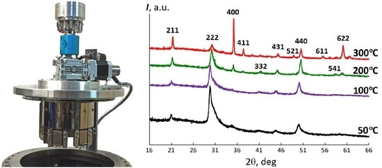
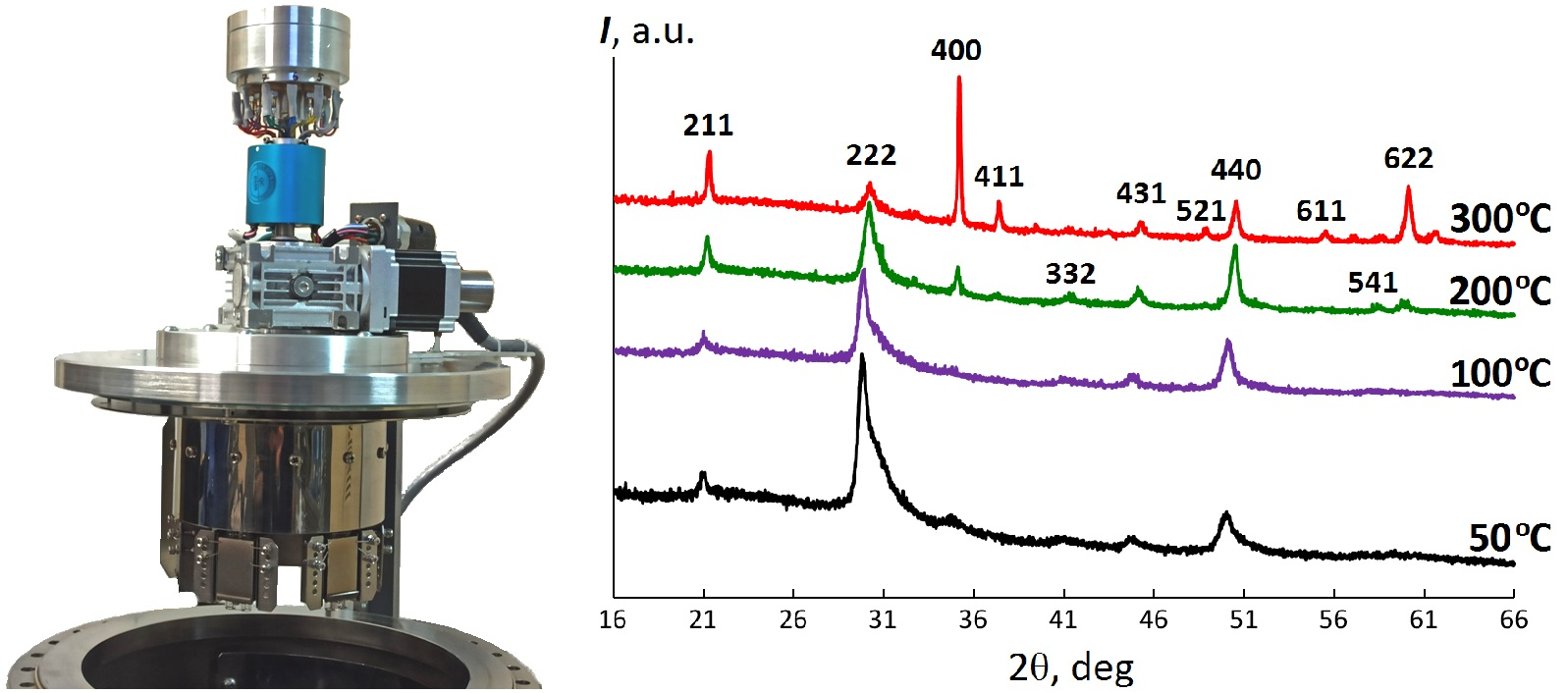
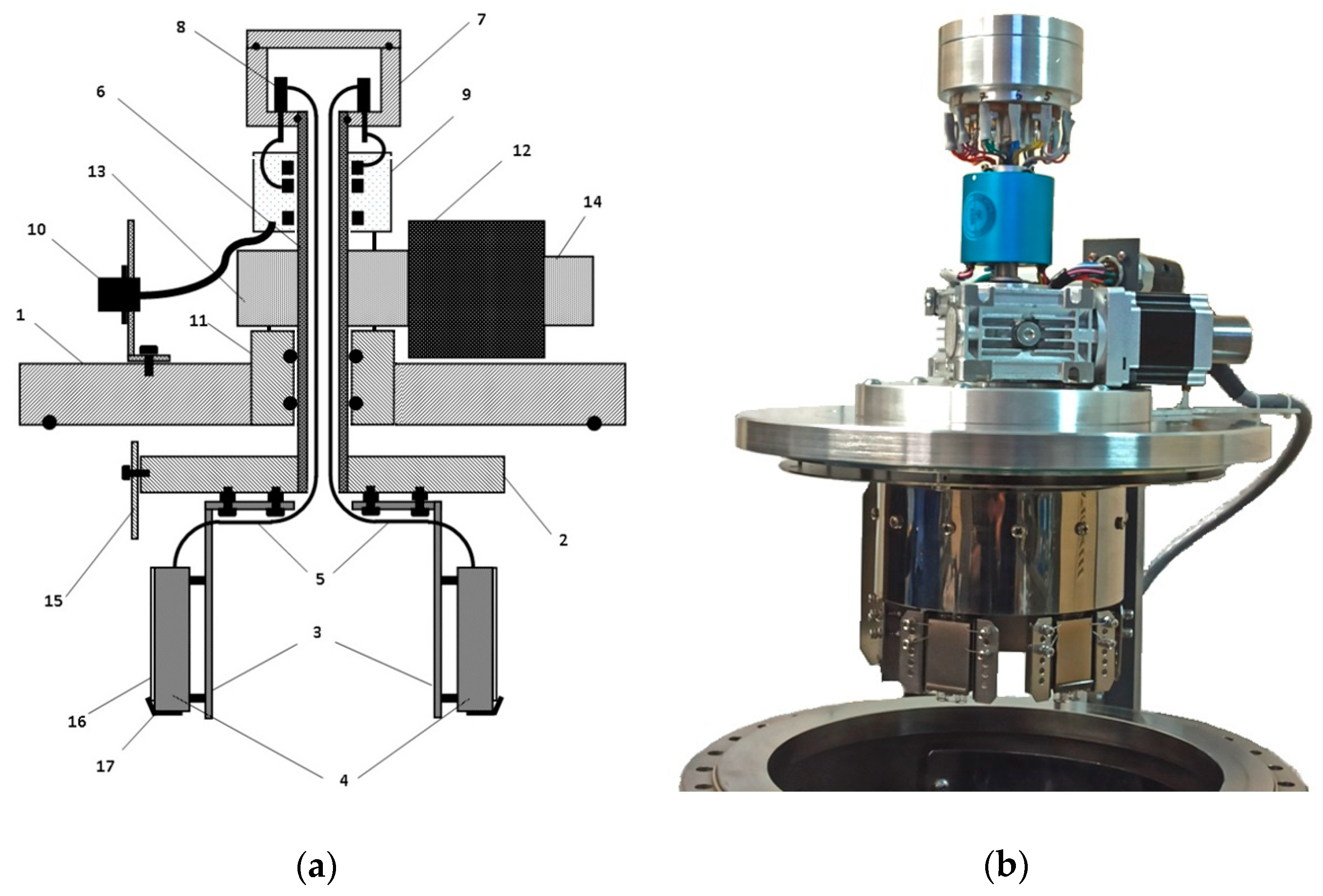
2.1. Description of the Developed MPDTA
2.2. ITO Thin Films Synthesis by Using of the Developed MPDTA
2.3. Film Characterization
3. Results and Discussion
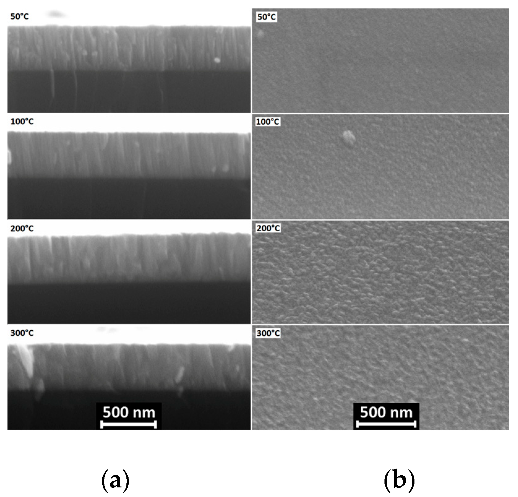
3.1. SEM Analysis
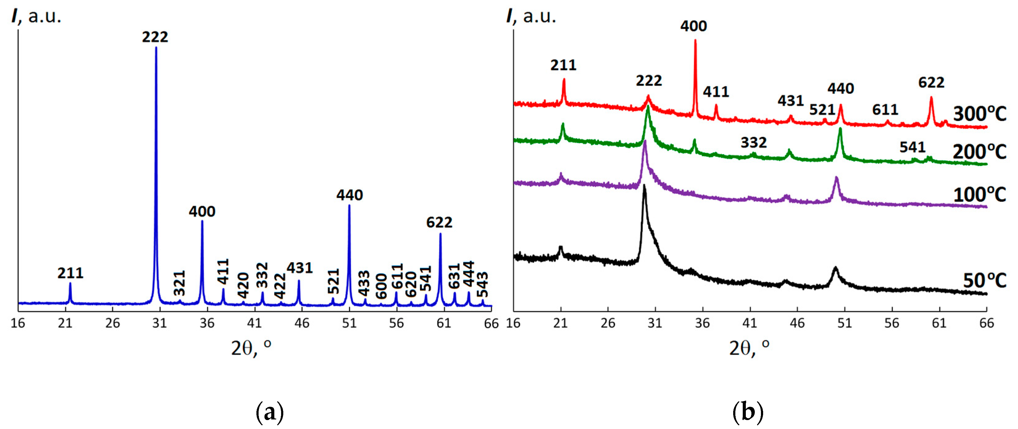
3.2. XRD Analysis
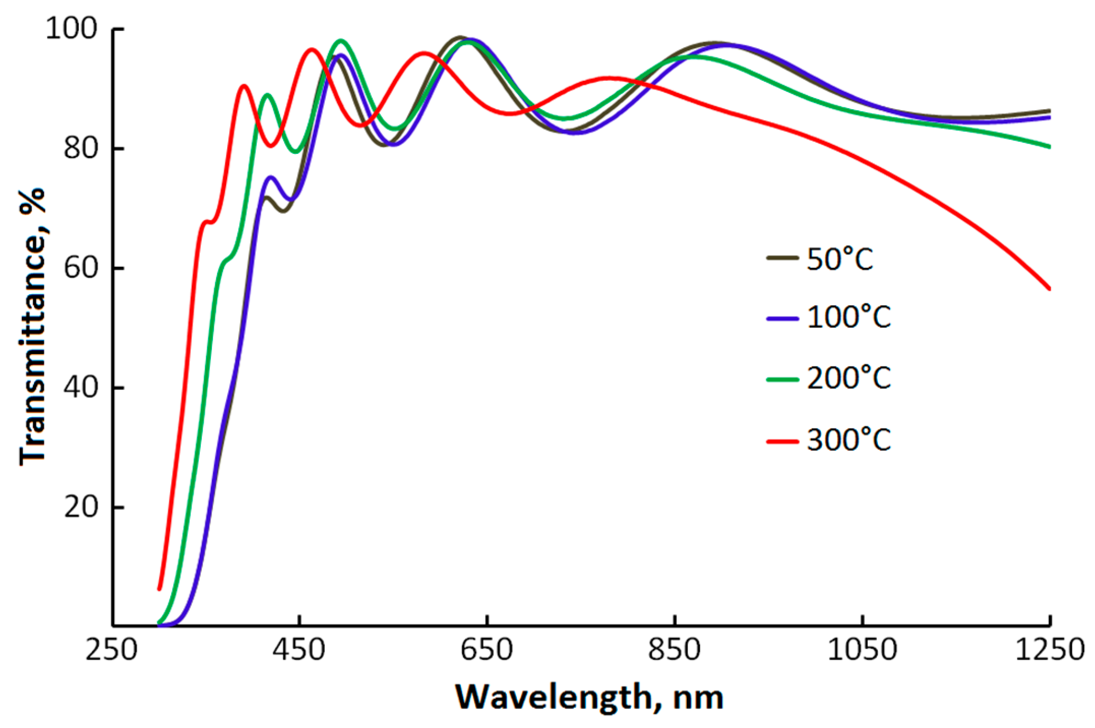
3.3. Functional Performances
4. Conclusions
Supplementary Materials
Author Contributions
Funding
Acknowledgments
Conflicts of Interest
References
- Akhmedov, A.K.; Abduev, A.K.; Kanevsky, V.M.; Muslimov, A.E.; Asvarov, A.S. Low-temperature fabrication of high-performance and stable GZO/Ag/GZO multilayer structures for transparent electrode applications. Coatings 2020, 10, 269. [Google Scholar] [CrossRef] [Green Version]
- Swart, P.L.; Lacquet, B.M.; Reynecke, S. A substrate heater with fast response for a low current ion-implanter. IEEE Trans. Nucl. Sci. 1993, 40, 262. [Google Scholar] [CrossRef]
- Hanak, J.J. The “multiple-sample concept” in materials research: Synthesis, compositional analysis and testing of entire multicomponent systems. J. Mater. Sci. 1970, 5, 964. [Google Scholar] [CrossRef]
- Han, Y.; Siol, S.; Zhang, Q.; Zakutayev, A. Optoelectronic properties of strontium and barium copper sulfides prepared by combinatorial sputtering. Chem. Mater. 2017, 29, 8239. [Google Scholar] [CrossRef]
- Fekete, A.; Jakab-Farkas, L. Practical and low-cost solution for the temperature control of a substrate heater for thin film deposition. In Proceedings of the 2018 International Conference on Development and Application Systems (DAS), Suceava, Romania, 24–26 May 2018. [Google Scholar] [CrossRef]
- Ohkubo, I.; Christen, H.M.; Kalinin, S.V.; Jellison, G.E., Jr.; Rouleau, C.M.; Lowndes, D.H. High-throughput growth temperature optimization of ferroelectric SrxBa1−xNb2O6 epitaxial thin films using a temperature gradient method. Appl. Phys. Lett. 2004, 84, 1350. [Google Scholar] [CrossRef]
- Gregoire, J.M.; van Dover, R.B.; Jin, J.; DiSalvo, F.J.; Abruña, H.D. Getter sputtering system for high-throughput fabrication of composition spreads. Rev. Sci. Instrum. 2007, 78, 072212. [Google Scholar] [CrossRef] [Green Version]
- Tran, D.-P.; Lu, H.-I.; Lin, C.-K. Conductive characteristics of indium tin oxide thin film on polymeric substrate under long-term static deformation. Coatings 2018, 8, 212. [Google Scholar] [CrossRef] [Green Version]
- Deyu, G.K.; Hunka, J.; Roussel, H.; Brötz, J.; Bellet, D.; Klein, A. Electrical properties of low-temperature processed Sn-doped In2O3 thin films: The role of microstructure and oxygen content and the potential of defect modulation doping. Materials 2019, 12, 2232. [Google Scholar] [CrossRef] [Green Version]
- López, M.; Frieiro, J.L.; Nuez-Martínez, M.; Pedemonte, M.; Palacio, F.; Teixidor, F. Nanostructure ITO and get more of it. Better performance at lower cost. Nanomaterials 2020, 10, 1974. [Google Scholar] [CrossRef] [PubMed]
- Joo, S.Y.; Loka, C.; Jo, Y.W.; Reddyprakash, M.; Moon, S.W.; Choi, Y.; Lee, S.E.; Cho, G.S.; Lee, K.-S. ITO/SiO2/ITO structure on a sapphire substrate using the oxidation of ultra-thin si films as an insulating layer for one-glass-solution capacitive touch-screen panels. Coatings 2020, 10, 134. [Google Scholar] [CrossRef] [Green Version]
- Dong, L.; Zhu, G.; Xu, H.; Jiang, X.; Zhang, X.; Zhao, Y.; Yan, D.; Yuan, L.; Yu, A. Fabrication of nanopillar crystalline ITO thin films with high transmittance and IR reflectance by RF magnetron sputtering. Materials 2019, 12, 958. [Google Scholar] [CrossRef] [PubMed] [Green Version]
- Rogozin, A.; Vinnichenko, M.; Shevchenko, N.; Vazquez, L.; Mücklich, A.; Kreissig, U.; Yankov, R.A.; Kolitsch, A.; Möller, W. Effect of elevated substrate temperature on growth, properties, and structure of indium tin oxide films prepared by reactive magnetron sputtering. J. Mater. Res. 2007, 22, 2319. [Google Scholar] [CrossRef]
- Shakiba, M.; Kosarian, A.; Farshidi, E. Effects of processing parameters on crystalline structure and optoelectronic behavior of DC sputtered ITO thin film. J. Mater. Sci. 2017, 28, 787. [Google Scholar] [CrossRef]
- Najwa, S.; Shuhaimi, A.; Talik, N.A.; Ameera, N.; Sobri, M.; Rusop, M. In-situ tuning of Sn doped In2O3 (ITO) films properties by controlling deposition Argon/Oxygen flow. Appl. Surf. Sci. 2019, 479, 1220. [Google Scholar] [CrossRef]
- Zhang, W.; Zhu, G.; Zhi, L.; Yang, H.; Yang, Z.; Yu, A.; Xu, H. Structural, electrical and optical properties of indium tin oxide thin films prepared by RF sputtering using different density ceramic targets. Vacuum 2012, 86, 1045. [Google Scholar] [CrossRef]
- Buscaglia, M.T.; Buscaglia, V.; Viviani, M.; Nanni, P.; Hanuskova, M. Influence of foreign ions on the crystal structure of BaTiO3. J. Eur. Ceram. 2000, 20, 1997. [Google Scholar] [CrossRef]
- Holder, C.F.; Schaak, R.E. Tutorial on powder X-ray diffraction for characterizing nanoscale materials. ACS Nano 2019, 13, 7359. [Google Scholar] [CrossRef] [Green Version]
- Chen, Y.; Zhou, Y.; Zhang, Q.; Zhu, M.; Liu, F. The correlation between preferred orientation and performance of ITO thin films. J. Mater. Sci. 2007, 18, S411. [Google Scholar] [CrossRef]
- Daza, L.G.; Acosta, M.; Castro-Rodriguez, R.; IRIBARREN, A. Tuning optical properties of ITO films grown by rf sputtering: Effects of oblique angle deposition and thermal annealing. Trans. Nonferrous Met. Soc. China 2019, 29, 2566. [Google Scholar] [CrossRef]
- Thirumoorthi, M.; Thomas Joseph Prakash, J. Structure, optical and electrical properties of indium tin oxide ultra thin films prepared by jet nebulizer spray pyrolysis technique. J. Asian Ceram. Soc. 2016, 4, 124. [Google Scholar] [CrossRef] [Green Version]
- Guillén, C.; Herrero, J. Influence of oxygen in the deposition and annealing atmosphere on the characteristics of ITO thin films prepared by sputtering at room temperature. Vacuum 2006, 80, 615. [Google Scholar] [CrossRef]
- Haacke, G. New figure of merit for transparent conductors. J. Appl. Phys. 1976, 47, 4086. [Google Scholar] [CrossRef]
- BIOTAIN CRYSTAL. Available online: http://www.crystal-material.com/Substrate-Materials (accessed on 7 October 2020).
- KINTEC. Available online: http://www.kintec.hk (accessed on 7 October 2020).
- Yang, S.; Zhong, J.; Sun, B.; Zeng, X.; Luo, W.; Zhao, X.; Shu, Y.; Chen, J.; He, J. Influence of base pressure on property of sputtering deposited ITO film. J. Mater. Sci. 2019, 30, 13005. [Google Scholar] [CrossRef]


| Tsub, °C | R□, Ω/sq. | ρ, × 10−4 Ω·cm | Tav, % | ϕ, × 10−3 Ohm−1 |
|---|---|---|---|---|
| 50 | 50.0 ± 0.5 | 20.9 ± 0.4 | 76.0 | 1.25 |
| 100 | 42.0 ± 0.5 | 17.2 ± 0.4 | 75.9 | 1.49 |
| 200 | 8.3 ± 0.1 | 3.4 ± 0.08 | 79.6 | 12.2 |
| 300 | 3.6 + 0.1 | 1.5 ± 0.04 | 80.4 | 30.5 |
Publisher’s Note: MDPI stays neutral with regard to jurisdictional claims in published maps and institutional affiliations. |
© 2020 by the authors. Licensee MDPI, Basel, Switzerland. This article is an open access article distributed under the terms and conditions of the Creative Commons Attribution (CC BY) license (http://creativecommons.org/licenses/by/4.0/).
Share and Cite
Akhmedov, A.K.; Asvarov, A.S.; Muslimov, A.E.; Kanevsky, V.M. A Multi-Position Drum-Type Assembly for Simultaneous Film Deposition at Different Temperatures in a Single Sputter Cycle–Application to ITO Thin Films. Coatings 2020, 10, 1076. https://doi.org/10.3390/coatings10111076
Akhmedov AK, Asvarov AS, Muslimov AE, Kanevsky VM. A Multi-Position Drum-Type Assembly for Simultaneous Film Deposition at Different Temperatures in a Single Sputter Cycle–Application to ITO Thin Films. Coatings. 2020; 10(11):1076. https://doi.org/10.3390/coatings10111076
Chicago/Turabian StyleAkhmedov, Akhmed K., Abil S. Asvarov, Arsen E. Muslimov, and Vladimir M. Kanevsky. 2020. "A Multi-Position Drum-Type Assembly for Simultaneous Film Deposition at Different Temperatures in a Single Sputter Cycle–Application to ITO Thin Films" Coatings 10, no. 11: 1076. https://doi.org/10.3390/coatings10111076