Pure Sn Coatings Produced by Pulse Plating from Stannate Bath


Department of Energy Systems Research and Department of Materials Science and Engineering, Ajou University, Suwon 16499, Korea
*
Authors to whom correspondence should be addressed.
Coatings 2020, 10(2), 117; https://doi.org/10.3390/coatings10020117
Submission received: 7 January 2020
/
Revised: 23 January 2020
/
Accepted: 28 January 2020
/
Published: 30 January 2020
(This article belongs to the Special Issue Coatings and Interfaces)
Abstract
:We have produced pure Sn coatings from an alkaline bath plating. The plating bath was composed of sodium stannate and sodium hydroxide with sorbitol as an additive. The experiments were performed with a potentiostat/galvanostat at various current densities from 5–25 mA/cm2. The morphology of the coatings, thickness, plating rate, and microhardness were evaluated. Furthermore the wetting of the Sn coatings on a Cu substrate was also assessed by area spread ratio measurements after reflow at 250 °C. The resultant coatings were very smooth and shiny. Initially, the plating morphology was uneven and a nodular type, which further improved with increasing current density up to 15 mA/cm2. The plating rate and thickness were the maximum at a current density of 15 mA/cm2. The coatings had higher strength and solderability at 15 mA/cm2 due to the improved microstructure and plating rate.
1. Introduction
Microelectronic circuits are very sensitive to the formation of unwanted metallic outgrowths over time. These metallic outgrowths are termed as whiskers, which originate due to high residual stresses inside the coatings. These whiskers can cause short-circuiting of electronic circuits if not controlled properly [1,2]. Therefore, the protection of electronic components is of utmost importance. There are various factors that influence the presence of these whiskers. The prime factor is the build-up of stresses in the deposits due to the non-uniform chemistry of the deposits, external environment and corrosive factors [3]. The coating techniques such as vapor deposition, evaporation, sol–gel, or laser deposition require expensive tooling and great control during the experiment. Among various methods, electrochemical plating is the most economical and simplest method for the surface protection of electronic conductors [4]. In acidic bath plating, various kinds of complex chemical formulations are used to alleviate the deposit stress. However, the addition of many chemicals to plating baths causes poor stability, chemical degradation, and/or whiskering over time [5,6]. Acidic baths are more popular due to their important role in high-quality surface finish, but require sophisticated disposal systems [7,8,9,10,11].
In contrast, alkaline baths are eco-friendly and rarely need additional organic chemicals for deposition. However, there is a scarcity of literature data about alkaline plated metallic systems, especially pure Sn [12,13]. Sharma et al. studied additive-free alkaline tin plating and found that whiskers were generated after the storage of tin coatings for one year. It was found that current density played an important role in controlling the orientation of deposits and whisker growth [13]. In another study, a comparison of tin-plated coatings was made from different plating baths, however, the deposit efficiency of the alkaline bath was inferior to that of acidic baths [1]. In addition, it has been noted by earlier researchers that alkaline tin plating generates minimum stress in deposits, which may be beneficial for the minimization of tin whisker growth [13,14]. Finnazi et al. developed an alkaline tin–copper bath using sorbitol and found an enhancement in the plating microstructure and quality [12]. It can be inferred that there exists a possibility to explore the alkaline baths for the tin plating of electronic components. Pure tin is also a choice for electronics manufacturers for non-toxic and lead-free surface finishes in microelectronic applications. In addition, a pure Sn finish is a lot cheaper option than a common Sn–Ag or Sn–Ag–Cu solder finish.
Therefore, in the present work, we attempted to deposit pure Sn by pulse plating from an alkaline bath. Compared to previous studies, this study employed a safe cyanide-free electrolyte for tin plating [12,13,14]. In addition, we used pulse plating for a better surface finish and quality control [4,5,6]. In pulse plating, a current pulse wave is applied for a given time and stopped for a certain duration, and this cycle is repeated [4]. This type of switching (on and off) the pulse reduces the thickness of the diffusion layer and allows more ions to deposit onto the cathode, which increases the deposition rate compared to the conventional direct current plating [4,5,6,13].
While most studies have focused only on microstructure and whisker growth, in this study, we evaluated the wetting of the deposits as a function of current density. Wetting of the tin finish is crucial for the soldering of copper conductors in electronics assemblies. Furthermore, the role of current density on the microstructure, plating rate, and thickness was also studied.
2. Materials and Methods
The plating bath composition and parameters are shown in Table 1. Sorbitol is used as an additive that provides a higher deposition rate, improves the surface finish, minimizes the porosity, and stabilizes the bath [12]. An alkaline bath was chosen for its non-toxic and environmentally safe properties in comparison to commercial cyanide-based and multi-component acidic baths. The chemicals (≈99.8% purity) were purchased from Sigma Aldrich, USA. The bath chemicals, as shown in Table 1, were dissolved in deionized water. This solution was further stirred overnight at 300 rpm.
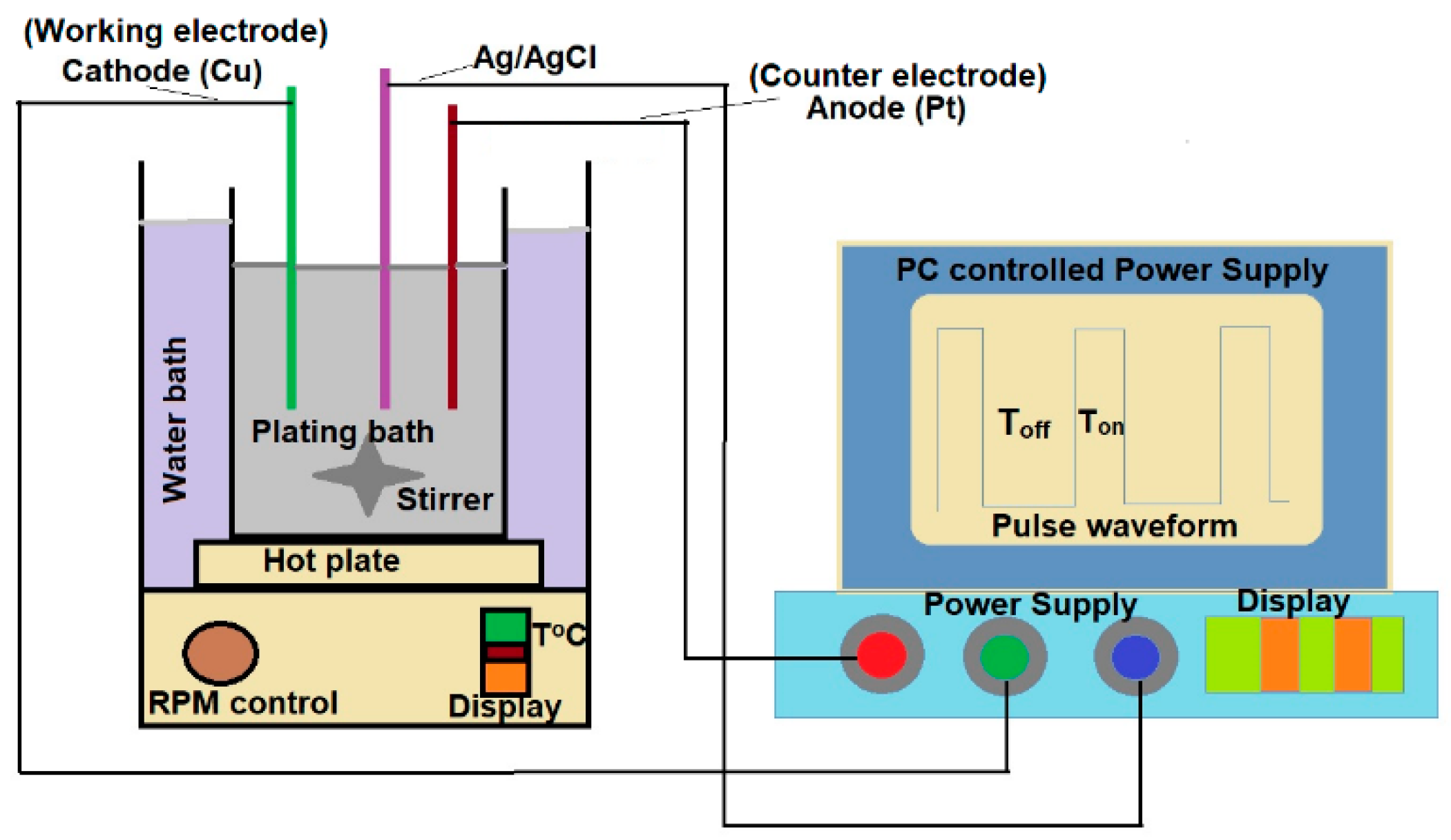
A three-electrode geometry cell was chosen that consisted of a Cu plate as a working electrode (0.3 mm × 0.1 mm × 0.1 mm), a platinum wire as the counter electrode, and a Ag/AgCl (3KCl) electrode as a reference. Prior to the experiment, the Cu cathode was rinsed in 10% dilute H2SO4, followed by alcohol drying to remove the dirt and oxides.
The plating was done using a potentiostat/galvanostat (EPP-4000, EC-LAB, Biologic, France). The plating bath was heated at a temperature of 43 °C with all electrodes immersed in it with stirring continuously at 300 rpm. We found that alkaline baths produce a spongy deposit at room temperature, and that the deposit quality improves at elevated temperatures. After trial experiments, we fixed the temperature of 43 °C for our plating experiments. The duration was chosen to have a considerable thickness for the characterization studies. The employed parameters are shown in Table 2.
The pulse current was applied during the experiment (Figure 1). The characterization studies were performed using scanning electron microscopy (SEM, JEOL 7000F, JEOL Ltd., Tokyo, Japan), and a benchtop Miniflex 300 x-ray diffractometer (XRD, Rigaku Corporation, Tokyo, Japan) operating at 35 kV, 35 mA, and λcopper ≈ 1.54 Å. The coatings were checked for their composition by energy dispersive spectroscope (EDS) coupled to the SEM.
After the characterization studies, the thickness and plating rate of the deposits were measured after weighing the coatings by a high precision (least count ≈ 0.1 mg) weighing machine (Sartorius, BSA-224S-CW, Sartorius Lab Instruments GmbH, Goettingen, Germany).
The microhardness test on the coatings was performed with an automated Vickers hardness tester (Mitutoyo HM-210, Kanagawa, Japan). The loading force and time were 25 g and 20 s, respectively. Five sets of measurements were taken and averaged out for the maximum accuracy of the obtained microhardness value.
The wetting of the coatings was studied by the spreading ratio method. The coatings were reflowed at 250 °C, and the difference in the areas of the coatings before and after reflow was recorded.
3. Results
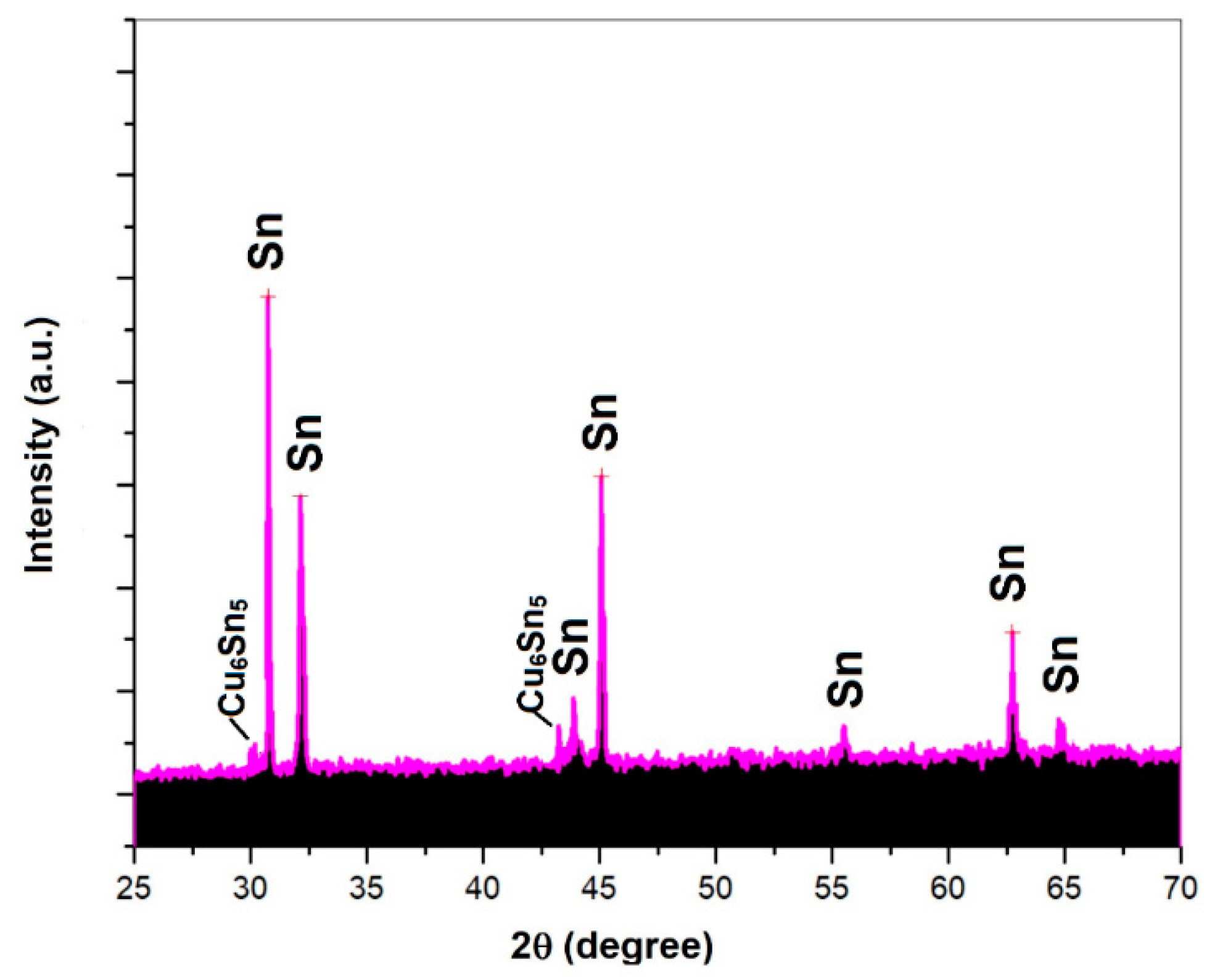
3.1. XRD
The phase structural analysis of the pure Sn plated from alkaline baths is shown in Figure 2. The various peaks in the XRD spectrum were matched with the JCPDS file 04-0673 (for β-Sn) and 45-1488 (for Cu6Sn5). There were numerous peaks related to β-Sn while a tiny peak was also found that belonged to Cu6Sn5 intermetallic compounds (IMCs), which may come from the adherent substrate [13,14,15,16].
IMCs form while plating due to the fact that Cu atoms diffuse at the grain boundaries and precipitate out. All samples showed a similar structure deposited from various current densities, which is consistent with a number of research reports [16].
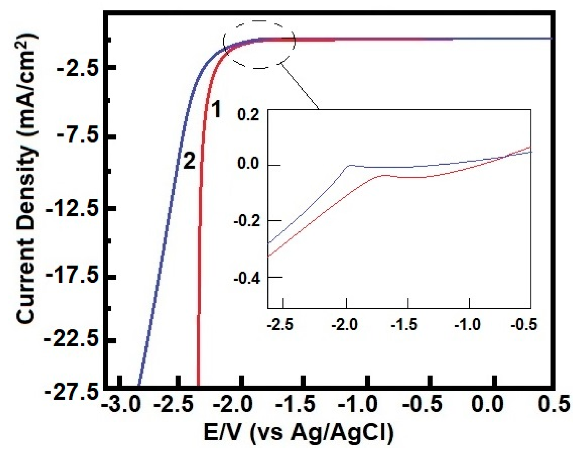
3.2. Polarization
Polarization tests were performed to determine the extent of polarizing behavior and deposition in the respective bath compositions.
Here, (curve 1) is related to sodium stannate and hydroxide. Curve 2 is related to the sodium stannate, sodium hydroxide, and sorbitol (Figure 3). We can see that the reduction potential of Sn lies at −1.85 V, and after that, the current density increases rapidly with potential (curve 1). The curve shifts to the more negative side when sorbitol is added to the bath (curve 2), and the reduction potential changes to −1.96 V following hydrogen evolution. The hydrogen evolution was depressed a bit in this case. The shifting of potential to a negative side points toward the increased cathodic polarization of the electrode, which indicates an improved deposition rate [17]. The chronopotentiometry curves recorded in the electrolyte (Na2SnO3 + NaOH + sorbitol) at 15 and 25 mA/cm2 are shown in Supplementary Figure S1. The potential decreased initially due to the charging of the double layer and the reduction reaction at the cathode until the concentration of ([Sn(OH)6]2−) at the cathode became zero. In contrast, at a current density of 25 mA/cm2, the potential dropped quickly, signaling a rapid hydrogen evolution reaction compared to metal deposition. This indicates a synergistic behavior of NaOH and sorbitol in the plating bath, which is beneficial for uniform deposition and morphology. The reduction of Sn ions occurred around −1.8 V from the tin hydroxyl complex ([Sn(OH)6]2−) and parallel hydrogen evolution occurred beyond −2.3 V [18].
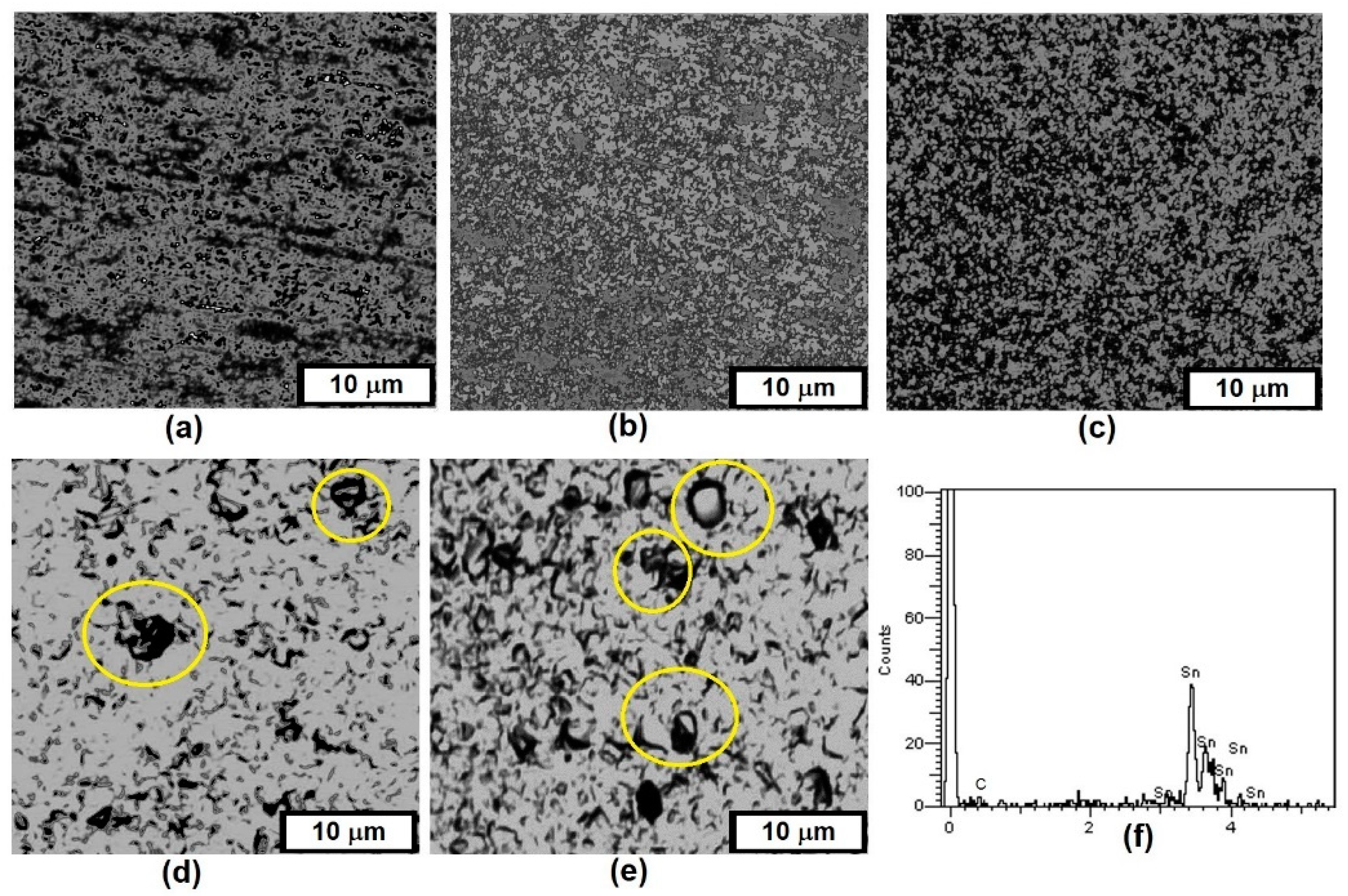
3.3. Morphology
The coating morphology at various current densities is shown in Figure 4. The SEM images show an irregular surface due to uneven cathode coverage at 5 mA/cm2. The morphology turns smooth at moderately higher current densities (i.e., 10–15 mA/cm2) due to a higher deposition rate. Additionally, the smoothness was the highest for the deposit plated at 10 mA/cm2. Qualitatively, the smoothness is influenced by the morphology and roughness of the underlying copper substrate. In general, a rough surface is more prone to the formation of IMCs (Cu6Sn5, Cu3Sn) due to higher surface energy and Cu–Sn diffusion across the interface. The formation of the IMCs leads to uneven surface areas where Sn grains can be accumulated preferentially. This type of non-uniformity in surface increases at higher current densities due to a higher density of ad-atoms and deposition rate. At very high current densities (i.e., 20–25 mA/cm2), the development of the pores was also noticed, which led to a fall in deposition rate and non-uniform, porous, and irregular deposits [19,20].
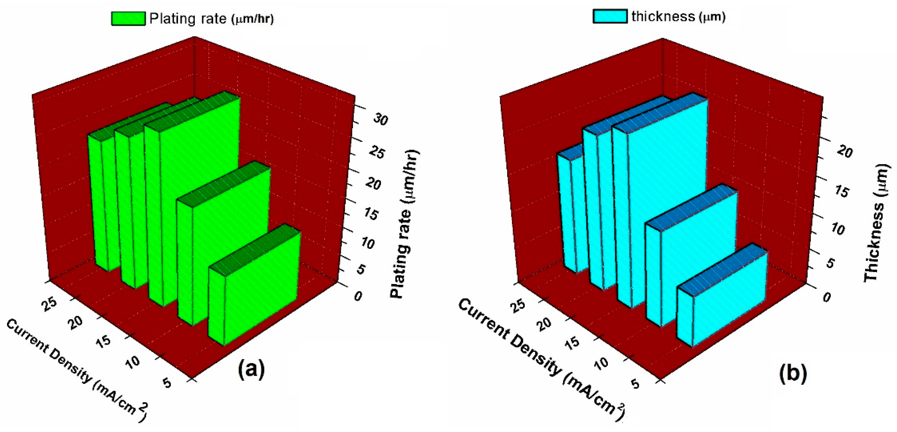
3.4. Deposition Rate
The deposition rate as a function of current density is shown in (Figure 5a). The coating thickness was also plotted in Figure 5b. The typical mass of the deposits was of the order of 0.062–0.120 g. The plating rate rises initially with current density. This can be due to the increased flow of electrons available for the reduction of ([Sn(OH)6]2−) ions. Furthermore, the deposition rate reduces after achieving maximum value at 15 mA/cm2. The thickness of the deposits also follows a similar trend with increasing current densities. The maximum plating rate was 18–27 μm/h at 15 mA/cm2. The maximum thickness was 32 μm.
The plating rate decreases at higher current densities beyond 15 mA/cm2 due to the increased hydrogen evolution. As a consequence, the coating mass is also decreased and the morphology turns very poor. More precisely, the plating rate (θ) can be defined from the relation of coating mass (mexperimental), thickness (d), and cathodic current efficiency (η) as follows:
where t is the plating time; M is the molecular mass; Z is the number of electrons; F is Faraday’s constant; ρ is the metal density; and J is the plating current density (current flow per unit area = I/A). The current efficiency (η) is related by the ratio of the experimental mass of coatings to that of the theoretical mass derived from Faraday’s law of electrolysis.
J = I/A
The current efficiency (η) is presented in Table 3. It can be seen that η reaches a maximum value at a current density of 15 mA/cm2 and decreases thereafter.
From Equations, (1)–(4), it can be seen that for a high θ or η, the J cannot be increased indefinitely due to the limiting mass transport across the electrolyte–cathode interface. The limiting current density is given by:
where Di is the diffusion coefficient of the metal ions (cm2/s); δ is the thickness of the diffusion layer over the cathode and bulk of the electrolyte medium. When J >> Jlim, (>> 15 mA/cm2), the supply of metal ions becomes limited across the cathode–electrolyte interface. To compensate for the metal discharge process, hydrogen evolution becomes a dominant reaction. A high current density results in burnt-out, porous deposits due to the limited metal ions at the cathode interface. The hydrogen ions reduce to hydrogen gas and make the surface highly porous and uneven. All these combined processes make the plating rate very poor.
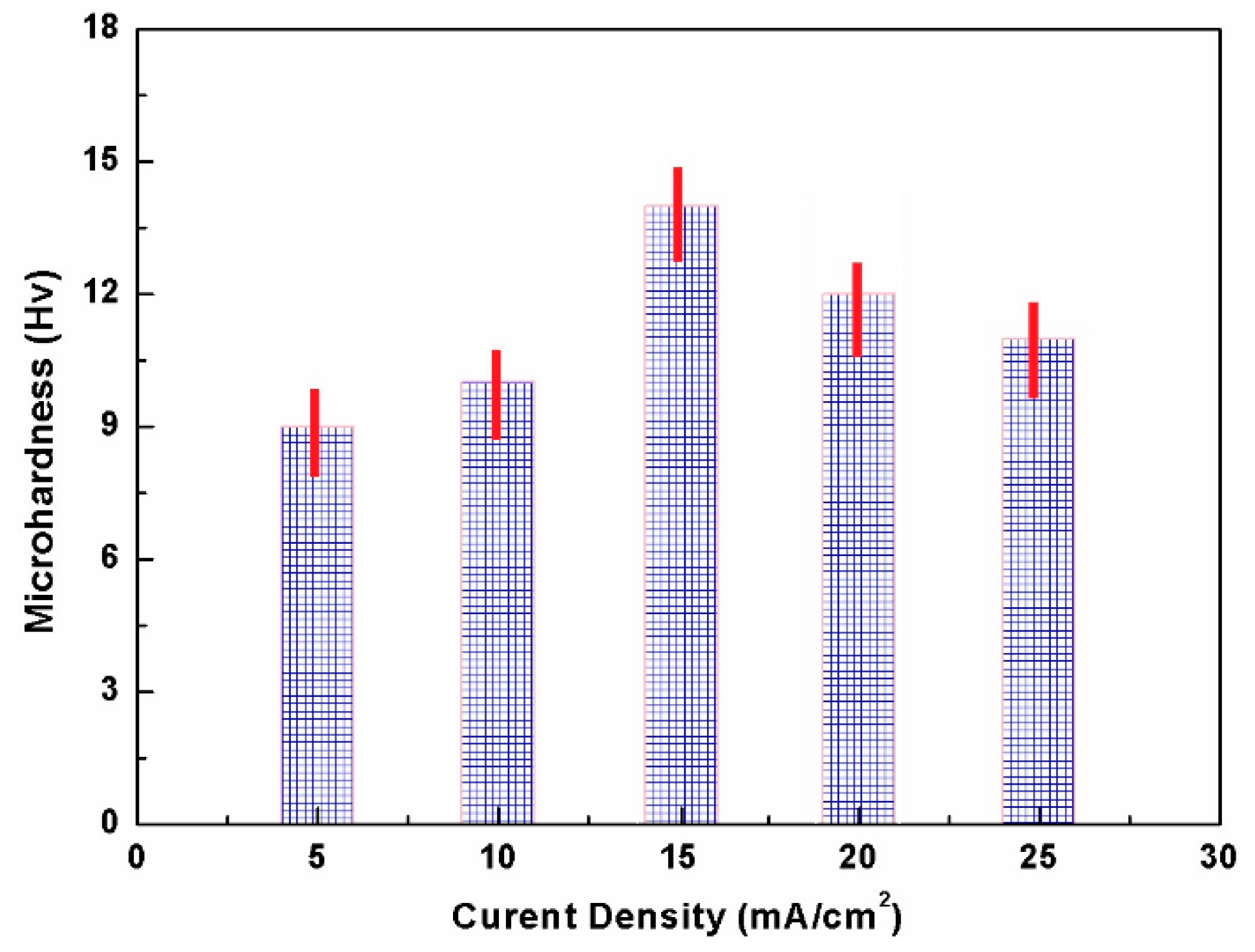
3.5. Microhardness
The mechanical properties of the coatings were also evaluated with a Vickers hardness tester as shown in Figure 6. The microhardness of the deposits rises from 9 to 14 Hv, up to a current density of 15 mA/cm2.
The increase in microhardness can be due to the refinement of grains in the coatings. However, a decrease in microhardness beyond 15 mA/cm2 was also noticed, which supported the presence of pores and reduced metal deposition. As a consequence, the microhardness of coatings decreased beyond 15 mA/cm2 [9,19,20,21].
3.6. Solderability
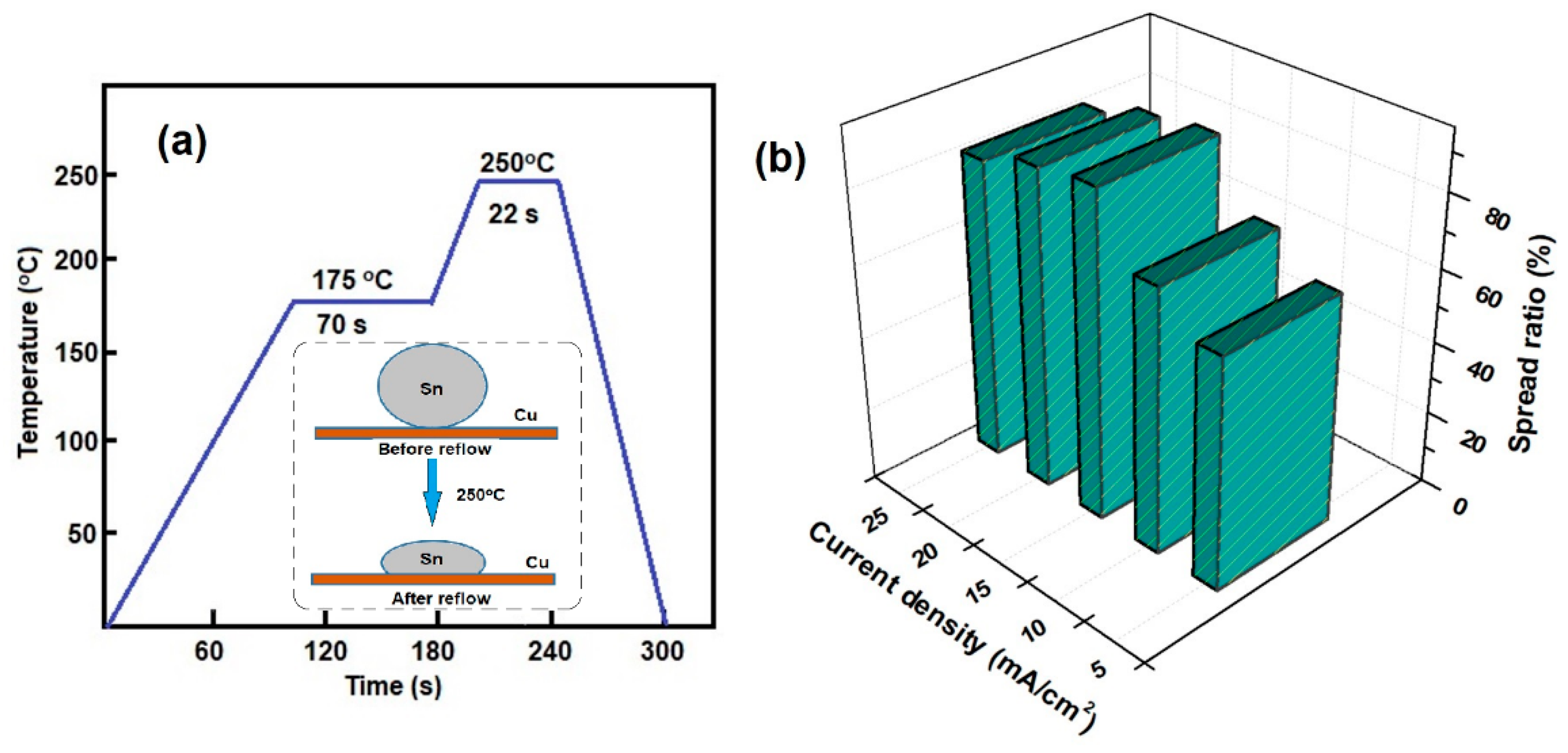
The solderability of the coatings after reflow at 250 °C is shown in Figure 7a,b. The reflow process consists of (a) attaching the metal deposit on Cu conductors, (b) controlled heating of the whole assembly up to a reflow temperature, and (c) melting and solidification of the metal. The metal melts and flows out over the conducting surface. The wetting can be approximated in terms of the change in area percentage before and after the reflow process. The reflow process is shown schematically in the inset of Figure 7a. Initially, the wetting improved with the current density. The reason is ascribed to the enhanced deposition rate, which improves the fluidity of the melt. However, there was no appreciable change beyond the current density of 15 mA/cm2.
At higher current densities, the spread ratio is not affected severely because of the presence of pores in the deposits [22]. The spread ratio is affected by the deposition rate, which depends upon the current density. In other words, we can optimize the current density to obtain a good and solderable tin finish on metal conductors.
4. Conclusions
In this work, we produced Sn coatings by the pulse electrodeposition method. We used an alkaline stannate bath for the plating experiments. The plated films were composed of a β-Sn tetragonal crystal structure. In addition, a small amount of Cu6Sn5 IMCs also formed with the β-Sn phase. It was found that an increase in the current density led to the refinement of the grains in the coating of up to 15 mA/cm2. However, a further rise in current density raised the porosity levels in the deposits due to the incorporation of hydrogen gases in the deposits. The thickness, deposition, and current efficiency rate were the maximum at 15 mA/cm2. The microhardness and spreadability of the coatings were also maximum at 15 mA/cm2 due to the higher deposition rate and improved melt fluidity. The obtained thin layers can be used as a solderable coating for improvement in the wetting of metal substrates in joining, and the surface protection of electronic components in microelectronic packaging and circuits.
Supplementary Materials
The following are available online at https://www.mdpi.com/2079-6412/10/2/117/s1, Figure S1: The chronopotentiometry curves of Sn recorded in Na2SnO3 + NaOH + sorbitol electrolyte.
Author Contributions
B.A. provided the concept and facility for carrying out this work. H.S. acquired the financial support for this publication. A.S. performed the experiments, methodology, and prepared the original draft of this manuscript. A.S. analyzed the data and provided the mechanism of the plating. B.A. and H.S. reviewed the draft and recommended final corrections. All authors have read and agreed to the published version of the manuscript.
Funding
This work was supported by the Ajou University Research Fund.
Conflicts of Interest
The authors declare no conflicts of interest.
References
- Sharma, A.; Das, S.; Das, K. Effect of different electrolytes on the microstructure, corrosion and whisker growth of pulse plated tin coatings. Microelectron. Eng. 2017, 170, 59–68. [Google Scholar] [CrossRef]
- Osenbach, J.W.; DeLucca, J.M.; Potteiger, B.D.; Amin, A.; Baiocchi, F.A. Sn-whiskers: Truths and myths. In Lead-Free Electronic Solders; Springer: Boston, MA, USA, 2006. [Google Scholar]
- Hektor, J.; Marijon, J.B.; Ristinmaa, M.; Hall, S.A.; Hallberg, H.; Iyengar, S.; Micha, J.S.; Robach, O.; Grennerat, F.; Castelnau, O. Evidence of 3D strain gradients associated with tin whisker growth. Scr. Mater. 2018, 144, 1–4. [Google Scholar] [CrossRef]
- Paunovic, M.; Schlesinger, M. Fundamentals of Electrochemical Deposition; Wiley Interscience: New York, NY, USA, 2006. [Google Scholar]
- Sharma, A.; Das, S.; Das, K. Pulse electrodeposition of lead-free tin-based composites for microelectronic packaging. In Electrodeposition of Composite Materials; Mohamed, A.M.A., Golden, T.D., Eds.; InTech: Rijeka, Croatia, 2016; pp. 253–274. [Google Scholar] [CrossRef] [Green Version]
- Sharma, A.; Das, S.; Das, K. Pulse electroplating of ultrafine grained tin coating. In Electroplating of Nanostructures; Mahmood, A., Ed.; Intech: Rijeka, Croatia, 2015; pp. 105–129. [Google Scholar] [CrossRef] [Green Version]
- Carlos, I.A.; Bidoia, E.D.; Pallone, E.M.J.A.; Almeida, M.R.H.; Souza, C.A.C. Effect of tartrate content on aging and deposition condition of copper-tin electrodeposits from a non-cyanide acid bath. Surf. Coat. Technol. 2002, 157, 14–18. [Google Scholar] [CrossRef]
- Dischee, C.A.; Mathers, F.C. Brightening agents for the Tin-II sulfate-sulfuric acid electrolyte. J. Electrochem. Soc. 1955, 102, 387–389. [Google Scholar] [CrossRef]
- Sharma, A.; Jang, Y.J.; Jung, J.P. Effect of current density on morphology of electroplated tin. Surf. Eng. 2015, 31, 458–464. [Google Scholar] [CrossRef]
- Radovic, D. Lead-tin alloy plating with hydroquinone as an additive in fluoborate baths. Plat. Surf. Finish. 1989, 76, 52. [Google Scholar]
- Balaji, R.; Pushpavanam, M. Methanesulphonic acid in electroplating related metal finishing industries. Trans. Inst. Met. Finish. 2003, 81, 154–158. [Google Scholar] [CrossRef]
- Finazzi, G.A.; Oliveira, E.M.D.; Carlos, I.A. Development of a sorbitol alkaline Cu-Sn plating bath and chemical, physical and morphological characterization of Cu-Sn films. Surf. Coat. Technol. 2004, 187, 377–387. [Google Scholar] [CrossRef]
- Sharma, A.; Bhattacharya, S.; Sen, R.; Reddy, B.S.B.; Fecht, H.J.; Das, K.; Das, S. Influence of current density on microstructure of pulse electrodeposited tin coatings. Mater. Charact. 2012, 68, 22–32. [Google Scholar] [CrossRef]
- Ashworth, M.; Wilcox, G.; Higginson, R.; Heath, R.; Liu, C.; Mortimer, R. The effect of electroplating parameters and substrate material on tin whisker formation. Microelectron. Reliab. 2015, 55, 180–191. [Google Scholar] [CrossRef] [Green Version]
- Gaylon, G.T. Annoted Tin Whisker Bibliography and Anthology; NEMI Tin Whisker Modeling Project, NEMI: New York, NY, USA, 2003; pp. 1–64. [Google Scholar]
- Pewnim, N.; Roy, S. Electrodeposition of tin-rich Cu–Sn alloys from a methanesulfonic acid electrolyte. Electrochim. Acta 2013, 90, 498–506. [Google Scholar] [CrossRef]
- Sharma, A.; Bhattacharya, S.; Das, S.; Das, K. A study on the effect of pulse electrodeposition parameters on the morphology of pure tin coatings. Metall. Mater. Trans. A 2014, 45, 4610–4622. [Google Scholar] [CrossRef]
- Popov, K.I.; Zivkovic, P.M.; Jokic, B.; Nikolic, N.D. The shape of the polarization curve and diagnostic criteria for control of the metal electrodeposition process. J. Serb. Chem. Soc. 2016, 81, 291–306. [Google Scholar] [CrossRef] [Green Version]
- Sharma, A.; Bhattacharya, S.; Das, S.; Das, K. Influence of current density on surface morphology and properties of pulse plated tin films from citrate electrolyte. Appl. Surf. Sci. 2014, 290, 373–380. [Google Scholar] [CrossRef]
- Jung, D.H.; Sharma, A.; Kim, K.H.; Choo, Y.C.; Jung, J.P. Effect of current density and plating time on Cu electroplating in TSV and low alpha solder bumping. J. Mater. Eng. Perform. 2015, 24, 1107–1115. [Google Scholar] [CrossRef]
- Sharma, A.; Bhattacharya, S.; Das, S.; Das, K. Fabrication of Sn-Ag/CeO2 electro-composite solder by pulse electrodeposition. Metall. Mater. Trans. A 2013, 44, 5587–5601. [Google Scholar] [CrossRef]
- Sharma, A.; Chung, C.-H.; Ahn, B. Pulse co-deposition of tin-silver alloy from citric acid plating bath for microelectronic applications. Mater. Res. Express 2019, 6, 1165g8. [Google Scholar] [CrossRef]
Figure 1.
Pulse plating setup used for the experiment.

Figure 2.
XRD pattern of the tin-plated coating.

Figure 3.
Cathodic polarization curve obtained from the various baths (1) Na2SnO3.3H2O + NaOH, and (2) NaOH + Na2SnO3.3H2O + C6H14O6. The inset shows the magnified view.
Figure 3.
Cathodic polarization curve obtained from the various baths (1) Na2SnO3.3H2O + NaOH, and (2) NaOH + Na2SnO3.3H2O + C6H14O6. The inset shows the magnified view.

Figure 4.
SEM images of the tin plated at various current densities. (a) 5, (b) 10, (c) 15, (d) 20, and (e) 25 mA/cm2. The compositional analysis of deposits (c) is shown in (f).
Figure 4.
SEM images of the tin plated at various current densities. (a) 5, (b) 10, (c) 15, (d) 20, and (e) 25 mA/cm2. The compositional analysis of deposits (c) is shown in (f).

Figure 5.
(a) Plating rate and (b) thickness of the tin coatings as a function of current density.

Figure 6.
Microhardness of the tin coatings as a function of current density.

Figure 7.
(a) Reflow profile and (b) solderability of the Sn coatings at different current density. The square with broken lines shows the schematic of the reflow process.
Figure 7.
(a) Reflow profile and (b) solderability of the Sn coatings at different current density. The square with broken lines shows the schematic of the reflow process.


Table 1.
Bath chemicals.
| Components | Amount |
|---|---|
| Sodium stannate (Na2SnO3.3H2O) | 0.30 mol/L |
| Sodium hydroxide (NaOH) | 0.40 mol/L |
| Sorbitol (C6H14O6) | 0.25 mol/L |
Table 2.
Bath Parameters.
| Bath Parameters | Values |
|---|---|
| pH | 13 |
| Current Density | 5–25 mA/cm2 |
| Bath Temperature | 44–50 °C |
| Duration | 30 min |
| Agitation | 300 rpm |
| Pulse time | 0.001 s, 0.01 s |
| Duty Cycle (%) | 9% |
| Frequency (Hz) | 90 |
Table 3.
Cathodic current efficiency (η) at various current densities (J).
| J (mA/cm2) | η (%) |
|---|---|
| 5 | 55 |
| 10 | 68 |
| 15 | 79 |
| 20 | 71 |
| 25 | 63 |
© 2020 by the authors. Licensee MDPI, Basel, Switzerland. This article is an open access article distributed under the terms and conditions of the Creative Commons Attribution (CC BY) license (http://creativecommons.org/licenses/by/4.0/).
Share and Cite
MDPI and ACS Style
Sharma, A.; Seo, H.; Ahn, B. Pure Sn Coatings Produced by Pulse Plating from Stannate Bath. Coatings 2020, 10, 117. https://doi.org/10.3390/coatings10020117
AMA Style
Sharma A, Seo H, Ahn B. Pure Sn Coatings Produced by Pulse Plating from Stannate Bath. Coatings. 2020; 10(2):117. https://doi.org/10.3390/coatings10020117
Chicago/Turabian StyleSharma, Ashutosh, Hyungtak Seo, and Byungmin Ahn. 2020. "Pure Sn Coatings Produced by Pulse Plating from Stannate Bath" Coatings 10, no. 2: 117. https://doi.org/10.3390/coatings10020117
Note that from the first issue of 2016, this journal uses article numbers instead of page numbers. See further details here.