Article

Fabrication and Characterization of Hybrid and Tunable ZnO@Ag Flexible Thin Films Used as SERS Substrates

by
Ioana Andreea Brezeștean
1,
Daniel Marconi
1,
Nicoleta Elena Dina
1,
Maria Suciu
2,3,* and
Alia Colniță
1,*
1
Department of Molecular and Biomolecular Physics, National Institute for Research and Development of Isotopic and Molecular Technologies, 67-103 Donat, 400293 Cluj-Napoca, Romania
2
Electron Microscopy Centre “C. Crăciun”, Faculty of Biology and Geology, Babeș-Bolyai University, 5-7 Clinicilor, 400006 Cluj-Napoca, Romania
3
Electron Microscopy Integrated Laboratory LIME-CETATEA, National Institute for Research and Development of Isotopic and Molecular Technologies, 67-103 Donat, 400293 Cluj-Napoca, Romania
*
Authors to whom correspondence should be addressed.
Chemosensors 2023, 11(8), 441; https://doi.org/10.3390/chemosensors11080441
Submission received: 16 June 2023 / Revised: 3 August 2023 / Accepted: 5 August 2023 / Published: 7 August 2023
(This article belongs to the Special Issue Recent Developments in Platforms for SERS Applications)

Abstract

:
Flexible substrates have known increased popularity over rigid ones due to their use in surface-enhanced Raman scattering (SERS). They provide irregular surfaces, ideal for in situ sensing. In this context, we report the SERS performance of hybrid ZnO@Ag thin films deposited by magnetron sputtering (MS) on flexible, thermoplastic substrates. This physical deposition method is acknowledged for obtaining high-quality and reproducible ZnO films that can be embedded in (bio)sensing devices with various applications. Three types of thermoplastic-based, commercially available substrates with different glass transition temperatures (Tg) were chosen for the variation in flexibility, transparency, and thickness. Zeonor® (Tg = 136 °C, thickness of 188 μm) and two types of Topas (Topas®: Tg = 142 °C, thickness of 176 μm; Topas2: Tg = 78 °C, thickness of 140 μm) thermoplastic sheets are nonpolar and amorphous cyclo-olefin polymer (COP) and cyclo-olefin copolymers (COC), respectively. Their thicknesses and different values of Tg can greatly affect the topographical and roughness properties of films with small thicknesses and, thus, can greatly influence the enhancement of the Raman signal. The ZnO films deposited on top of Zeonor® or Topas® have identical morphological properties, as shown by the scanning electron microscopy (SEM) characterization. Subsequently, by using the MS technique, we tuned the thickness of the deposited silver (Ag) films in the range of 7–30 nm to assess the growth influence on the morphology and the SERS signal amplification of the substrates with and without the ZnO intermediate layer. The SEM analysis showed that the Ag atoms migrated both into the interstitial areas, filling the voids between the ZnO granular structures, and over the latter, forming, in this case, isolated Ag clusters. SERS analysis performed on the ZnO-Ag hybrid films using crystal violet (CV) molecule revealed a limit of detection (LOD) of 10−7 M in the case of 15 nm thick Ag/Zeonor® interlayer films ZnO and relative standard deviation (RSD) below 10%.

1. Introduction

Since the dawn of automated technologies, micro/nano-fabricated, portable, and ready-to-integrate thin films have superseded conventional interlayering techniques of hybrid materials with boosted properties [1]. Moreover, there is a constant need for new surface-enhanced Raman scattering (SERS) substrates with exceptional plasmonic enhancement/signal processing, strong plasmonic hot spots, and relatively cheap, easy to fabricate, which can yield reproducible results [2,3,4,5]. Nanostructured and flexible surfaces have great potential for manufacturing anti-counterfeit labels [6], self-color-changing films [7], nanoscale 3D holographic color prints with enhanced optical properties [8], specifically security-customized, or highly sensitive SERS detection platforms [9,10].
SERS is a versatile sensing technique due to the simple, economical, and promising substrates successfully tested in various circumstances: Food safety, security, healthcare, forensics, etc. The plasmonic properties of the substrate can be greatly boosted by tuning the localized surface plasmon resonance (LSPR), responsible for the electromagnetic enhancement in the SERS effect. It is still challenging to obtain substrates with high and reproducible signal enhancement so that analytical applications involving SERS substrates become translated into clinical premises, security checking areas, or food chain supply and control. In particular, the fabrication technologies that offer great uniformity and excellent figures of merit for sensing use are usually elaborate and costly. On the other hand, facile and affordable SERS-based approaches are only tested in a limited context, with no consistency outside the same lab premises.
Among the flexible SERS substrates, the polymeric-based ones have become very popular in various fields: Food safety or animal farming to trace pesticides, fungicides, illegal additives, antibiotics, and foodborne pathogens [9,10], fast and enhanced chemical mapping [11], hazardous material detection [12,13,14], medical diagnosis and screening [15,16,17]. Due to their intrinsic nature, they exhibit satisfactory strength and elasticity, which allows their extensive usage in various environments, even after 100 cycles of mechanical deformation [18,19]. Another advantage of flexible SERS substrate relies upon the adaptability and intimate contact with irregular samples, which enables a wider range of detection and sampling strategies, such as traditional infiltration (applicable also in the case of rigid substrates), swabbing sampling/micro-extraction and non-destructive/direct signal collection or in situ detection. One downside of flexible surfaces refers to the contribution to the Raman signal, which can be overcome by the smart interplay of surface coverage-film growth-uniformity [11]. Moreover, fluorescence and background interferences may also overlay the accuracy of the Raman signal.
SERS sensors mainly rely on the incorporation of silver (Ag) or gold (Au) as enhancing substrates, due to their demonstrated and strong enhancing plasmonic properties. Generally, Ag-based substrates are more popular choices than Au due to the stronger plasmonic effects, higher enhancement factors (EFs) [12,13], and its compatibility with the whole visible to near-infrared region excitation wavelengths [14]. However, the use of Ag presents some limitations, such as low chemical stability or low compatibility with the analyte [14]. Other challenges lie in the on-chip plasmonic sensors integration due to the incompatibility with silicon manufacturing processes [15] and toxicity [16,17].
A popular way to boost the number of “hot spots” and to overcome the disadvantages of noble materials is to fabricate new hybrid substrates based on semiconductors (SCs). These include: Zinc oxide (ZnO) in the form of thin films or nanostructures, nanoplates [18], nanorods [10,19,20,21,22,23,24,25,26], nanoflower [27], nanosheets [28], nanotips [29], core-satellites nanostructures [30], nanowires [26,31], multipods [32], or jellyfish-like superstructures [33]. Several reviews have already summarized the recent advancements of hybrid metal-coated SC nanostructures as SERS sensors and proposed various improvement strategies [13,34,35,36].
The advantages of ZnO incorporation into a SERS substrate rely on the wide range of synthesis methods, the high refractive index, high chemical stability, low price, biocompatibility, abundant anisotropic nanostructures, and piezoelectric dual properties [30,37,38,39,40]. Ag is the most exploited SERS-active nanomaterial with a large extinction cross-section and the best LSPR properties in the visible region [41]. It also possesses a naturally high affinity for electronegative molecules or charged atoms (such as oxygen, nitrogen, sulfur, etc.). In SERS, the first layer and the adsorbed molecules to its surface become decisive in facilitating specific interactions between the metal surface and the analyte, thus in the final surface enhancement experienced [42].
It is presumed that the enhanced Raman signal of nanostructured SCs comes from several optical effects, such as light absorption and trapping, photo-induced charge transfer (CT), and optical resonance, occurring in the dielectric or between the targeted molecules and dielectric [39]. By adding a metallic material, a further amplification of the Raman signal takes place by additional absorbance due to LSPR, electromagnetic enhancement, and CT [43]. Recent studies reported enhancement factors (EFs) of 108 and even 1010 to detect Rhodamine 6G, thiram, and thiophenol when employing hybrid ZnO@Au SERS substrates fabricated through hydrothermal synthesis method, atomic layer deposition or pulsed laser deposition (PLD), respectively [29,44,45]. When ZnO tetrapods were decorated with Ag, a limit of detection (LOD) of 10−15 M was reached for the sensing of Hg2+ [46].
However, we consider that a comprehensive fabrication protocol with great potential for universal use should also come with lower costs. The accessible and affordable know-how in the fabrication of thin films as SERS detection platforms becomes valuable because it is easy to scale up, to use independently of the benchtop labware by employing portable devices and developing as a universal tool in various applications, grace to their stability, as compared to colloidal suspensions [43].
We propose an affordable, fast, and easy-to-use nanostructured and flexible SERS sensor based on the joint use of ZnO and Ag thin films, obtained in-house, at room temperature (RT), by simple means of radio frequency (RF) magnetron sputtering (MS). Our target is practically a SERS active platform that incorporates an SC material to overcome the optical instability of Ag due to easy aggregation and oxidation and to yield reliable reproducibility. A variation in the deposition rate of ZnO@Ag can dramatically alter the surface roughness, the film thickness, and overall the plasmonic enhancing capabilities [19]. To successfully attain our main goal, we followed a set of key fabrication criteria, and the selected substrate materials were flexible, transparent, highly compatible with metallic/SC coatings, and highly resistant to multiple washing steps. We tested different types of flexible layers and optimized the thickness of SC/metallic coatings for trace detection of standard analytes and a high density of hotspots over a large area, assuring enhanced signal and reproducibility (Figure 1). We employed the in-house fabricated hybrid films with controllable thickness for performing SERS measurements in order to determine their detection efficiency. The overall surface enhancement of the Raman signal is dictated by the material, size, morphology, and synergistic choice or design [47].
Figure 1 depicts a schematic view of the in-house fabrication steps of the hybrid ZnO@Ag flexible thin films.

2. Experimental Section

2.1. Types of Substrates Used

Three types of flexible and transparent substrates, commercially available (Microfluidic ChipShop GmbH, Jena, Germany) with the dimensions of 2.5 × 2.5 cm were used to deposit ZnO and Ag thin films.

2.2. Experimental Details for the ZnO Thin Films Deposition

Besides the influence of the substrate properties on the growth of thin films, another important parameter is represented by the deposition time. The ZnO films were deposited using the RF MS technique. A Kurt J. Lesker DC/RF MS equipment (Kurt J. Lesker, Clairton, PA, USA) with Varian and Advanced Energy Maxtech components was used to grow three sets of ZnO thin films at room temperature with deposition times of 15, 30, and 60 min, as detailed in Table S1 (Supplementary Material), from a ZnO circular target of 1.5 cm in diameter and 99% purity. The deposition took place in a controlled atmosphere of Argon and Oxygen (Ar:O ratio: 10:6). A constant substrate-target distance of 4 cm and a constant deposition pressure of 2.5 × 10⁻¹ mbar were maintained during the deposition processes. A maximum substrate temperature of 28 °C was reached in the case of 60 min deposition time.
It is worth mentioning here that the same growth mode in the form of granular nanostructures-based continuous film was observed when we deposited ZnO thin films on glass at RT by employing the pulse laser deposition (PLD) technique in O2 atmosphere, as shown in Figure S1.

2.3. Experimental Details for the Ag Thin Film Deposition

Ag thin films with thicknesses of 7 nm, 15 nm, and 30 nm were deposited on plain plastics and plastic with intermediate ZnO layers from a solid circular target with a 5.7 cm diameter and a purity of 99.99% mounted on a Q150R PLUS MS system (Quorum Technologies Ltd., Lewes, UK). The deposition rate, current, and substrate rotation speed are presented in Table S2. The deposition pressure was maintained at 9 × 10⁻² mbar.

2.4. Scanning Electron Microscopy Analysis (SEM) and Energy-Dispersive X-ray Spectroscopy (EDX) Analysis

Morpho-structural characterization and compositional determination of ZnO and Ag-based samples were performed by SEM and EDX using a dedicated UHR Hitachi SU-8230 system (Hitachi High-Technologies Co., Tokyo, Japan) at an accelerating voltage of 30 kV, both in perpendicular and at an angle of 40° configurations. SEM analysis was made by taking 3 images at a magnification level of 50.000×, from different spots on the samples.
EDX spectroscopy highlighted the presence of Zn, O, and Ag elements and their proportional increase with the increasing deposition time for all the deposited samples, as presented in Figures S2 and S3.
A statistical analysis to offer more insights into the ZnO thin film growth on Zeonor, Topas, and Topas2 substrates was made taking into account the representative SEM micrographs on the plain ZnO samples. This was achieved by using WSxM 5.0 software [48]. Area histograms corresponding to each of the samples were generated, and an initial scale calibration was made. The area distributions of the ZnO grains were analyzed for the thin films deposited on the three types of flexible substrates. A total of 100 grain measurements were done on different images. The plotted data were retrieved and processed in Origin Pro 9 program.

2.5. SERS Performance Analysis

The SERS detection was assessed by determining the optimal experimental parameters, such as acquisition time and laser power, and maximizing the spectral fingerprint of the test analyte. The SERS assessment of the hybrid ZnO@Ag substrates was tested using crystal violet (CV), often used to perform preliminary tests in establishing the SERS characteristics of some newly developed substrates [49,50]. We used a miniaturized BW-TEK i-Raman® Plus Portable Raman Spectrometer BWS465-532S (B&W TEK, Newark, DE, USA) with a 532 nm laser line, a maximum power of 50 mW, and a detector of high quantum efficiency CCD arrays, equipped with an optical microscope and objectives of 20×, 50× and 100×. An objective of 20× was used for all the spectroscopic measurements and 10% laser power during spectra acquisitions. Each SERS spectrum was taken with an acquisition time of 10 s and a total of 2 accumulations. A volume of 5 μL CV aqueous solutions of well-established concentrations (10−2 M–10−9 M range) were tested. We want to stress that even if minimal sample volumes were used during the measurements, all the SERS spectra were acquired only on liquid ones. This approach ensures real sample concentration detection during the measurements.
Furthermore, for each of the mentioned concentrations, the reproducibility of the CV fingerprint was assessed by point-to-point spectra acquisitions from different places on the ZnO-based samples and samples containing Ag thin films (Figure S4A–L). This is also a good method to determine the quality of the substrate in yielding a uniform spectral signal, a key attribute for newly developed flexible substrates with plasmonic properties. All recorded spectra were processed and visualized in Origin Pro 9 software without suffering any data processing. The plotted spectra were vertically translated for comparison with the decreasing concentration of CV solutions to observe the SERS performance of the substrate.
To quantify the variance in our newly fabricated SERS substrates, the relative standard deviation (RSD) was also calculated by normalizing the standard deviation of selected marker band(s) intensity by its mean value, as recommended in [51].

3. Results

3.1. SEM and EDX Characterization of ZnO Films

Figure 2 shows representative SEM micrographs of well-developed ZnO thin films deposited on all the thermoplastic substrates with deposition times of: 15, 30, and 60 min. The SEM analysis clearly presents a consistent distribution of grain-like and conglomerate island structures, independent of the nature or roughness of the substrate. A similar film morphology has been reported in previous studies by Ribut et al. [52], Mauricio et al. [53], Ching et al. [54], and Inguva et al. [55] when using different deposition methods and substrates. This could be explained in terms of surface energy mismatch between the substrate and energetic ZnO clusters, as described by Kim et al. [56]. When the deposition takes place on a low-temperature substrate (e.g., RT), the ZnO molecules will have limited surface diffusion and minimal crystal growth. On the contrary, when the material is deposited on a high-temperature substrate, additional energy is received by the substrate, the nanoclusters will diffuse more rapidly to subsequently grow in a 3D growth mode. Moreover, a lower deposition temperature increases the residence time and leads to the growth of a high-density thin film [57]. The grain size changes with increasing deposition time.
As observed from the SEM images, a deposition time of 15 min leads to the formation of a continuous film. When deposited on Zeonor® and Topas®, well-defined and individual ZnO grains have formed, while the ZnO molecules favored the previously deposited ones on the substrate with similar energy. On Topas2, the ZnO film formed a more compact coverage, and the ZnO molecules deposited in the form of a conglomerate grain-like structure. An increased deposition time of 30 and 60 min, respectively, leads to the enlargement of the grains on the surface.
This is an absolute indicator of the reproducibility key aspect in the fabrication of nanostructured thin films by using MS. It is highly important that such accessible deposition techniques render a uniform and reproducible coverage when the sputtering source cannot be angle-adjusted, independent of the base substrate used. Despite the excellent reproducibility, it is worth mentioning that SEM analysis highlighted the presence of minor defects in the case of the Topas@30 and Topas@60 samples (Figure S5), which can be a consequence of: (a) The post-deposition mechanical peeling of the substrate from the sample holder, (b) the higher elasticity of the Topas® substrate compared to Zeonor® which is more rigid and thicker, thus the post-deposition handling of our samples had no visible effect on the Zeonor®-based ZnO probes.
Considering that Zeonor® and Topas® have Tg above 100 °C, we explored the influence of a thinner thermoplastic film with a Tg below 100 °C on the ZnO thin films growth. A lower temperature influences polymer chain mobility, post-heating stiffness, and compatibility with various fields of application. The lower the Tg value, the higher the mobility of the amorphous polymer chain and the defects that can be induced during heating/cooling. In this regard, we employed and evaluated a Topas® type 2 foil (Topas2) with a thickness of 144 μm and a Tg of 78 °C.
It can be seen that in the case of the Topas2@15 sample, the growth mode of the ZnO film is different from the growth on the other 2 substrates, suggesting an influence of the substrate structure and roughness on the film formation. Other factors that could contribute to the surface morphology variations could be lattice mismatch, surface conditions, or residues [52]. The granular structure is no longer visible, being replaced by a plate-like structure with spaces between them. As the film thickness increases, the influence of the substrate decreases and returns to the grain structure in the case of Topas2@60.
The grain growth that takes place in dependency with the increased deposition time has also been demonstrated by the histograms shown in Figure 3. Based on the representative SEM micrographs presented in Figure 2, we assessed the area distribution of the ZnO grains, which offered more insights into the film growth and the dependence on the deposition time. In the case of ZnO samples deposited on Zeonor®, the nanograins have maximum areas of 72 ± 6 nm2 for a deposition time of 15 min, 90 ± 1.5 nm2 for a deposition time of 30 min, and 109 ± 6 nm2 when the deposition process lasted for 60 min. In corroboration with the SEM micrographs from Figure 2, grain growth takes place as the energized ZnO clusters adhere to the already-formed nanostructures. No additional energy is received from the substrate, in which case the newly arrived ZnO will favor the already existing ZnO nanoclusters. The ZnO nanograins present on Topas®, the area distribution of the ZnO grains is smaller: 24 ± 5, 46 ± 1.5, and 73 ± 6.5 nm2, respectively, when the deposition time is increased from 15 to 60 min, overall smaller than in case of the Zeonor® samples. Some factors that could have contributed to these changes could be related to the compatibility between the surface of Topas® and ZnO material or the plastic roughness. Finally, the area distribution of the ZnO grains from the ZnO films on Topas@2 are even smaller: 18 ± 4.5, 37 ± 5, and 60 ± 9.2 nm2, respectively, when the deposition time is increased from 15 to 60 min.

3.2. SEM and EDX Characterization of Hybrid ZnO@Ag Substrates

SERS substrates consisting only of ZnO micro-nanostructures have a lower EF than metal-based ones, as only short-range chemical enhancement is favored. One example consists in the report of Lu et al. [58], who fabricated a ZnO-based SERS surface via biomimetic mineralization and annealing protocol on self-assembled monolayers modified substrates, with a LOD of 10−3 M in case of 4-mercaptopyridine. A hybrid detection platform based on ZnO and Ag will exhibit a huge EF and low LODs due to the synergy of EM and CT mechanisms. Another advantage of Ag incorporation into a ZnO matrix is related to improved antibacterial activity [59].
It has been previously demonstrated that of utmost importance is the optimization of Ag coverage to improve the sensitivity and reproducibility of SERS substrates [60,61]. Our goal was to fabricate by modern “bottom-up” approaches flexible SERS active nanoplatforms with high sensitivity and signal reproducibility, uniform hot spots, and stable physical properties. Furthermore, the subsequent formation of ZnO and Ag grains will create a larger surface area to capture target molecules and improve the overall Raman enhancement.
Considering that the SERS signal is directly dependent on the film growth mode and the roughness of the surface, we increased the thickness of Ag films from 7 to 30 nm in order to investigate their influence on the overall signal enhancement. At such thicknesses, the thin films have different growth modes, varying from the island growth mode (with isolated islands, discontinuous layer) to the mixed island with layers and the coalescence of the islands.
The growth mode of the obtained Ag films on Topas®/ZnO surface is similar to the Ag films deposited on Zeonor® (Figure 4). Since, in this case, the Ag film has a double thickness compared to the one deposited on Zeonor®, the granular structure observed in the case of ZnO films is slightly modified by the adhesion of Ag atoms on these microstructures and in the interstitial spaces, the resulting film being more uniform.
It is worth mentioning that a smaller thickness of 7 nm in the case of Ag/Topas® type 2 films was deposited as a discontinuous layer and isolated clusters on the surface. Thus, to enable SEM characterization, an additional metallization was required. The SEM analysis (Figure 4) did not identify defects in ZnO films induced by post-deposition mechanical handling, an observation that supports the fact that Topas® type 2 foil is much more elastic and less influenced by its handling under laboratory conditions.
The aspect of the films resembles the ZnO samples without Ag, while the uniformity of the samples is different. The Ag films on plastic substrates without ZnO have a granular structure, while the ZnO-based samples present larger Ag clusters on the surface, which accompany arrays of smaller crystals. This morphology is in concordance with the hybrid ZnO@Ag films deposited using the reactive magnetron co-sputtering technique by Ramadan et al. [62], which demonstrated that strict control over Ag concentration and annealing treatment can lead to optimal plasmonic behavior.
As a conclusion to this deposition and characterization subsection, we can state that regardless of the base, flexible substrate used, ZnO films were obtained in the form of conglomerate grains. Subsequently, an increased deposition time leads to a size increase of the Ag grains.
Another key aspect is that the final morphology of the ZnO films is decided by the existence of nucleation centers to which the material clusters adhere, forming conglomerates visualized in the SEM micrographs. The 15 nm Ag/Zeonor® and 30 nm Ag/Topas® films deposited over the ZnO interlayers were continuous with uniform and similar aspects. Ag atoms migrated both into the interstitial areas, filling the voids between the ZnO granular structures and over the latter.
Conclusively, the ZnO films deposited on Zeonor® and Topas® have identical morphological properties as shown by the SEM sequential analysis, while the films deposited on Topas® type 2, for a short deposition time, have a more heterogeneous aspect, with large spaces between the formed ZnO platelets. Post-deposition mechanical handling of ZnO films on Topas® induced defects (macroscopic cracks), making this substrate unsuitable for future experiments.

3.3. SERS Performance Analysis

Because the ZnO films deposited on the 3 polymer foils had a similar morphology and growth mode, the purpose of the following experiments was to test the SERS spectroscopy detection capability of the ZnO@Ag hybrid films for three different thicknesses (7, 15, and 30 nm) of Ag films. Limits of detection (LOD) of CV on SERS substrates based on ZnO and Ag in the range of 10−6–10−12 M have been reported in the literature [27,63] by taking into consideration the presence of one or several marker bands in the fingerprint region of the SERS spectrum. We have also calculated the analytical enhancement factor (AEF) using the equation proposed by Le Ru et al. [64] shown below:
A E F = I S E R S c S E R S × c R a m a n I R a m a n

3.3.1. SERS Performance of Ag Films on Zeonor@ZnO by Using CV as Analyte (15 nm)

The SERS quality of the fabricated substrates was tested using aqueous CV solutions of well-established concentrations (10−2 M–10−7 M range) (Figure 5).
The SERS measurements performed on the hybrid substrates herein fabricated revealed a LOD of 10−7 M, taking into account the SERS marker band located at 907 cm−1.

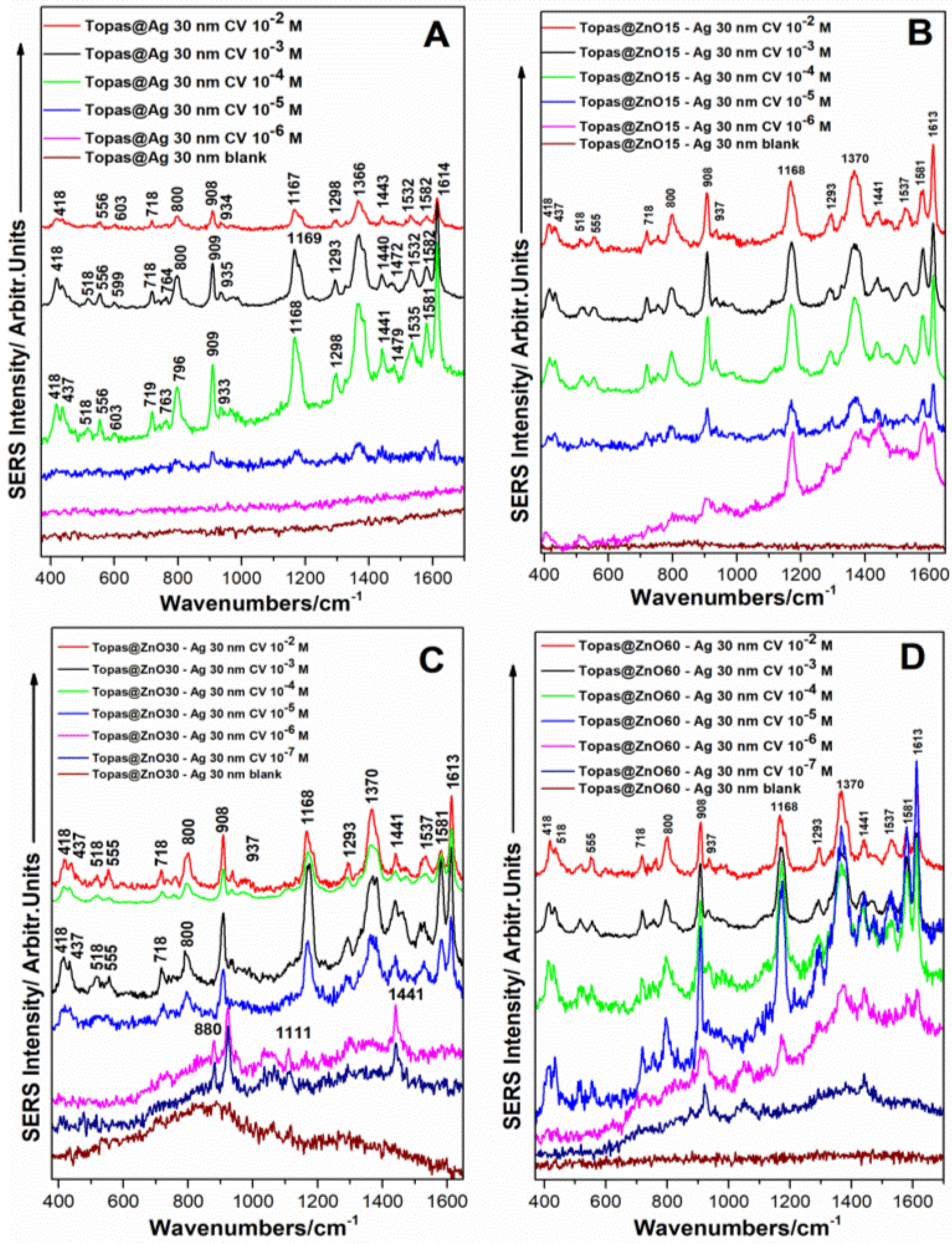
3.3.2. SERS Performance of Ag Films on Topas@ZnO by Using CV as Analyte (30 nm)

In this case, the thickness of the Ag layer was increased and deposited on top of similar, granular ZnO nanostructures obtained on Topas® by using the aforementioned increasing timeline (15, 30, and 60 min, respectively). The SERS analysis of the spectra shown in Figure 6 revealed the ideal conditions for detecting CV with a limit of as low as 10−6 M, with the consistency of the specific spectral fingerprint. The ratio between the thick Ag film on top and the nanostructures with increasing granular islands beneath is not the optimum choice for trace level detection.

3.3.3. SERS Performance of Ag Films on Topas2@ZnO by Using CV as Analyte (7 nm)

The SERS spectra obtained on Topas2-based surfaces are shown in the adjacent Figure 7. Although the SERS spectra obtained at a CV solution concentration of 10−9 M are also shown, the signal from the analyte is completely covered by the significant signal specific to the substrate, as demonstrated in Figure S6. Figure S7 represents the Raman spectra of CV aqueous solutions on a plain plastic substrate.
Conclusively, SERS analysis performed on the ZnO@Ag hybrid films by using CV was achieved with a LOD of 10−7 M in the case of 15 nm thick Ag/Zeonor interlayer films ZnO. A thin Ag film (7–15 nm) on top of the ZnO granular nanostructures was shown to facilitate the enhancement of the Raman signal and to increase the overall SERS performance of the fabricated substrate. The 15 nm Ag/Zeonor® and 30 nm/Topas® films deposited over the ZnO interlayers were continuous with uniform and similar aspects, but the thickness of the Ag film was found to be definitory for the enhancement mechanism. More precisely, the 30 nm thick in-house hybrid films were found to have lower EFs of the Raman signal and lower efficiency in the SERS effect.

4. Discussion

Nanostructured ZnO thin films have been typically grown using physical deposition techniques, such as PLD, molecular beam epitaxy, RF and DC MS, reactive evaporation, or spray pyrolysis. Among these, MS is one of the most accessible and scalable (up to 3 × 6 m2) [65,66] methods for RT growth of textured and c-axis oriented hexagonal zincite crystallites perpendicular to the substrate surface [65]. Polycrystalline ZnO films with a (002) orientation have been grown on glass substrates in O2 partial pressure by means of DC MS [67]. This technique improved adhesion, and greater uniformity of ZnO films was demonstrated at low deposition temperatures and over large area surfaces [67,68].
The tunability of the physical properties and the mechanical stress of the thin films are highly dependent on the growth parameters, such as deposition rate, O2 partial pressure, sputtering pressure, substrate-target distance, substrate temperature, or sputtering power. Ismail et al. [69] revealed that an increase of the RF power above 175 W will likely reduce the tensile strain in the ZnO films deposited on silicon (Si) (100) and glass substrates. An increased O2 flow rate improved the optical transparency and transition from oxygen sub- to over-stoichiometry in the case of ZnO films on silica and (0001)-sapphire substrates [70], while when the Ar:O ratio was increased, an enhanced crystallite size and higher surface roughness values were observed in case of ZnO deposited on corning glass substrate using MS [71]. An increase in the grain size was also observed by Costa et al. [72] when deposition time and the flow of O2 gas were increased, while the roughness varied very little (about 1 nm). An increase in film thickness (up to 280 nm) also influences the shape of the ZnO grains on glass, from spheres to longitudinal shapes [73]. Moreover, when ZnO films deposited on quartz at RT underwent an annealing treatment, the crystalline quality and the grain size increased as a result of an increased annealing temperature and relaxed the residual compressive strain [74].
When the deposition is performed on amorphous substrates, such as glass, the structure of the ZnO thin films appears as well-defined spherical nanograins, as also shown in an earlier work of Lung et al. [75]. The same grain-like structure was also obtained by Vincze et al. [76] when ZnO thin films were deposited on sapphire using the PLD technique. In comparison to these reports, Kaim et al. [77] analyzed the influence of substrate temperature on thin film growth and concluded that larger crystallite formation and better adhesion take place at a temperature of 300 °C.
The growth of ZnO films on flexible substrates has been intensively reported in the light of new flexible and transparent electronic and photonic devices based on ZnO [52,78,79]. Ribut et al. [52] deposited ZnO thin films on Si, sapphire, polyethylene terephthalate (PET), and polypropylene carbonate (PPC) by RF MS at RT. By X-ray diffraction measurements, they demonstrated that the wurtzite structure can be successfully attained also on thermoplastic polymers, and the crystallinity of the films deposited on PET and PPC was higher than those grown on Si and sapphire. When ZnO amorphous films were deposited on another thermoplastic polymer (polyethylene naphthalate PEN) using sol–gel spin-coating method, a thermal dissipation annealing treatment changed the crystal phase to crystalline [56], with applications in optoelectronic devices.
In the case of ZnO thin films deposited on Zeonor® or Topas®-related substrates, the literature is scarce. Only Inguva et al. [55] conducted a systematic study for RT PLD deposition of ZnO thin films on Zeonor® to assess the effect of O2 pressure and the thickness on the surface morphology, hydrophobicity, growth rate, optical and electrical properties. In our study, by collecting relevant SEM, EDX, and SERS data for various combinations of Ag thin films with controlled thicknesses and ZnO nanostructures deposited during an increasing timeline, we were able to obtain a comprehensive characterization of the in-house fabricated substrates.
The SERS analysis of the CV analyte on all the substrates reported herein revealed its specific behavior during the interaction with the substrate. Particularly, when examining the intensity and position variations and shifts of the CV marker bands in Figure 6 and Figure 7, the most dramatical changes appear in the case of the intensity and a little alteration of the position due to the surface proximity. This has also been observed by Canamares et al. [80], who concluded that only a weak physisorption takes place between the CV analyte and the surface. The biggest shift in the band position was observed in the case of the band assigned to νs(CCcenterC)/ν(CN) [80] or CH out of plane bending [50], which appears to shift from 751 to 762 cm−1.
Table 1 summarizes the LODs obtained for each substrate and the calculated analytical EF by considering the intensities of the main marker bands of the CV molecule [9]. We decided as an LOD the presence of at least three marker bands in a SERS spectrum with moderate intensity. Thus, for the detection of CV, we reached the following limits: 10−7 M for Zeonor® and Topas® substrates and 10−9 M for Topas2 substrate. As an observation, the thinner Ag film (7 nm) on top of the ZnO interlayer shows the best SERS enhancement, as shown in Figure 7C,D. ZnO, in this case, shows a significant role that might be more dominant when the silver on top is present in a film with a thickness less than that of the ZnO interlayer thickness. Probably the growth mode is contributing to these conditions in a more significant manner to the overall enhancement mechanism. However, we are reserved in considering as part of the fingerprint of CV molecule the bands found at 908–911, 1436–1441, or 452 cm−1, respectively, even if they are observed with significant contribution to the overall signal because they are also present on the Topas 2 thermoplastic SERS signature (Figure S8).

5. Conclusions

We report on fabricating an affordable physical film with a 3D tunable SERS active surface by employing commercial thermoplastic substrates, a ZnO-based interlayer, and Ag thin film deposition.
Our newly developed substrates possess several key aspects given by the three types of flexible layers as support material: Its applicability as on-demand use—it can be cut to any shape and size, the good adherence of ZnO on plastic limits its degradation when washed, swabbed or wrapped on other types of samples, light-weight with a thickness down to 140 μm, which assures both mechanical resistivity, flexibility and stability of the SERS signal, as well as detection accuracy and high compatibility with portable Raman devices for on-field detection.
The deposition of ZnO and Ag thin films was made following easy, accessible, and scalable protocols with great potential for universal use and low costs. The developed SERS substrates yield reproducible results as compared to colloidal suspensions. Moreover, the use of ZnO overcomes the optical instability of Ag and limits its aggregation.
To assess the quality of the micro/nanostructures resulting from ZnO and Ag growth, scanning electron microscopy (SEM) was employed. High-resolution images of the scanned samples offered definitive information regarding the surface topography/composition of the samples. Valuable conclusions regarding the deposition of ZnO thin films on thermoplastic substrates: (i) The appearance of the ZnO films is due to the existence of nucleation centers to which the material clusters adhere, forming the conglomerates observed by SEM microscopy, (ii) post-deposition mechanical handling of ZnO films on Topas® induced defects (macroscopic cracks), making this substrate unsuitable for future experiments, (iii) ZnO films deposited on Zeonor® and Topas® have identical morphological properties as can be seen from the SEM characterization, while the films deposited on Topas® type 2, after a short deposition time, presented a heterogeneous appearance, with large spaces between the ZnO platelets formats.
Regarding the impact of the “sandwich” structure of the substrate on SERS performance, it is desirable that Ag films with small thicknesses (below 20 nm) are employed. The base substrate has a minimal impact on the way the film is formed (shown on thermoplastic and glass, comparatively). SERS analysis performed on these ZnO-Ag hybrid films using the CV molecule as a detection analyte reached a LOD of 10−7 M in the case of 15 nm thick Ag/Zeonor® films with ZnO interlayer, with relative standard deviation values between 2 and 10%.

Supplementary Materials

The following supporting information can be downloaded at: https://www.mdpi.com/article/10.3390/chemosensors11080441/s1, Table S1: The detailed parameters of MS deposition at RT for ZnO thin films; Figure S1: Representative SEM images (left) and EDX spectra (right) of ZnO films deposited on glass by PLD at RT in O2 bleeding gas and several laser pulses of 7200 and 14,400, respectively. The growth mode of the films is similar to that of the MS-deposited films on Zeonor® and Topas® with a granular structure without defects or voids. This may also be because both glass and polymer films have an amorphous structure. EDX spectra show the amount of O and Zn present in the deposited films. Along with the increase in the number of laser pulses, there was a slight increase in the Zn content; Table S2: The detailed parameters of MS deposition at RT for Ag thin films on top of ZnO nanostructures; Figure S2: Comparative EDX spectra confirming the film growth and proportional increasing of Zn and O elements in concordance with the increasing deposition time in the ZnO films deposited on (a) Zeonor, (b) Topas® and (c) Topas@2; Figure S3: Comparative EDX spectra confirming the Ag film growth and proportional increasing of Ag element in the hybrid samples on (a) Zeonor, (b) Topas® and (c) Topas@2; Figure S4. Comparative SERS spectra showing the reproducibility of the fingerprint of CV aqueous solutions on Zeonor® (A–D), Topas® (EH) and Topas type 2 (IL). All SERS spectra were measured using a laser power of 5 mW, 10 s/accumulation and 2 accumulations/spectrum. Figure S5. SEM micrographs showing defects in Topas@30 (left) and Topas@60 (right) samples; Figure S6: Representative SERS signal from the Topas type 2 substrate obtained after Ag thin film deposition. Figure S7. Representative Raman signal of CV aqueous solution of different concentrations on Zeonor® in comparison with the empty plastic substrate Raman signal.

Author Contributions

Conceptualization, A.C., D.M. and N.E.D.; methodology, A.C., D.M. and I.A.B.; validation, I.A.B., M.S. and N.E.D.; formal analysis, D.M., I.A.B., M.S. and N.E.D.; investigation, A.C., I.A.B. and M.S.; visualization, I.A.B. and M.S.; data curation, A.C. and N.E.D.; writing—original draft preparation, A.C., N.E.D. and D.M.; writing—review and editing, A.C. and N.E.D.; project administration, A.C. All authors have read and agreed to the published version of the manuscript.

Funding

A.C., D.M. and M.S. acknowledge financial support from the Ministry of Research, Innovation and Digitization (MRID), CNCS—UEFISCDI, project number PN-III-P1-1.1-TE-2021-0753, within PNCDI III. I.A.B. acknowledges financial support from the MCID through the “Nucleu” Programe within the National Plan for Research, Development and Innovation 2022–2027, project PN 23 24 01 02. N.E.D. acknowledges the National Research and Development System, Subprogram 1.2—Institutional Performance—Funding Projects for Excellence in RDI, Contract No. 37PFE/30.12.2021.

Institutional Review Board Statement

Not applicable.

Informed Consent Statement

Not applicable.

Data Availability Statement

Not applicable.

Conflicts of Interest

The authors declare no conflict of interest. The funders had no role in the design of the study; in the collection, analyses, or interpretation of data; in the writing of the manuscript; or in the decision to publish the results.

References

  1. Butt, M.A. Thin-film coating methods: A successful marriage of high-quality and cost-effectiveness: A brief exploration. Coatings 2022, 12, 1115. [Google Scholar] [CrossRef]
  2. Chen, Q.; Zhao, L.; Liu, H.; Ding, Q.; Jia, C.; Liao, S.; Cheng, N.; Yue, M.; Yang, S. Nanoporous silver nanorods as surface-enhanced Raman scattering substrates. Biosens. Bioelectron. 2022, 202, 114004. [Google Scholar] [CrossRef]
  3. Fu, B.-B.; Tian, X.-D.; Song, J.-J.; Wen, B.-Y.; Zhang, Y.-J.; Fang, P.-P.; Li, J.-F. Self-calibration 3D hybrid SERS substrate and its application in quantitative analysis. Anal. Chem. 2022, 94, 9578–9585. [Google Scholar] [CrossRef]
  4. Caridad, J.M.; Winters, S.; McCloskey, D.; Duesberg, G.S.; Donegan, J.F.; Krstić, V. Hot-volumes as uniform and reproducible SERS-detection enhancers in weakly-coupled metallic nanohelices. Sci. Rep. 2017, 7, srep45548. [Google Scholar] [CrossRef] [Green Version]
  5. Chen, H.-Y.; Lin, M.-H.; Wang, C.-Y.; Chang, Y.-M.; Gwo, S. Large-scale hot spot engineering for quantitative SERS at the single-molecule scale. J. Am. Chem. Soc. 2015, 137, 13698–13705. [Google Scholar] [CrossRef]
  6. Teutoburg-Weiss, S.; Soldera, M.; Bouchard, F.; Kreß, J.; Vaynzof, Y.; Lasagni, A.F. Structural colors with embedded anti-counterfeit features fabricated by laser-based methods. Opt. Laser Technol. 2022, 151, 108012. [Google Scholar] [CrossRef]
  7. Sripradit, A.; Theeradejvanichkul, T. A self-color-changing film with periodic nanostructure for anti-counterfeit application. Appl. Sci. 2022, 12, 6776. [Google Scholar] [CrossRef]
  8. Lim, K.T.P.; Liu, H.; Liu, Y.; Yang, J.K.W. Holographic colour prints for enhanced optical security by combined phase and amplitude control. Nat. Commun. 2019, 10, 25. [Google Scholar] [CrossRef] [PubMed] [Green Version]
  9. Colniță, A.; Marconi, D.; Dina, N.E.; Brezeștean, I.; Bogdan, D.; Turcu, I. 3D silver metallized nanotrenches fabricated by nanoimprint lithography as flexible SERS detection platform. Spectrochim. Acta Part A Mol. Biomol. Spectrosc. 2022, 276, 121232. [Google Scholar] [CrossRef]
  10. Li, N.; Xu, G.; Yan, M.; Chen, B.; Yuan, Y.; Zhu, C. Fabrication of vertically aligned ZnO nanorods modified with dense silver nanoparticles as effective SERS substrates. Chemosensors 2023, 11, 210. [Google Scholar] [CrossRef]
  11. Li, Z.; Huang, X.; Lu, G. Recent developments of flexible and transparent SERS substrates. J. Mater. Chem. C 2020, 8, 3956–3969. [Google Scholar] [CrossRef]
  12. Zeman, E.J.; Schatz, G.C. An accurate electromagnetic theory study of surface enhancement factors for silver, gold, copper, lithium, sodium, aluminum, gallium, indium, zinc, and cadmium. J. Phys. Chem. 1987, 91, 634–643. [Google Scholar] [CrossRef]
  13. Colniță, A.; Toma, V.-A.; Brezeștean, I.A.; Tahir, M.A.; Dina, N.E. A review on integrated ZnO-based SERS biosensors and their potential in detecting biomarkers of neurodegenerative diseases. Biosensors 2023, 13, 499. [Google Scholar] [CrossRef]
  14. Pérez-Jiménez, A.I.; Lyu, D.; Lu, Z.; Liu, G.; Ren, B. Surface-enhanced Raman spectroscopy: Benefits, trade-offs and future developments. Chem. Sci. 2020, 11, 4563–4577. [Google Scholar] [CrossRef] [Green Version]
  15. Centeno, A.; Aid, S.R.; Xie, F. Infra-red plasmonic sensors. Chemosensors 2018, 6, 4. [Google Scholar] [CrossRef] [Green Version]
  16. Bellingeri, A.; Scattoni, M.; Venditti, I.; Battocchio, C.; Protano, G.; Corsi, I. Ecologically based methods for promoting safer nanosilver for environmental applications. J. Hazard. Mater. 2022, 438, 129523. [Google Scholar] [CrossRef] [PubMed]
  17. Ihtisham, M.; Noori, A.; Yadav, S.; Sarraf, M.; Kumari, P.; Brestic, M.; Imran, M.; Jiang, F.; Yan, X.; Rastogi, A. Silver nanoparticle’s toxicological effects and phytoremediation. Nanomaterials 2021, 11, 2164. [Google Scholar] [CrossRef]
  18. Pham, T.T.H.; Vu, X.H.; Dien, N.D.; Trang, T.T.; Chi, T.T.K.; Phuong, P.H.; Nghia, N.T. Ag nanoparticles on ZnO nanoplates as a hybrid SERS-active substrate for trace detection of methylene blue. RSC Adv. 2022, 12, 7850–7863. [Google Scholar] [CrossRef]
  19. Chen, X.; Zhu, L.; Ma, Z.; Wang, M.; Zhao, R.; Zou, Y.; Fan, Y. Ag nanoparticles decorated ZnO nanorods as multifunctional SERS substrates for ultrasensitive detection and catalytic degradation of Rhodamine B. Nanomaterials 2022, 12, 2394. [Google Scholar] [CrossRef]
  20. Pangpaiboon, N.; Amsiri, T.; Kalasung, S.; Chananonnawathorn, C.; Patthanasettakul, V.; Horprathum, M.; Nuntawong, N.; Limwichean, S.; Eiamchai, P. Controllable decoration of Au NPs on zinc oxide nanorods template by magnetron sputtering technique for reusable-SERS active surface enhancement. AIP Conf. Proc. 2018, 2010, 020023. [Google Scholar] [CrossRef]
  21. He, H.; Li, H.; Xia, W.; Shen, X.; Zhou, M.; Han, J.; Zeng, X.; Cai, W. Electrophoretic fabrication of silver nanostructure/zinc oxide nanorod heterogeneous arrays with excellent SERS performance. J. Mater. Chem. C 2015, 3, 1724–1731. [Google Scholar] [CrossRef]
  22. Xu, J.-Q.; Duo, H.-H.; Zhang, Y.-G.; Zhang, X.-W.; Fang, W.; Liu, Y.-L.; Shen, A.-G.; Hu, J.-M.; Huang, W.-H. Photochemical synthesis of shape-controlled nanostructured gold on zinc oxide nanorods as photocatalytically renewable sensors. Anal. Chem. 2016, 88, 3789–3795. [Google Scholar] [CrossRef] [PubMed]
  23. Pal, A.K.; Pagal, S.; Prashanth, K.; Chandra, G.K.; Umapathy, S.; Mohan, D.B. Ag/ZnO/Au 3D hybrid structured reusable SERS substrate as highly sensitive platform for DNA detection. Sens. Actuators B Chem. 2019, 279, 157–169. [Google Scholar] [CrossRef]
  24. Sakir, M.; Salem, S.; Sanduvac, S.T.; Sahmetlioglu, E.; Sarp, G.; Onses, M.S.; Yilmaz, E. Photocatalytic green fabrication of Au nanoparticles on ZnO nanorods modified membrane as flexible and photocatalytic active reusable SERS substrates. Colloids Surf. A Physicochem. Eng. Asp. 2019, 585, 124088. [Google Scholar] [CrossRef]
  25. Chou, C.M.; Thanh Thi, L.T.; Quynh Nhu, N.T.; Liao, S.Y.; Fu, Y.Z.; Hung, L.V.T.; Hsiao, V.K. Zinc oxide nanorod surface-enhanced Raman scattering substrates without and with gold nanoparticles fabricated through pulsed-laser-induced photolysis. Appl. Sci. 2020, 10, 5015. [Google Scholar] [CrossRef]
  26. Dong, S.; Fu, X.; Zhu, Z.; Li, C. Silver nanorods array on the zinc oxide thin film deposited by hydrothermal methods for surface-enhanced Raman scattering. Appl. Sci. 2022, 12, 9275. [Google Scholar] [CrossRef]
  27. Doanh, T.T.; Van Hieu, N.; Trang, T.N.Q.; Thu, V.T.H. In situ synthesis of hybrid zinc oxide-silver nanoparticle arrays as a powerful active platform for surface-enhanced Raman scattering detection. J. Sci. Adv. Mater. Devices 2021, 6, 379–389. [Google Scholar] [CrossRef]
  28. Wang, C.; Xu, X.; Qiu, G.; Ye, W.; Li, Y.; Harris, R.A.; Jiang, C. Group-targeting SERS screening of total benzodiazepines based on large-size (111) faceted silver nanosheets decorated with zinc oxide nanoparticles. Anal. Chem. 2021, 93, 3403–3410. [Google Scholar] [CrossRef]
  29. Cao, J.; Zhai, Y.; Tang, W.; Guo, X.; Wen, Y.; Yang, H. ZnO tips dotted with Au nanoparticles—Advanced SERS determination of trace nicotine. Biosensors 2021, 11, 465. [Google Scholar] [CrossRef]
  30. Sun, Q.; Xu, Y.; Gao, Z.; Zhou, H.; Zhang, Q.; Xu, R.; Zhang, C.; Yao, H.; Liu, M. High-performance surface-enhanced Raman scattering substrates based on the ZnO/Ag core-satellite nanostructures. Nanomaterials 2022, 12, 1286. [Google Scholar] [CrossRef]
  31. Cook, A.L.; Carson, C.S.; Marvinney, C.E.; Giorgio, T.D.; Mu, R.R. Sensing trace levels of molecular species in solution via zinc oxide nanoprobe Raman spectroscopy. J. Raman Spectrosc. 2017, 48, 1116–1121. [Google Scholar] [CrossRef]
  32. Ashok Kumar, E.; Riswana Barveen, N.; Wang, T.-J.; Kokulnathan, T.; Chang, Y.-H. Development of SERS platform based on ZnO multipods decorated with Ag nanospheres for detection of 4-nitrophenol and rhodamine 6G in real samples. Microchem. J. 2021, 170, 106660. [Google Scholar] [CrossRef]
  33. Huang, C.; Jiang, S.; Kou, F.; Guo, M.; Li, S.; Yu, G.; Zheng, B.; Xie, F.; Zhang, C.; Yu, H.; et al. Development of jellyfish-like ZnO@Ag substrate for sensitive SERS detection of melamine in milk. Appl. Surf. Sci. 2022, 600, 154153. [Google Scholar] [CrossRef]
  34. Barbillon, G. Fabrication and SERS performances of metal/Si and metal/ZnO nanosensors: A review. Coatings 2019, 9, 86. [Google Scholar] [CrossRef] [Green Version]
  35. Wang, X.; Zhang, E.; Shi, H.; Tao, Y.; Ren, X. Semiconductor-based surface enhanced Raman scattering (SERS): From active materials to performance improvement. Analyst 2022, 147, 1257–1272. [Google Scholar] [CrossRef]
  36. Barbillon, G. Latest novelties on plasmonic and non-plasmonic nanomaterials for SERS sensing. Nanomaterials 2020, 10, 1200. [Google Scholar] [CrossRef]
  37. Murthy, S.; Effiong, P.; Fei, C.C. Chapter 11—Metal oxide nanoparticles in biomedical applications. In Metal Oxide Powder Technologies; Al-Douri, Y., Ed.; Elsevier: Amsterdam, The Netherlands, 2020; pp. 233–251. [Google Scholar]
  38. Gao, J.; Wu, B.; Cao, C.; Zhan, Z.; Ma, W.; Wang, X. Unraveling the dynamic evolution of Pd Species on Pd-Loaded ZnO nanorods for different hydrogen sensing behaviors. ACS Sustain. Chem. Eng. 2021, 9, 6370–6379. [Google Scholar] [CrossRef]
  39. Sha, R.; Basak, A.; Maity, P.C.; Badhulika, S. ZnO nano-structured based devices for chemical and optical sensing applications. Sens. Actuators Rep. 2022, 4, 100098. [Google Scholar] [CrossRef]
  40. Ortiz-Casas, B.; Galdámez-Martínez, A.; Gutiérrez-Flores, J.; Ibañez, A.B.; Panda, P.K.; Santana, G.; de la Vega, H.A.; Suar, M.; Rodelo, C.G.; Kaushik, A.; et al. Bio-acceptable 0D and 1D ZnO nanostructures for cancer diagnostics and treatment. Mater. Today 2021, 50, 533–569. [Google Scholar] [CrossRef]
  41. Zhang, M.-L.; Fan, X.; Zhou, H.-W.; Shao, M.-W.; Zapien, J.A.; Wong, N.-B.; Lee, S.-T. A High-efficiency surface-enhanced Raman scattering substrate based on silicon nanowires array decorated with silver nanoparticles. J. Phys. Chem. C 2010, 114, 1969–1975. [Google Scholar] [CrossRef]
  42. Otto, A. Theory of first layer and single molecule surface enhanced Raman scattering (SERS). Phys. Status Solidi A 2001, 188, 1455–1470. [Google Scholar] [CrossRef]
  43. Bell, S.E.J.; Charron, G.; Cortés, E.; Kneipp, J.; De La Chapelle, M.L.; Langer, J.; Procházka, M.; Tran, V.; Schlücker, S. Towards reliable and quantitative surface-enhanced Raman scattering (SERS): From key parameters to good analytical practice. Angew. Chem. Int. Ed. Engl. 2020, 59, 5454–5462. [Google Scholar] [CrossRef] [PubMed] [Green Version]
  44. Barbillon, G.; Graniel, O.; Bechelany, M. Assembled Au/ZnO nano-urchins for SERS sensing of the pesticide thiram. Nanomaterials 2021, 11, 2174. [Google Scholar] [CrossRef]
  45. Barbillon, G. Au Nanoparticles Coated ZnO Film for Chemical Sensing by PIERS Coupled to SERS. Photonics 2022, 9, 562. [Google Scholar] [CrossRef]
  46. Tangsuwanjinda, S.; Chen, Y.Y.; Lai, C.H.; Jhou, G.T.; Chiang, Y.W.; Cheng, H.M. Microporous oxide-based surface-enhanced Raman scattering film for quadrillionth detection of mercury ion (II). Processes 2021, 9, 794. [Google Scholar] [CrossRef]
  47. Guillot, N.; de la Chapelle, M.L. The electromagnetic effect in surface enhanced Raman scattering: Enhancement optimization using precisely controlled nanostructures. J. Quant. Spectrosc. Radiat. Transf. 2012, 113, 2321–2333. [Google Scholar] [CrossRef]
  48. Horcas, I.; Fernández, R.; Gómez-Rodriguez, J.M.; Colchero, J.; Gomez-Herrero, J.; Baro, A.M. WSXM: A software for scanning probe microscopy and a tool for nanotechnology. Rev. Sci. Instrum. 2007, 78, 13705. [Google Scholar] [CrossRef] [PubMed] [Green Version]
  49. Smitha, S.; Gopchandran, K.; Smijesh, N.; Philip, R. Size-dependent optical properties of Au nanorods. Prog. Nat. Sci. 2013, 23, 36–43. [Google Scholar] [CrossRef] [Green Version]
  50. Jones, R.R.; Batten, T.; Smith, B.; Silhanek, A.V.; Wolveron, D.; Valev, V.K. Surface enhanced Raman scattering of crystal violet. In Nonlinear Optics and Applications XII 2021; Bertolotti, M., Zayats, A.V., Zheltikov, A.M., Eds.; SPIE: Virtual, Czech Republic, 2021; Volume 11770. [Google Scholar]
  51. Grys, D.; Chikkaraddy, R.; Kamp, M.; Scherman, O.A.; Baumberg, J.J.; Nijs, B. Eliminating irreproducibility in SERS substrates. J. Raman Spectrosc. 2020, 52, 412–419. [Google Scholar] [CrossRef]
  52. Ribut, S.H.; Abdullah, C.A.C.; Yusoff, M.Z.M. Investigations of structural and optical properties of zinc oxide thin films growth on various substrates. Results Phys. 2019, 13, 102146. [Google Scholar] [CrossRef]
  53. Mauricio, M.R.; Manso, F.C.; Kunita, M.H.; Velasco, D.S.; Bento, A.C.; Muniz, E.C.; de Carvalho, G.M.; Rubira, A.F. Synthesis and characterization of ZnO/PET composite using supercritical carbon dioxide impregnation technology. Compos. Part A Appl. Sci. Manuf. 2011, 42, 757–761. [Google Scholar] [CrossRef]
  54. Ching, C.G.; Ooi, P.K.; Ng, S.S.; Hassan, Z.; Hassan, H.; Abdullah, M.J. Structural properties of zinc oxide thin films deposited on various substrates. Sains Malays. 2014, 43, 923–927. [Google Scholar]
  55. Inguva, S.; Vijayaraghavan, R.K.; McGlynn, E.; Mosnier, J.-P. Highly transparent and reproducible nanocrystalline ZnO and AZO thin films grown by room temperature pulsed-laser deposition on flexible Zeonor plastic substrates. Mater. Res. Express 2015, 2, 096401. [Google Scholar] [CrossRef] [Green Version]
  56. Kim, D.; Leem, J.-Y. Crystallization of ZnO thin films without polymer substrate deformation via thermal dissipation annealing method for next generation wearable devices. RSC Adv. 2021, 11, 876–882. [Google Scholar] [CrossRef] [PubMed]
  57. Chaâbane, N.; i Cabarrocas, P.R.; Vach, H. Trapping of plasma produced nanocrystalline Si particles on a low temperature substrate. J. Non-Cryst. Solids 2004, 338–340, 51–55. [Google Scholar] [CrossRef]
  58. Lu, F.; Guo, Y.; Wang, Y.; Song, W.; Zhao, B. Micro-nano zinc oxide film fabricated by biomimetic mineralization: Designed architectures for SERS substrates. Spectrochim. Acta Part A Mol. Biomol. Spectrosc. 2018, 197, 83–87. [Google Scholar] [CrossRef]
  59. Chuang, K.-T.; Abdullah, H.; Leu, S.-J.; Cheng, K.-B.; Kuo, D.-H.; Chen, H.-C.; Chien, J.-H.; Hu, W.-T. Metal oxide composite thin films made by magnetron sputtering for bactericidal application. J. Photochem. Photobiol. A Chem. 2017, 337, 151–164. [Google Scholar] [CrossRef]
  60. Banholzer, M.J.; Millstone, J.E.; Qin, L.; Mirkin, C.A. Rationally designed nanostructures for surface-enhanced Raman spectroscopy. Chem. Soc. Rev. 2008, 37, 885–897. [Google Scholar] [CrossRef]
  61. Santoro, G.; Yu, S.; Schwartzkopf, M.; Zhang, P.; Vayalil, S.K.; Risch, J.F.H.; Rübhausen, M.A.; Hernández, M.; Domingo, C.; Roth, S.V. Silver substrates for surface enhanced Raman scattering: Correlation between nanostructure and Raman scattering enhancement. Appl. Phys. Lett. 2014, 104, 243107. [Google Scholar] [CrossRef] [Green Version]
  62. Ramadan, R.; Dadgostar, S.; Manso–Silván, M.; Pérez-Casero, R.; Hernandez-Velez, M.; Jimenez, J.; Sanchez, O. Silver-enriched ZnO:Ag thin films deposited by magnetron co-sputtering: Post annealing effects on structural and physical properties. Mater. Sci. Eng. B 2021, 276, 115558. [Google Scholar] [CrossRef]
  63. Zhang, Z.; Yu, J.; Ma, L.; Sun, Y.; Wang, P.; Wang, T.; Peng, S. Preparation of the plasmonic Ag/AgBr/ZnO film substrate for reusable SERS detection: Implication to the Z-scheme photocatalytic mechanism. Spectrochim. Acta Part A Mol. Biomol. Spectrosc. 2019, 224, 117381. [Google Scholar] [CrossRef] [PubMed]
  64. Le Ru, E.C.; Blackie, E.; Meyer, M.; Etchegoin, P.G. Surface enhanced Raman scattering enhancement factors: A comprehensive study. J. Phys. Chem. C 2007, 111, 13794–13803. [Google Scholar] [CrossRef]
  65. Ellmer, K. Magnetron sputtering of transparent conductive zinc oxide: Relation between the sputtering parameters and the electronic properties. J. Phys. D Appl. Phys. 2000, 33, R17–R32. [Google Scholar] [CrossRef]
  66. Szczyrbowski, J.; Dietrich, A.; Hartig, K. Bendable silver-based low emissivity coating on glass. Sol. Energy Mater. 1989, 19, 43–53. [Google Scholar] [CrossRef]
  67. Subramanyam, T.K.; Srinivasulu Naidu, B.; Uthanna, S. Physical properties of zinc oxide films prepared by DC reactive magnetron sputtering at different sputtering pressures. Cryst. Res. Technol. 2000, 35, 1193–1202. [Google Scholar] [CrossRef]
  68. Lee, J.; Lee, D.; Lim, D.; Yang, K. Structural, electrical and optical properties of ZnO:Al films deposited on flexible organic substrates for solar cell applications. Thin Solid Film. 2007, 515, 6094–6098. [Google Scholar] [CrossRef]
  69. Ismail, A.; Abdullah, M. The structural and optical properties of ZnO thin films prepared at different RF sputtering power. J. King Saud Univ. Sci. 2012, 25, 209–215. [Google Scholar] [CrossRef] [Green Version]
  70. Chamorro, W.; Horwat, D.; Pigeat, P.; Miska, P.; Migot, S.; Soldera, F.; Boulet, P.; Mücklich, F. Near-room temperature single-domain epitaxy of reactively sputtered ZnO films. J. Phys. D Appl. Phys. 2013, 46, 235107. [Google Scholar] [CrossRef]
  71. Dave, P.Y.; Patel, K.H.; Chauhan, K.V.; Chawla, A.K.; Rawal, S.K. Examination of Zinc Oxide films prepared by magnetron sputtering. Procedia Technol. 2016, 23, 328–335. [Google Scholar] [CrossRef] [Green Version]
  72. Costa, D.; Borges, J.; Mota, M.F.; Rodrigues, M.S.; Pereira-Silva, P.; Ferreira, A.; Pereira, C.S.; Sampaio, P.; Vaz, F. Effect of microstructural changes in the biological behavior of magnetron sputtered ZnO thin films. J. Vac. Sci. Technol. A 2018, 37, 011501. [Google Scholar] [CrossRef]
  73. Hammad, A.H.; Abdel-Wahab, M.S.; Vattamkandathil, S.; Ansari, A.R. Structural and optical properties of ZnO thin films prepared by RF sputtering at different thicknesses. Phys. B Condens. Matter 2018, 540, 1–8. [Google Scholar] [CrossRef]
  74. Kumar, G.A.; Reddy, M.V.R.; Reddy, K.N. Effect of annealing on ZnO thin films grown on quartz substrate by RF magnetron sputtering. J. Phys. Conf. Ser. 2012, 365, 012031. [Google Scholar] [CrossRef]
  75. Lung, C.; Marconi, D.; Toma, M.; Pop, A. Characterization of the aluminum concentration upon the properties of aluminum zinc oxide thin films. Anal. Lett. 2015, 49, 1278–1288. [Google Scholar] [CrossRef]
  76. Vincze, A.; Bruncko, J.; Michalka, M.; Figura, D. Growth and characterization of pulsed laser deposited ZnO thin films. Open Phys. 2007, 5, 385–397. [Google Scholar] [CrossRef] [Green Version]
  77. Kaim, P.; Lukaszkowicz, K.; Szindler, M.; Szindler, M.M.; Basiaga, M.; Hajduk, B. The influence of magnetron sputtering process temperature on ZnO thin-film properties. Coatings 2021, 11, 1507. [Google Scholar] [CrossRef]
  78. Zhang, Y.-H.; Mei, Z.-X.; Liang, H.-L.; Du, X.-L. Review of flexible and transparent thin-film transistors based on zinc oxide and related materials. Chin. Phys. B 2017, 26, 047307. [Google Scholar] [CrossRef] [Green Version]
  79. Ozgür, Ü.; Alivov, Y.I.; Liu, C.; Teke, A.; Reshchikov, M.A.; Doğan, S.; Avrutin, V.; Cho, S.-J.; Morkoç, H. A comprehensive review of ZnO materials and devices. J. Appl. Phys. 2005, 98, 041301. [Google Scholar] [CrossRef] [Green Version]
  80. Cañamares, M.V.; Chenal, C.; Birke, R.L.; Lombardi, J.R. DFT, SERS, and single-molecule SERS of crystal violet. J. Phys. Chem. C 2008, 112, 20295–20300. [Google Scholar] [CrossRef]
  81. Meng, W.; Hu, F.; Zhang, L.Y.; Jiang, X.H.; Lu, L.D.; Wang, X. SERS and DFT study of crystal violet. J. Mol. Struct. 2013, 1035, 326–331. [Google Scholar] [CrossRef]
Figure 1. Schematic view of the in-house fabrication steps of the hybrid ZnO@Ag flexible thin films.
Chemosensors 11 00441 g001
Figure 2. Representative SEM micrographs showing the ZnO growth on Zeonor®, Topas®, and Topas2 at deposition times of 15 (A,D,G), 30 (B,E,H), and 60 min (C,F,I).
Chemosensors 11 00441 g002
Figure 3. Generated area histograms of the constituent ZnO grains from the ZnO films on Zeonor® (left), Topas® (middle), and Topas@2 (right) flexible substrates.
Chemosensors 11 00441 g003
Figure 4. Representative SEM micrographs showing the ZnO@Ag SERS surfaces on Zeonor® (BD), Topas® (FH), and Topas2 (JL) with Ag film thicknesses of 15 nm (on Zeonor), 30 nm (on Topas®) and 7 nm (on Topas2), respectively ((A,E,I) images present the substrates without ZnO, only Ag thin films on the plastic substrates).
Chemosensors 11 00441 g004
Figure 5. Representative SERS spectra of CV molecule on Zeonor® substrate without ZnO (A), with ZnO film obtained with different deposition times (15—B, 30—C, and 60 min—D, respectively) and covered with 15 nm Ag film on top.
Chemosensors 11 00441 g005
Figure 6. Representative SERS spectra of CV molecule on Topas® substrate without ZnO (A), with ZnO film obtained with different deposition times (15—B, 30—C, and 60 min—D, respectively) and covered with 30 nm Ag film on top.
Chemosensors 11 00441 g006
Figure 7. Representative SERS spectra of CV molecule on Topas® type 2 substrate without ZnO (A), with ZnO film obtained with different deposition times: 15, 30, and 60 min, respectively (BD) and covered with 7 nm Ag film on top.
Chemosensors 11 00441 g007
Table 1. The table summarizes the identified SERS marker bands of the CV analyte in correlation with the LODs and the calculated EFs obtained for each of the fabricated substrate.
CV Raman Bands (cm−1)SERS
Substrates
Limits of Detection (M)AEFs
AssignmentsAg Thin Film AloneZnO-15 and Ag ZnO-30 and Ag ZnO-60 and Ag
1612/1615 vs.Zeonor®ν(C–C)ring [81]10−610−76.9 × 10³
Topas®10−510−610−510−60.5 × 10³
Topas@210−61.2 × 10⁴
1580 mZeonor®ν(C–C)ring [81]10−610−72 × 104
Topas®10−510−610−510−62.5 × 10³
Topas@210−61.7 × 10⁴
1530–1537 mZeonor®ν(CringN)/δs(CH3) [80]10−510−610−74.3 × 10⁴
Topas®10−410−610−52.6 × 10²
Topas@210−510−610−50.7 × 10⁴
1366/1368 sZeonor®νas(CCcenterC)/δ(CCC)ring/δ(CH) [80]10−510−63.5 × 10³
Topas®10−510−610−510−60.8 × 10³
Topas@210−60.7 × 10⁴
1292–1295 mZeonor®νas(CCcenterC)/δ(CCC)ring/δ(CH) [80]10−510−610−73.4 × 10⁴
Topas®10−610−710−60.9 × 10³
Topas@210−510−710−61.7 × 10⁴
1168–1170 vs.Zeonor®νs(CCcenterC)/δ(CCC)breathing/ρr(CH3) [80]10−510−61.3 × 10⁴
Topas®10−510−610−510−61.5 × 10³
Topas@210−510−60.8 × 10⁴
908 vs.Zeonor®δ(CCcenterC) [80]10−710−710−710−71.9 × 10⁴
Topas®10−510−610−71.4 × 10⁴
Topas@210−610−810−910−81.4 × 10⁶
796–804 mZeonor®δin plane(C–H)\,ring [81]10−510−63.5 × 10²
Topas®10−510−610−52.9 × 10²
Topas@210−510−610−53.4 × 10³
555 wZeonor®γ(CCC)/δ(CNC)/δ(CCcenterC) [80]10−510−61.9 × 10³
Topas®10−510−410−52.5 × 10²
Topas@210−51.5 × 10³
υ-stretching vibration; δ-bending deformation; ρ-rocking vibration; γ-out-of-plane deformation.
Disclaimer/Publisher’s Note: The statements, opinions and data contained in all publications are solely those of the individual author(s) and contributor(s) and not of MDPI and/or the editor(s). MDPI and/or the editor(s) disclaim responsibility for any injury to people or property resulting from any ideas, methods, instructions or products referred to in the content.

