1. Introduction
Two-dimensional materials, also known as two-dimensional crystals or 2D materials, are structures with a thickness of one or several atomic layers [
1,
2,
3,
4,
5]. The discovery of graphene, a monoatomic layer of carbon, in 2004 marked a significant breakthrough in the field of two-dimensional materials [
6]. Graphene is a unique two-dimensional allotrope of carbon with atoms arranged in a flat honeycomb lattice. Prior to the discovery of graphene, it was believed that extended two-dimensional crystals could only be stable at temperatures close to absolute zero [
7]. Unlike bulk materials, two-dimensional crystals have a high surface area to volume ratio, which affects their energy structure and electrical and optical properties.
The success in synthesizing graphene sparked interest in exploring other single-element two-dimensional materials (transgraphenes) of groups 13–16 of the periodic table [
8]. Fabricating transgraphene materials is highly promising for the development of future nanodevices, offering increased efficiency and high speed [
9,
10]. Consequently, there has been a significant surge in both theoretical and experimental research focused on two-dimensional nanomaterials. Through the collaborative endeavors of scientists, numerous single-element two-dimensional materials have been successfully synthesized: borophene, gallenene, thallene, silicene, germanene, stanene, plumbene, phosphorene, arsenene, antimonene, bismuthene, selenene and tellurene [
11,
12]. Extensive research is dedicated to exploring the exceptional properties of 2D materials and their potential in revolutionizing device design with novel operating principles [
13,
14,
15,
16,
17,
18,
19,
20]. Particular attention is paid to graphene’s closest neighbors in group 14—silicene and germanene. An important advantage of these two novel materials is its direct compatibility with existing highly developed silicon technology.
Synthesizing transgraphene materials is an extremely challenging task in the present day. Graphene, a single layer of sp
2-hybridized carbon atoms, can be easily obtained by peeling off monolayers from graphite due to weak interlayer interaction [
21,
22,
23]. However, obtaining a monoatomic layer of silicon or germanium is much more difficult due to the sp
3-hybridization of the atoms and the strong covalent bonds. Consequently, exfoliation cannot be used to obtain silicene and germanene. As a result, the primary method for creating graphene-like materials is their epitaxial growth on lattice-matched substrates.
To date, silicene has been successfully synthesized on the surfaces of Ag(111) [
24,
25], Ir(111) [
26], Pb(111) [
27], MoS
2 [
28], ZrC [
29], Ru [
30], while germanene was fabricated on the surfaces of Au(111) [
31], Pt(111) [
32], Al(111) [
33], MoS
2 [
34] and h-AlN [
35]. However, all of the listed substrates are very expensive. In addition, these surfaces require a very complex pre-growth treatment, which most often involves multiple cycles of ion etching and high-temperature annealing, which requires a very large amount of time and additional equipment. There are also problems with producing large-area defect-free sheets and the separation of the resulting layers from the substrate. Therefore, searches are underway for alternative substrates for the production of silicene and germanene.
One of the most promising substrates for growing silicene and germanene is highly oriented pyrolytic graphite (HOPG). Its initial sp
2 configuration perfectly matches the required hexagonal structure of silicene and germanene. Attempts to synthesize silicene and germanene on the surface of HOPG have been made since 2016 [
36,
37], but this result was questioned in [
38] and this question still remains open.
The presented work makes a further attempt to clarify the nature of the epitaxial growth of silicon and germanium layers on the surface of highly oriented pyrolytic graphite in a wide range of temperatures and coverages. A number of studies have already carried out the growth of thin layers, nanocrystals and polycrystalline structures of silicon and germanium on the surface of graphene and HOPG [
39,
40,
41,
42,
43], but, so far, the processes of epitaxial growth have not been studied by the RHEED method. The goal of this work was to establish the time dynamics of changes in diffraction patterns from a growing surface directly during deposition and to reveal temperature intervals for various growth modes of silicon and germanium on HOPG.
2. Materials and Methods
The growth studies presented in this work were carried out using the molecular beam epitaxy (MBE) on a Katun-100 installation. A preliminary vacuum was created by a vacuum station with a turbomolecular pump, and the presence of a degassing system for the epitaxy chamber, magnetic discharge pumps on each chamber, a sublimation pump and cryopanels allowed the pressure in the installation to be maintained at a level of <10−10 Torr during the epitaxial growth of structures. To evaporate Ge and Si materials, electron beam evaporators were used, which have a cooling system that ensures high purity of the material and stability of the evaporation rate of the material. To determine the deposition rate of Ge and Si material, there were two water-cooled quartz resonators with shutters. Shutters were also used to interrupt the flow of materials.
In this work, the epitaxial growth of germanium and silicon on commercially available HOPG wafers was studied. Before epitaxial growth, the top damaged layer of HOPG substrate was removed using acrylic tape. The foamed structure of the acrylic tape ensured the best uniform adhesion to the surface of the sample and uniform tearing of the top layer. Then, HOPG wafer was transferred to a high-vacuum chamber to maintain surface quality. In the growth chamber, it was thermally annealed at 1200 °C. During annealing, the pressure in the chamber was maintained at a level of no more than 3 × 10⁻⁹ Torr. During the annealing process, the release of dissolved gases from the substrate, such as hydrogen, was recorded with the built-in mass spectrometer using the corresponding atomic mass peaks. After annealing, the temperature was dropped to growth temperatures; cooling occurred naturally. The temperature of HOPG substrate in the epitaxial chamber was controlled using an Optics 2.3 µm pyrometer.
The monitoring and analysis of the state of the substrate surface were carried out by reflection high-energy electron diffraction directly during the growth process. A flow of high-energy electrons with energy of 26 keV was directed at a grazing angle of approximately 1° to the HOPG surface and, when reflected from it, formed characteristic diffraction patterns on the luminescent screen. Diffraction patterns were recorded by a video camera connected to a computer. The resulting video signal was recorded and processed in real time, which makes it possible to measure, frame by frame, the change in intensity and the position of the spots of diffraction patterns [
44,
45].
The Raman spectra of the samples were measured using a Raman microscope inVia Reflex system from Renishaw (UK). The Raman microscope is equipped with an RL785-08 laser with an excitation wavelength of 785 nm, a laser beam diameter of 700 ± 100 μm, and an average radiation power of 120 mW. The spectral resolution of the device is 1 cm−1, the lens is Leica L × 50. To obtain spectral data of the samples, the following radiation parameters were selected: exposure time—20 s, radiation power on the sample—10% of the average laser power (12 mW), the number of signal accumulations—1. The spectra were recorded in mapping mode, an area with dimensions of 5 mm × 5 mm was analyzed (4 spatial points with a step of 5 mm), and the two spectral ranges 7–200 cm−1 (low frequency) and 100–3200 cm−1 were used.
Scanning electron microscopy (SEM) investigations were performed using an Apreo S LoVac (Thermo Fisher Scientific, Brno, Czech Republic) scanning electron microscope.
3. Results
3.1. Epitaxial Growth of Si on HOPG
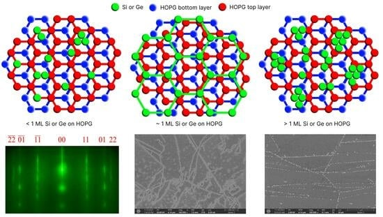
First of all, the original HOPG wafers were studied by reflection high-energy electron diffraction. HOPG sample consists of randomly oriented domains, all of which have the (0001) plane parallel to the surface. As a result, one can observe the diffraction spots from all the possible planes at the same time [
46].
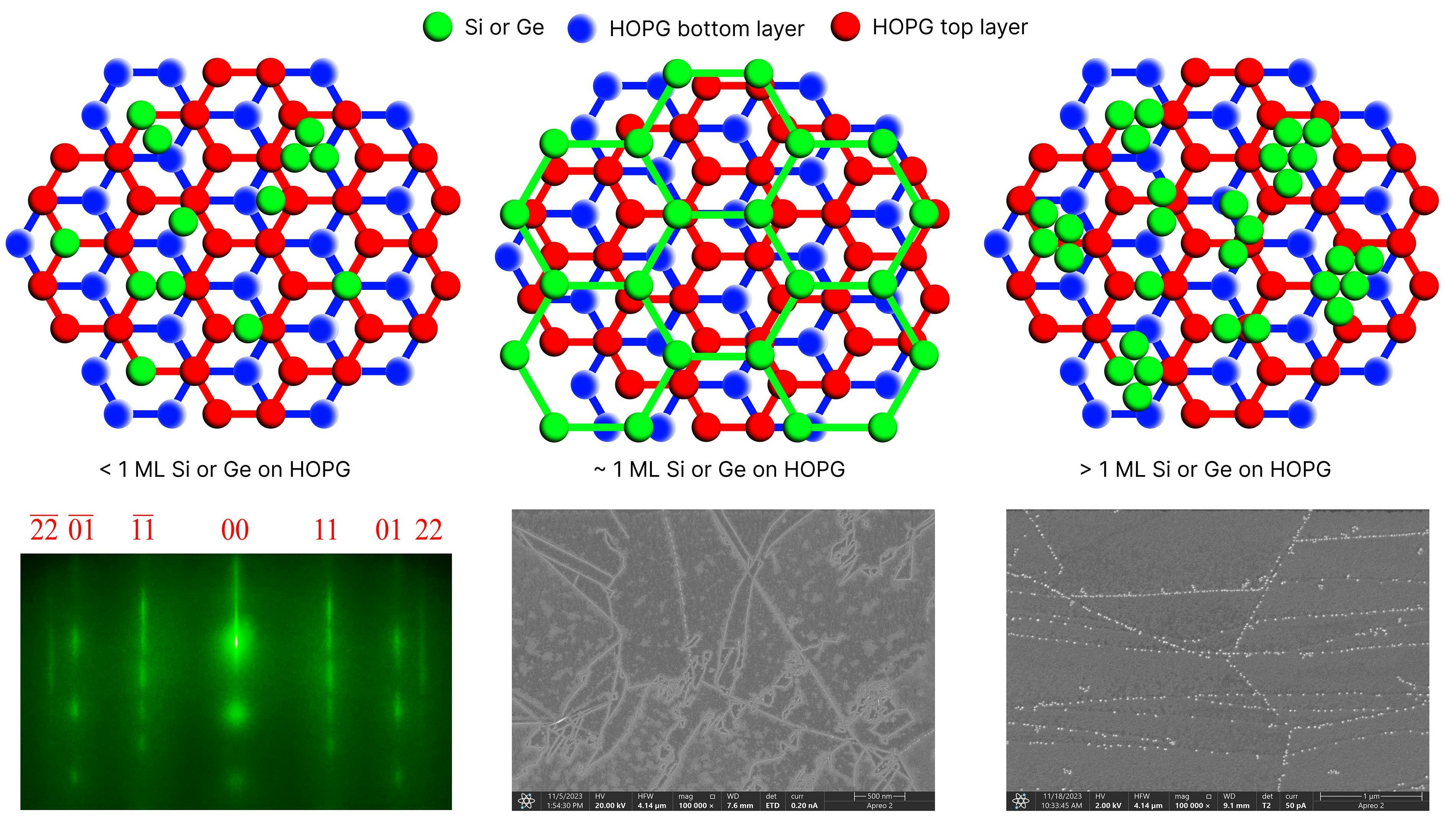
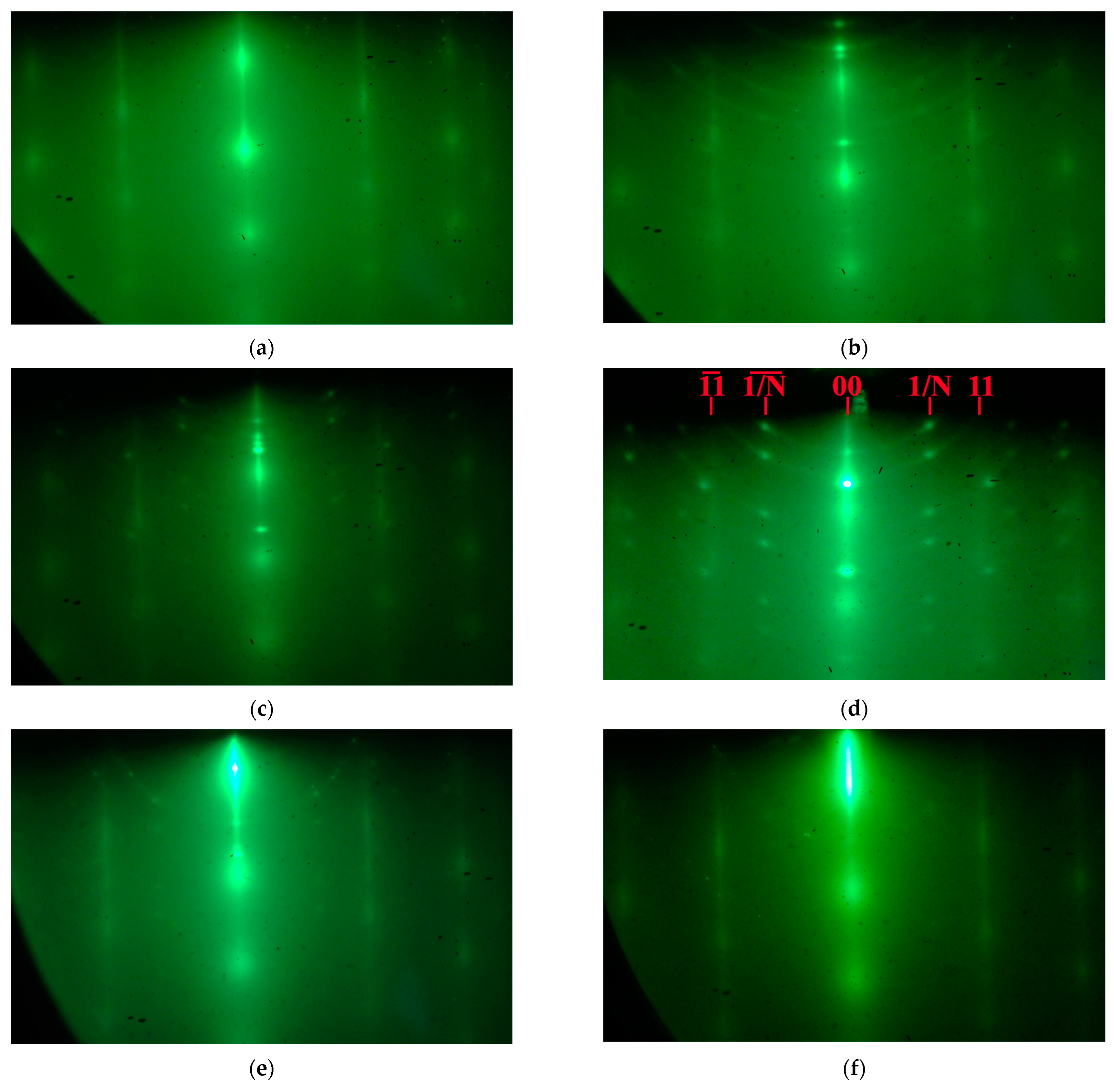
Figure 1 shows the diffraction pattern from a clean HOPG surface.
This diffraction pattern is characterized by the presence of numerous diffraction spots, which form several clearly defined narrow lines (groups of reflections), designated 00, 11, 01, 22, etc. The quality and condition of the surface of the initial HOPG wafers were checked by the presence of clearly identified reflections in the diffraction pattern.
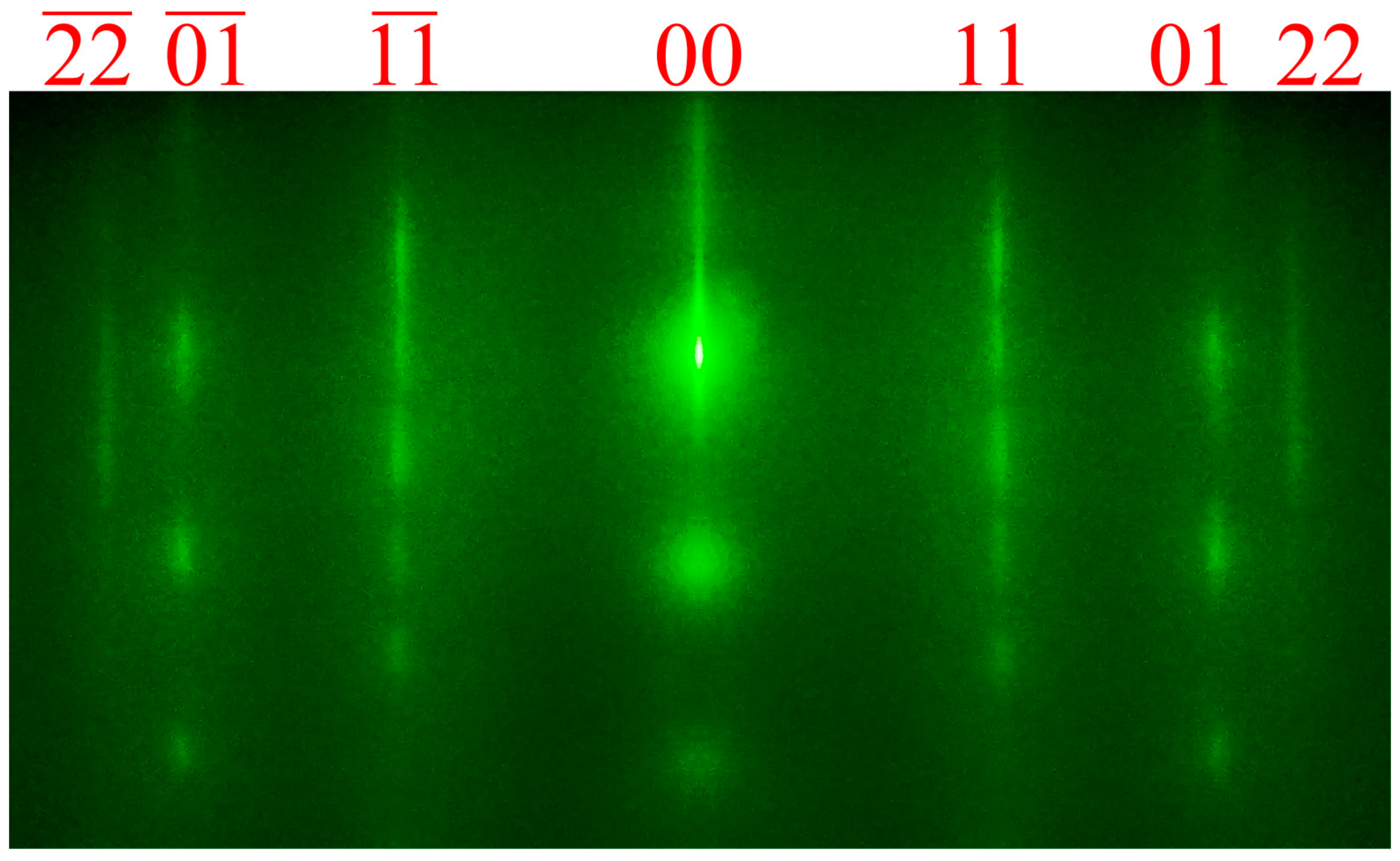
A series of experiments was carried out on the deposition of germanium and silicon on HOPG in a wide range of substrate temperatures. Si growth on HOPG was carried out at temperatures of 100–650 °C at a silicon deposition rate of 0.02 mL/s (monolayers per second).
At 100 °C, silicon grows amorphously on the HOPG surface (
Figure S1a,b). The diffraction pattern after the deposition of 10 mL of Ge at 100 °C represents a homogeneous diffusion background (
Figure 2b). When silicon is deposited onto HOPG at temperatures of 200–600 °C up to a thickness of 1 mL (
Figure S1c–e), the diffraction pattern of the original HOPG does not change (
Figure 2a). In this case, changes are not detected at any of the azimuthal angles when the substrate is rotated. This indicates that, up to this thickness, silicon follows the crystal structure of the substrate. When a larger number of silicon layers is deposited at 200–600 °C, the growth pattern of Si on HOPG approaches polycrystalline growth. The diffraction pattern gradually loses intensity, but not as quickly as at low temperatures. Semicircles (Debye rings) begin to appear on a diffraction screen (
Figure 2c). At a temperature of 650 °C, silicon was deposited first to a thickness of 10 mL (
Figure 2d) and then to 80 mL (
Figure 2e). Up to an effective thickness of deposited silicon of 1 mL, no changes occurred in the diffraction pattern, but, with increasing coverage, a large number of additional reflections and semicircles began to appear, which persisted even at larger silicon thicknesses. An experiment was also carried out to anneal at 590 °C for 60 min a sample with 1 mL of silicon grown at 200 °C (
Figure 2f). No changes in the diffraction pattern occurred during this process. From these results, it may be concluded that additional reflections in the diffraction pattern begin to appear only at temperatures above 650 °C after the deposition of 1 mL of Si.
Attempts have been made to completely anneal silicon from the HOPG surface. However, at annealing temperatures up to 800 °C, it was not possible to restore the original diffraction pattern from a clean HOPG surface, which may indicate the formation of silicon carbide on the substrate surface (
Figure S1f).
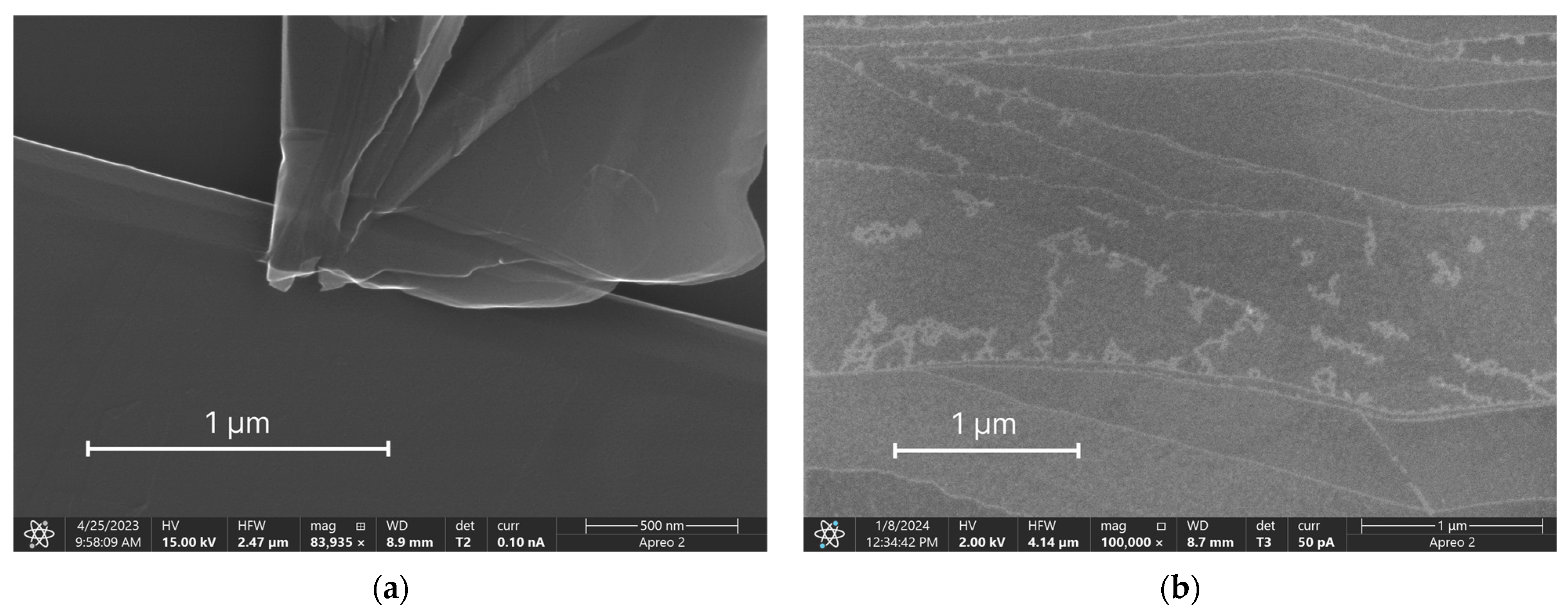
Figure 3 shows the results of investigating the surface of Si/HOPG samples using scanning electron microscopy.
Figure 3a shows an image of the surface of highly oriented pyrolytic graphite before silicon deposition. Smooth terraces are visible and a clear boundary between them (the edge of the step). A graphite flake is also partially visible, the existence of which is possible on some areas of the surface.
Figure 3b shows SEM image of the HOPG surface after the deposition of about 0.9 mL of silicon on HOPG. It can be seen that silicon atoms coalesce as 2D islands on the surface of the HOPG terraces. Moreover, a large part of adatoms diffuse to the edges of the HOPG steps from contiguous regions of the lower adjacent terrace.
3.2. Epitaxial Growth of Ge on HOPG
Ge growth on HOPG was carried out at temperatures of 100–720 °C at a germanium deposition rate of 0.02 mL/s. Before each growth process, the HOPG substrate was annealed at 800 °C for 5 min. It was found that, at a temperature of 800 °C, germanium atoms desorbed from the substrate and the surface were restored to pure HOPG, as evidenced by the characteristic diffraction patterns of clean HOPG surface, as shown in
Figure 4a.
At low temperatures, germanium grew amorphously on HOPG. During the growth of Ge on HOPG at 170 °C, changes began to appear in the diffraction pattern after the deposition of about 2 mL of germanium (
Figure S2a). Then, within 8 mL, the formation of Debye rings with weak point reflections of the 1/
N type occurred (
Figure 4b). The 1/
N reflections were located between the 00 and 11 lines of the original diffraction pattern for HOPG (
Figure 4d) (details are in
Section 4).
When germanium was deposited on HOPG at 250 °C, changes appeared in the diffraction pattern at a thickness of the germanium layer of about 1 mL (
Figure S2b). Then, up to a thickness of about 10 mL, Debye rings were weakly expressed, and 1/
N points were formed (
Figure 4c). For the Ge growth on HOPG at 350–450 °C (
Figure S2c), the Debye rings in the diffraction pattern were moderately expressed and the 1/
N points were most clearly visible starting from 1 mL of germanium (
Figure 4d). For the deposition at 460°C, the number of Ge monolayers required for the appearance of 1/
N reflections significantly increased (
Figure 4e). For the temperatures of 500, 600, and 720 °C, there were no noticeable changes in the diffraction pattern up to thicknesses of about 20 mL (
Figure S2d–f). Further growth was not conducted. This circumstance indicates the predominance of desorption of Ge atoms from the HOPG surface at high deposition temperatures. An experiment was also conducted on 1 mL Ge deposition at 300 °C (
Figure S2g), followed by annealing at 400 °C for 60 min. There were no qualitative changes in the diffraction pattern (
Figure 4f).
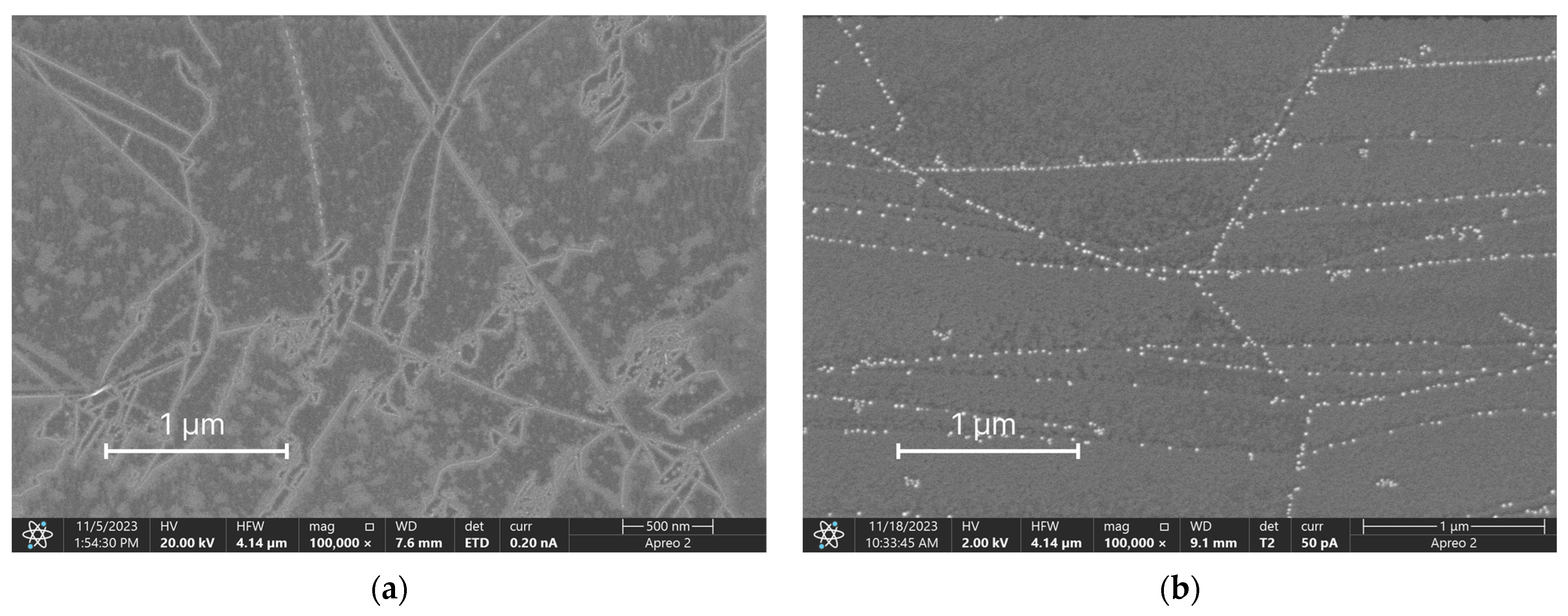
Figure 5 shows the results of investigating the surface of Ge/HOPG samples using scanning electron microscopy.
Figure 5a shows the SEM image of the HOPG surface after the deposition of about 0.9 mL of germanium. From this image, it can be seen that germanium preferentially assembles as elongated nanowires along the edges of the pristine HOPG steps. It should be noted that some of the edges of the terraces are completely filled with germanium atoms (solid light lines), and some are only partially filled (dashed light lines). In addition, there are a large number of regions containing 2D germanium layers that fill the surface of the HOPG terraces in the form of individual 2D islands away from the edges of the steps. At later stages (several monolayers and more) germanium forms chains of small 3D clusters along the HOPG edges (
Figure 5b). The similar formation of chains of 3D clusters has been previously observed by Shimonaka et al. [
47]. They have also studied, in detail, the features of Ge/HOPG deposition at higher germanium coverages (>10 mL of germanium).
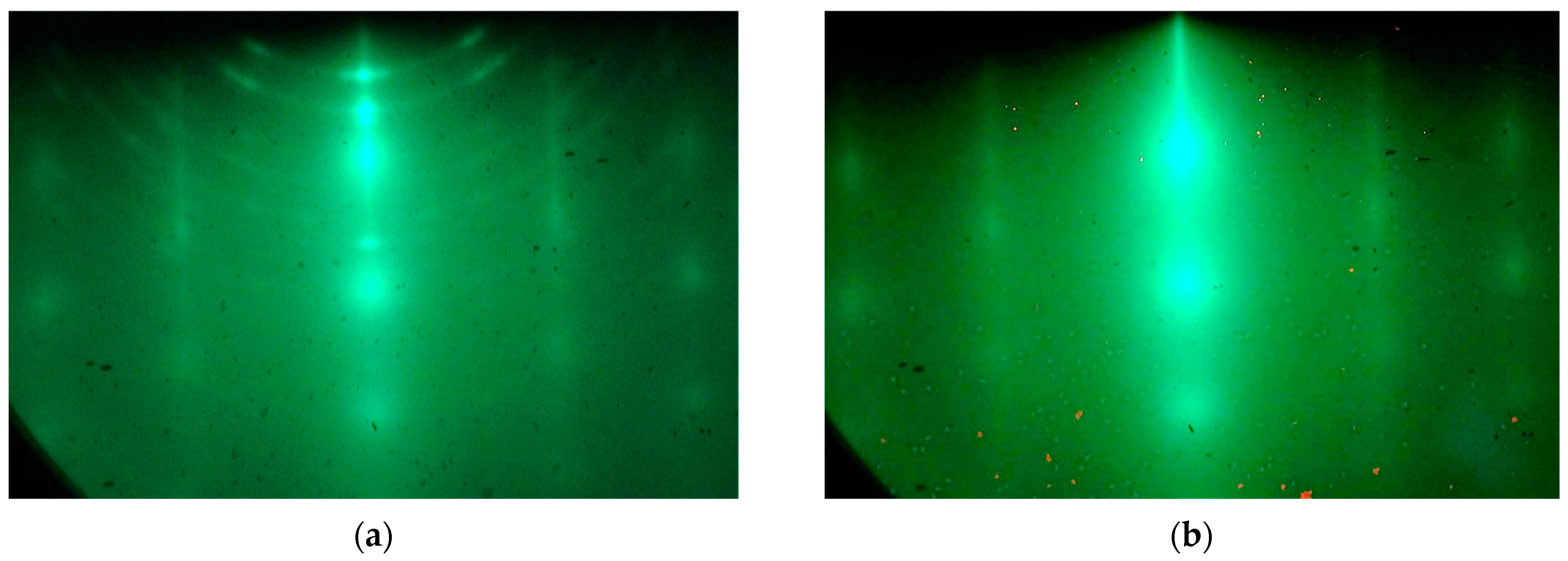
When the Ge/HOPG sample is annealed (
Figure 6a) at temperatures above 800 °C, germanium atoms completely desorb from the surface, as evidenced by the recovery to the characteristic diffraction pattern for clean HOPG surface during the annealing process (
Figure 6b). This is confirmed by the fact that, during the subsequent deposition of Ge at lower temperatures (after annealing), the diffraction pattern changes after 1–2 mL of Ge.
Considering that, up to a deposited material thickness of 1 mL at the same growth rate, there were no changes in the diffraction patterns, a study of the growth of germanium was carried out at a deposition rate of 0.01 mL/s and a temperature of 260 °C (
Figure S2h). It was found that the nature of the change in diffraction patterns for this growth rate is the same.
3.3. Raman Spectroscopy Investigations
Raman spectroscopy studies of the samples with silicon and germanium on the surface of HOPG were carried out.
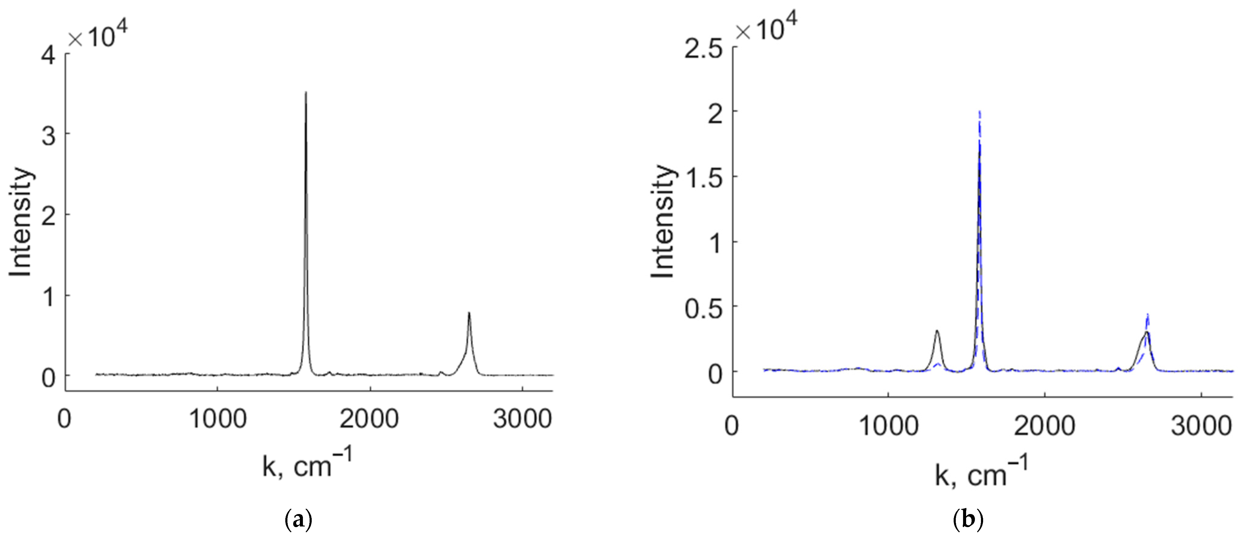
Figure 7a shows the Raman spectrum for the original HOPG sample. The spectrum has a form typical of graphite [
48,
49]. The lines with Raman shift k = 1580 and 2650 cm
−1, characteristic of this substrate, are clearly visible.
Figure 7b shows the Raman spectrum of a sample with about 3 mL silicon layer on HOPG grown at the temperature of 400 °C. The solid line corresponds to the spectrum taken from the side of the deposited silicon layer, and the dotted line corresponds to the spectrum from the back side of the HOPG wafer. A clear peak at k = 1310 cm
−1 is visible. In addition, the peak of the initial graphite surface at 2650 cm
−1 becomes asymmetric and broadened, which also indicates the appearance of an additional peak in the presence of silicon. Typically, these two peaks are associated with the formation of defects on the surface of graphite, which may be due to the deposition of silicon on it. So, for Si/HOPG samples, the Raman spectrum is less convincing on the presence of silicene. Nazzari et al. reported on the presence of a low-frequency Raman band of silicene near 100 cm
−1 [
50]. However, low-frequency (7–200 cm
−1) Raman spectra of the studied samples did not reveal any significant features in our study (
Figures S3 and S4). This may be due to the fact that these bands are expected to have very low intensity for a surface with just 1 mL of deposited material.
Finally,
Figure 8a shows the Raman spectra of the sample with 10 mL germanium on the surface of HOPG, grown at 400 °C.
Figure 8b compares the Raman spectra of a HOPG sample (blue curve) and the 10 mL Ge/HOPG sample (orange curve) near the point k = 300 cm
−1. Due to the small values of the signal, it was necessary to use a special technique for analyzing Raman spectra, developed by the authors [
51]. As a result, the presence of small peaks near 296, 300, and 304 cm
−1, corresponding to germanium, was established. This is consistent with the previous report on germanene, where Jung et al. revealed a Raman band at 296 cm
−1 in a germanene sample [
52]. This line was also predicted theoretically by Kukucska et al. [
53]. The rest of the spectrum corresponded to the spectrum of the HOPG substrate. Low-frequency (7–200 cm
−1) Raman spectra of the studied samples did not reveal any features (
Figure S5).
4. Discussion
From the results obtained, we can conclude that there are clearly defined temperature intervals for the growth of silicon and germanium on HOPG. Within each interval, one or another growth mechanism is realized. Thus, at temperatures close to room temperature, silicon and germanium grow amorphously on the HOPG surface. When the temperature increases above 150 °C, silicon and germanium begin to grow pseudomorphically, and, up to a thickness of 1 mL of the deposited material, their crystal structure repeats the structure of the substrate [
36,
37].
When the amount of deposited material increases above 1 mL, new reflections begin to appear, characterizing different crystalline states of the growing material. Of particular interest are the 1/
N reflections located between reflections 00 and 11 of the original graphite substrate (
Figure 4d). The parameter
N has different values for silicon and germanium. It is defined as the ratio of the distance between 11 and 00 reflections to the distance between 1/
N and 00 reflections.
From the analysis of the obtained diffraction patterns, the value of
N for silicon is
N(Si) = 1.56, and, for germanium, it is equal to
N(Ge) = 1.62. This reflection appears when about 1 mL of silicon or germanium is deposited. Knowing the lattice constant of graphite (0.246 nm), and using the value of the parameter
N, one can determine the periodicity of the structure of the growing material. For silicon,
N(Si) × 0.246 nm = 0.384 nm, and, for germanium,
N(Ge) × 0.246 nm = 0.399 nm [
5,
8]. The obtained values correspond very well to the lattice constants of silicene (0.39 nm) and germanene (0.40 nm), which may indicate the presence of areas of graphene-like 2D phases during epitaxial deposition of silicon and germanium onto the surface of highly oriented pyrolytic graphite. Such regions of the 2D phase can be two-dimensional islands of germanium that fill the surfaces of the HOPG terraces far from the edges of the steps and visualized in SEM images (
Figure 5b).
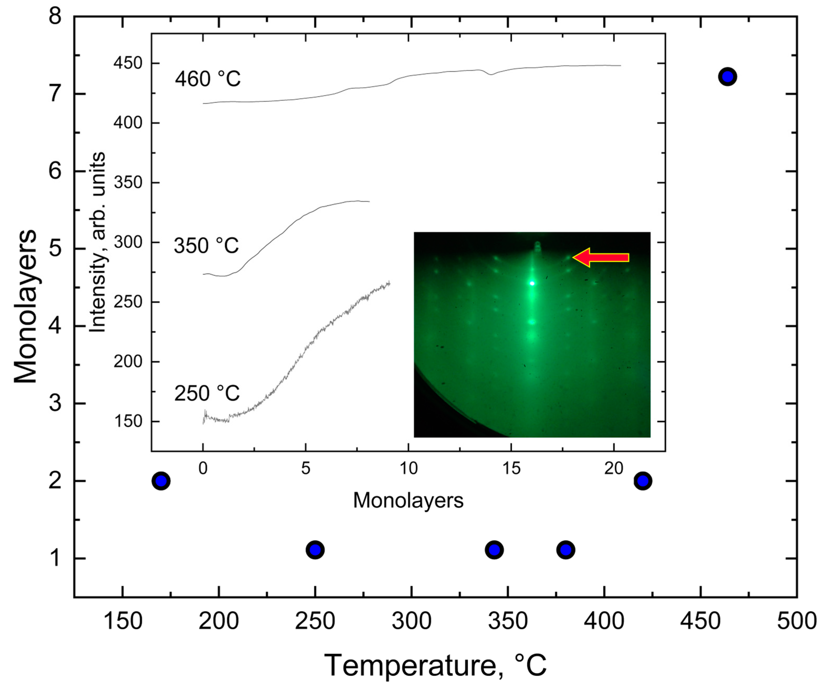
The dynamics of changes in the intensity of
N reflections for different temperatures are nonlinear (
Figure 9).
Figure 9 shows the dependence of the moment of the appearance of an additional 1/
N reflection on the substrate temperature when Ge is deposited on HOPG. The inset to
Figure 9 shows the dependence of the local intensity of the diffraction pattern at the point of formation of the 1/
N reflection on the effective thickness of the deposited germanium on the HOPG surface (which is proportional to the growth time). The Ge growth rate for all curves was the same, equal to 0.02 mL/s. From this graph, it is clear that, at temperatures below 450 °C, the 1/
N reflection appears at an effective thickness of the deposited material of about 1 mL. Then, during the deposition of several monolayers, the intensity of this reflection reaches its maximum stationary value. The absolute intensity value for all curves is approximately the same, and, in the graph, the curves are shifted for clarity. The 1/
N reflections persist for a sufficiently large number of deposited layers.
For temperatures of 450 °C and above, the number of Ge monolayers required for the intensity of the 1/N reflection to reach its maximum value increases significantly. When Ge grows on HOPG at 500 °C and above, there are no noticeable changes in the diffraction pattern. This circumstance indicates the predominance of the rate of the desorption of Ge atoms from the HOPG surface over the rate of adsorption processes.
At later stages (several monolayers and more), silicon and germanium form small 3D clusters along the HOPG edges [
47]. When the Ge/HOPG sample is annealed, germanium atoms completely desorb from the surface. For silicon, it is not possible to anneal the silicon layer on the HOPG surface. This is probably due to the formation of silicon carbide on the surface during the chemical interaction of carbon and silicon atoms.
5. Conclusions
In this work, the epitaxial growth of silicon and germanium was studied directly in the process of material deposition onto the HOPG surface using reflection high-energy electron diffraction. In addition, the obtained samples were studied by scanning electron microscopy and Raman spectroscopy. A wide range of deposition temperatures from 100 to 800 °C was considered. Temperature intervals for various growth regimes of silicon and germanium on highly oriented pyrolytic graphite have been determined. It has been shown that, at temperatures close to room temperature, materials grow amorphously, and, at high temperatures, polycrystalline growth is observed. It has been established that the crystal structure of silicon and germanium within one monolayer repeats the structure of graphite. When the amount of deposited material increases to more than one monolayer in the intermediate temperature range (250–400 °C for germanium and above 650 °C for silicon), reflections of the 1/N type appear in the diffraction pattern (N(Si) = 1.56 and N(Ge) = 1.62). These values correspond to the lattice constants of silicene and germanene and may indicate the presence of areas of graphene-like 2D phases during the epitaxial deposition of silicon and germanium onto the surface of highly oriented pyrolytic graphite. The results obtained can be used to develop technology for the fabrication of silicene and germanene. In addition, the presented results will also be valid for the epitaxial growth of silicon and germanium layers on graphene, since it is single-layer graphite without underlying layers.
Supplementary Materials
The following supporting information can be downloaded at:
https://www.mdpi.com/article/10.3390/c10020036/s1, Figure S1: The characteristic diffraction pattern formed from (a) clean HOPG surface; (b) Si/HOPG surface, growth temperature 100 °C, effective thickness of the deposited silicon 1 mL; (c) Si/HOPG, 200 °C, 1 mL; (d) Si/HOPG, 400 °C, 1 mL; (e) Si/HOPG, 650 °C, 1 mL; (f) HOPG surface after annealing silicon at 800 °C; Figure S2: The characteristic diffraction pattern formed from (a) Ge/HOPG surface, growth temperature 170 °C, effective thickness of deposited germanium 2 mL; (b) Ge/HOPG, 250 °C, 1 mL; (c) Ge/HOPG, 400 °C, 1 mL; (d) Ge/HOPG, 500 °C, 20 mL; (e) Ge/HOPG, 600 °C, 20 mL; (f) Ge/HOPG, 720 °C, 20 mL; (g) Ge/HOPG, 300 °C, 1 mL; (h) Ge/HOPG, 260 °C, 1 mL, deposition rate 0.01 mL/s; Figure S3: Low-frequency Raman spectra of the HOPG substrate; Figure S4: Low-frequency Raman spectra of 3 mL Si/HOPG sample; Figure S5: Low-frequency Raman spectra of 10 mL Ge/HOPG sample.
Author Contributions
Conceptualization, K.A.L., A.P.K. and V.V.D.; formal analysis, V.V.D., O.I.K., K.V.K., A.V.B. and Y.V.K.; investigation, V.V.D., K.A.L., O.I.K., A.P.K., A.S.S., K.V.K., M.S.S., A.V.B. and Y.V.K.; writing—original draft preparation, K.A.L., O.I.K. and V.V.D.; writing—review and editing, K.A.L. and A.P.K.; visualization, V.V.D., O.I.K. and A.S.S.; supervision, A.P.K. and K.A.L.; project administration, K.A.L.; funding acquisition, K.A.L. All authors have read and agreed to the published version of the manuscript.
Funding
This research was funded by the Russian Science Foundation grant number 21-72-10031 (experimental investigations).
Data Availability Statement
The authors declare that the original contributions presented in the study are included in the article/
Supplementary Material; further inquiries can be directed to the corresponding author.
Acknowledgments
The reported study was supported by the Tomsk State University Development Programme (Priority 2030) (processing of diffraction patterns).
Conflicts of Interest
On behalf of all authors, the corresponding author states that there are no conflicts of interest.
References
- Yung, K.C.; Wu, W.M.; Pierpoint, M.P.; Kusmartsev, F.V. Introduction to graphene electronics—A new era of digital transistors and devices. Contemp. Phys. 2013, 54, 233–251. [Google Scholar] [CrossRef]
- Ezawa, M.; Le Lay, G. Focus on silicene and other 2D materials. New J. Phys. 2015, 17, 090201. [Google Scholar] [CrossRef]
- Izhnin, I.I.; Kurbanov, K.R.; Lozovoy, K.A.; Kokhanenko, A.P.; Dirko, V.V.; Voitsekhovskii, A.V. Epitaxial fabrication of 2D materials of group IV elements. Appl. Nanosci. 2020, 10, 4375–4383. [Google Scholar] [CrossRef]
- Li, X.; Tao, L.; Chen, Z.; Fang, H.; Li, X.; Wang, X.; Xu, J.-B.; Zhu, H. Graphene and related two-dimensional materials: Structure-property relationships for electronics and optoelectronics. Appl. Phys. Rev. 2017, 4, 021306. [Google Scholar] [CrossRef]
- Molle, A.; Goldberger, J.; Houssa, M.; Xu, Y.; Zhang, S.-C.; Akinwande, D. Buckled two-dimensional Xene sheets. Nat. Mater. 2017, 16, 163–169. [Google Scholar] [CrossRef] [PubMed]
- Novoselov, K.S.; Geim, A.K.; Morozov, S.V.; Jiang, D.; Zhang, Y.; Dubonos, S.V.; Grigorieva, I.V.; Firsov, A.A. Electric field effect in atomically thin carbon films. Science 2004, 306, 666–669. [Google Scholar] [CrossRef] [PubMed]
- Acun, A.; Zhang, L.; Bampoulis, P.; Farmanbar, M.; van Houselt, A.; Rudenko, A.N.; Lingenfelder, M.; Brocks, G.; Poelsema, B.; Katsnelson, M.I.; et al. Germanene: The germanium analogue of graphene. J. Phys. Condens. Matter 2015, 27, 443002. [Google Scholar] [CrossRef]
- Lozovoy, K.A.; Izhnin, I.I.; Kokhanenko, A.P.; Dirko, V.V.; Vinarskiy, V.P.; Voitsekhovskii, A.V.; Fitsych, O.I.; Akimenko, N.Y. Single-element 2D materials beyond graphene: Methods of epitaxial synthesis. Nanomaterials 2022, 12, 2221. [Google Scholar] [CrossRef] [PubMed]
- Masson, L.; Prevot, G. Epitaxial growth and structural properties of silicene and other 2D allotropes of Si. Nanoscale Adv. 2023, 5, 1574–1599. [Google Scholar] [CrossRef] [PubMed]
- Baig, N. Two-dimensional nanomaterials: A critical review of recent progress, properties, applications, and future directions. Compos. Part A 2023, 165, 107362. [Google Scholar] [CrossRef]
- Zhou, D.; Li, H.; Si, N.; Li, H.; Fuchs, H.; Niu, T. Epitaxial Growth of Main Group Monoelemental 2D Materials. Adv. Funct. Mater. 2020, 31, 2006997. [Google Scholar] [CrossRef]
- Grazianetti, C.; Martella, C.; Molle, A. The Xenes generations: A taxonomy of epitaxial single-element 2D materials. Phys. Status Solidi RRL–Rapid Res. Lett. 2020, 14, 1900439. [Google Scholar] [CrossRef]
- McCreary, A.; Kazakova, O.; Jariwala, D.; Al Balushi, Z.Y. An outlook into the flat land of 2D materials beyond graphene: Synthesis, properties and device applications. 2D Mater. 2021, 8, 013001. [Google Scholar] [CrossRef]
- Liu, Y.; Zhang, S.; He, J.; Wang, Z.M.; Liu, Z. Recent Progress in the Fabrication, Properties, and Devices of Heterostructures Based on 2D Materials. Nano-Micro Lett. 2019, 11, 13. [Google Scholar] [CrossRef] [PubMed]
- Lozovoy, K.A.; Dirko, V.V.; Vinarskiy, V.P.; Kokhanenko, A.P.; Voitsekhovskii, A.V.; Akimenko, N.Y. Two-dimensional materials of group IVA: Latest advances in epitaxial methods of growth. Russ. Phys. J. 2022, 64, 1583–1591. [Google Scholar] [CrossRef]
- Khan, K.; Tareen, A.K.; Iqbal, M.; Wang, L.; Ma, C.; Shi, Z.; Ye, Z.; Ahmad, W.; Sagar RU, R.; Shams, S.S.; et al. Navigating recent advances in monoelemental materials (Xenes)-fundamental to biomedical applications. Prog. Solid State Chem. 2021, 63, 100326. [Google Scholar] [CrossRef]
- Ponomarenko, V.P.; Popov, V.S.; Popov, S.V.; Chepurnov, E.L. Photo- and Nanoelectronics Based on Two-Dimensional Materials. Part I. Two-Dimensional Materials: Properties and Synthesis. J. Commun. Technol. Electron. 2020, 65, 1062–1104. [Google Scholar] [CrossRef]
- Li, S.; Huang, G.; Jia, Y.; Wang, B.; Wang, H.; Zhang, H. Photoelectronic properties and devices of 2D Xenes. J. Mater. Sci. Technol. 2022, 126, 44–59. [Google Scholar] [CrossRef]
- Liu, Z.; Liu, J.; Yin, P.; Ge, Y.; Al-Hartomy, O.; Al-Ghamdi, A.; Wageh, S.; Tang, Y.; Zhang, H. 2D Xenes: Optical and optoelectronic properties and applications in photonic devices. Adv. Funct. Mater. 2022, 32, 2206507. [Google Scholar] [CrossRef]
- Choi, S.H.; Yun, S.J.; Won, Y.S.; Oh, C.S.; Kim, S.M.; Kim, K.K.; Lee, Y.H. Large-scale synthesis of graphene and other 2D materials towards industrialization. Nat. Commun. 2022, 13, 1484. [Google Scholar] [CrossRef]
- Munuera, J.M.; Paredes, J.I.; Villar-Rodil, S.; Ayán-Varela, M.; Pagán, A.; Aznar-Cervantes, S.D.; Cenis, J.L.; Martínez-Alonso, A.; Tascón, J.M.D. High quality, low oxygen content and biocompatible graphene nanosheets obtained by anodic exfoliation of different graphite types. Carbon 2015, 94, 729–739. [Google Scholar] [CrossRef]
- Yang, S.; Lohe, M.R.; Müllen, K.; Feng, X. New-generation graphene from electrochemical approaches: Production and applications. Adv. Mater. 2016, 28, 6213–6221. [Google Scholar] [CrossRef] [PubMed]
- García-Dalí, S.; Paredes, J.I.; Munuera, J.M.; Villar-Rodil, S.; Martínez-Alonso, A.; Tascón, J.M.D. An aqueous cathodic delamination route towards high quality graphene flakes for oil sorption and electrochemical charge storage applications. Chem. Eng. J. 2019, 372, 1226–1239. [Google Scholar] [CrossRef]
- Vogt, P.; De Padova, P.; Quaresima, C.; Avila, J.; Frantzeskakis, E.; Asensio, M.C.; Resta, A.; Ealet, B.; Le Lay, G. Silicene: Compelling experimental evidence for graphenelike two-dimensional silicon. Phys. Rev. Lett. 2012, 108, 155501. [Google Scholar] [CrossRef] [PubMed]
- Lin, C.-L.; Arafune, R.; Kawahara, K.; Tsukahara, N.; Minamitani, E.; Kim, Y.; Takagi, N.; Kawai, M. Structure of silicene grown on Ag(111). Appl. Phys. Express 2012, 5, 045802. [Google Scholar] [CrossRef]
- Meng, L.; Wang, Y.; Zhang, L.; Du, S.; Wu, R.; Li, L.; Zhang, Y.; Li, G.; Zhou, H.; Hofer, W.A.; et al. Buckled silicene formation on Ir(111). Nano Lett. 2013, 13, 685–690. [Google Scholar] [CrossRef] [PubMed]
- Stepniak-Dybala, A.; Krawiec, M. Formation of silicene on ultrathin Pb(111) films. J. Phys. Chem. C 2019, 123, 17019–17025. [Google Scholar] [CrossRef]
- Chiappe, D.; Scalise, E.; Cinquanta, E.; Grazianetti, C.; van der Broek, B.; Fanciulli, M.; Molle, A. Two-dimensional Si nanosheets with local hexagonal structure on MoS2 surface. Adv. Mater. 2014, 26, 2096–2101. [Google Scholar] [CrossRef] [PubMed]
- Aizawa, T.; Suehara, S.; Otani, S. Silicene on zirconium carbide (111). J. Phys. Chem. C 2014, 118, 23049–23057. [Google Scholar] [CrossRef]
- Huang, L.; Zhang, Y.; Zhang, Y.-Y.; Xu, W.; Que, Y.; Li, E.; Pan, J.; Wang, Y.; Liu, Y.; Du, S.; et al. Sequence of silicon monolayer structures grown on a Ru surface: From a herringbone structure to silicene. Nano Lett. 2017, 17, 1161–1166. [Google Scholar] [CrossRef]
- Davila, M.E.; Xian, L.; Cahangirov, S.; Rubio, A.; Le Lay, G. Germanene: A novel two-dimensional germanium allotrope akin to gralhene and silicene. New J. Phys. 2014, 16, 095002. [Google Scholar] [CrossRef]
- Li, L.; Lu, S.; Pan, J.; Qin, Z.; Wang, Y.; Wang, Y.; Cao, G.; Du, S.; Gao, H.-J. Buckled germanene formation on Pt(111). Adv. Mater. 2014, 26, 4820–4824. [Google Scholar] [CrossRef] [PubMed]
- Derivaz, M.; Dentel, D.; Stephan, R.; Hanf, M.-C.; Mehdaoui, A.; Sonnet, P.; Pirri, C. Continuous germanene layer on Al(111). Nano Lett. 2015, 15, 2510–2516. [Google Scholar] [CrossRef] [PubMed]
- Zhang, L.; Bampoulis, P.; Rudenko, A.N.; Yao, Q.; van Houselt, A.; Poelsema, B.; Katsnelson, M.I.; Zandvliet, H.J.W. Structural and electronic properties of germanene on MoS2. Phys. Rev. Lett. 2016, 116, 256804. [Google Scholar] [CrossRef] [PubMed]
- d’Acapito, F.; Torrengo, S.; Xenogiannopoulou, E.; Tsipas, P.; Marquez Velasco, J.; Tsoutsou, D.; Dimoulas, A. Evidence for germanene growth on epitaxial hexagonal (h)-AlN on Ag(111). J. Phys. Condens. Matter 2016, 28, 045002. [Google Scholar] [CrossRef] [PubMed]
- De Crescenzi, M.; Berbezier, I.; Scarselli, M.; Castrucci, P.; Abbarchi, M.; Ronda, A.; Jardali, F.; Park, J.; Vach, H. Formation of silicene nanosheets on graphite. ACS Nano 2016, 10, 11163–11171. [Google Scholar] [CrossRef]
- Persichetti, L.; Jardali, F.; Vach, H.; Sgalarta, A.; Berbezier, I.; De Crescenzi, M.; Balzarotti, A. van der Waals heteroepitaxy of germanene islands on graphite. J. Phys. Chem. Lett. 2016, 7, 3246–3251. [Google Scholar] [CrossRef]
- Peng, W.; Xu, T.; Diener, P.; Biadala, L.; Berthe, M.; Pi, X.; Borensztein, Y.; Curcella, A.; Bernard, R.; Prevot, G.; et al. Resolving the controversial existence of silicene and germanene nanosheets grown on graphite. ACS Nano 2018, 12, 4754–4760. [Google Scholar] [CrossRef]
- Marsen, B.; Sattler, K. Fullerene-structured nanowires of silicon. Phys. Rev. B 1999, 60, 11593–11600. [Google Scholar] [CrossRef]
- Nath, K.G.; Shimoyama, I.; Sekiguchi, T.; Baba, Y. Chemical-state analysis for low-dimensional Si and Ge films on graphite. J. Appl. Phys. 2003, 94, 4583–4588. [Google Scholar] [CrossRef]
- Evanoff, K.; Magasinski, A.; Yang, J.; Yushin, G. Nanosilicon-coated graphene granules as anodes for Li-ion batteries. Adv. Energy Mater. 2011, 1, 495–498. [Google Scholar] [CrossRef]
- Baba, Y.; Shimoyama, I.; Hirao, N.; Sekiguchi, T. Structure of ultra-thin silicon film on HOPG studied by polarization-dependence of X-ray absorption fine structure. Chem. Phys. Lett. 2014, 594, 64–68. [Google Scholar] [CrossRef]
- Reveguk, A.A.; Petukhov, A.E.; Vishnyakova, A.A.; Koroleva, A.V.; Pudikov, D.A.; Zhizhin, E.V. Formation of ordered silicon structures on a graphite surface. Phys. Solid State 2019, 61, 1484–1489. [Google Scholar] [CrossRef]
- Dirko, V.V.; Lozovoy, K.A.; Kokhanenko, A.P.; Voitsekhovskii, A.V. Thickness-dependent elastic strain in Stranski–Krastanow growth. Phys. Chem. Chem. Phys. 2020, 22, 19318–19325. [Google Scholar] [CrossRef] [PubMed]
- Dirko, V.V.; Lozovoy, K.A.; Kokhanenko, A.P.; Voitsekhovskii, A.V. High-resolution RHEED analysis of dynamics of low-temperature superstructure transitions in Ge/Si(001) epitaxial system. Nanotechnology 2022, 33, 115603. [Google Scholar] [CrossRef] [PubMed]
- Nemsak, S.; Masek, K.; Matolin, V. Pd/Sn Bimetallic System Growth on HOPG(0001). In WDS’06 Proceedings of Contributed Papers, Part III; MatfyzPress: Prague, Czech Republic, 2006; pp. 127–131. [Google Scholar]
- Shimonaka, M.; Nakamura, Y.; Kikkawa, J.; Sakai, A. Self-assembly of Ge clusters on highly oriented pyrolytic graphite surfaces. Surf. Sci. 2014, 628, 82–85. [Google Scholar] [CrossRef]
- Ferrari, A.C. Raman spectroscopy of graphene and graphite: Disorder, electron–phonon coupling, doping and nonadiabatic effects. Solid State Commun. 2007, 143, 47–57. [Google Scholar] [CrossRef]
- Yue, N.; Myers, J.; Su, L.; Wang, W.; Liu, F.; Tsu, R.; Zhuang, Y.; Zhang, Y. Growth of oxidation-resistive silicene-like thin flakes and Si nanostructures on graphene. J. Semicond. 2019, 40, 62001. [Google Scholar] [CrossRef]
- Nazzari, D.; Genser, J.; Ritter, V.; Bethge, O.; Bertagnolli, E.; Ramer, G.; Lendl, B.; Watanabe, K.; Taniguchi, T.; Rurali, R.; et al. Highly biaxially strained silicene on Au(111). J. Phys. Chem. C 2021, 125, 9973–9980. [Google Scholar] [CrossRef]
- Kistenev, Y.V.; Borisov, A.V.; Samarinova, A.A.; Colon-Rodriguez, S.; Lednev, I.K. A novel Raman spectroscopic method for detecting traces of blood on an interfering substrate. Sci. Rep. 2023, 13, 5384. [Google Scholar] [CrossRef]
- Jung, J.; Bui, N.N.; Reber, T.J.; Brezner, J.M.; Mubeen, S.; Stickney, J.L. In-situ surface-enhanced Raman spectroscopic studies of electrochemically formed germanene. J. Phys. Chem. C 2018, 122, 15696–15705. [Google Scholar] [CrossRef]
- Kukucska, G.; Zolyomi, V.; Koltai, J. Resonance Raman spectroscopy of silicene and germanene. J. Phys. Chem. C 2019, 123, 1995–2008. [Google Scholar] [CrossRef]
Figure 1.
The characteristic diffraction pattern formed from a clean HOPG surface.
Figure 1.
The characteristic diffraction pattern formed from a clean HOPG surface.
Figure 2.
The characteristic diffraction pattern formed from (a) clean HOPG surface; (b) Si/HOPG surface, growth temperature 100 °C, effective thickness of the deposited silicon 10 mL; (c) Si/HOPG, 400 °C, 10 mL; (d) Si/HOPG, 650 °C, 10 mL; (e) Si/HOPG, 650 °C, 80 mL; (f) Si/HOPG, 200 °C, 1 mL followed by annealing at 590 °C for 60 min.
Figure 3.
(a) SEM image of clean HOPG surface. (b) SEM image of the surface after deposition of 0.9 mL silicon on HOPG.
Figure 3.
(a) SEM image of clean HOPG surface. (b) SEM image of the surface after deposition of 0.9 mL silicon on HOPG.
Figure 4.
The characteristic diffraction pattern formed from (a) clean HOPG surface; (b) Ge/HOPG surface, growth temperature 170 °C, effective thickness of deposited germanium 10 mL; (c) Ge/HOPG, 250 °C, 10 mL; (d) Ge/HOPG, 400 °C, 10 mL; (e) Ge/HOPG, 460 °C, 20 mL; (f) Ge/HOPG, 300 °C, 1 mL followed by annealing at 400 °C for 60 min.
Figure 5.
(a) SEM image of the surface after deposition of 0.9 mL germanium on HOPG. (b) SEM image of the surface after deposition of 10 mL germanium on HOPG.
Figure 5.
(a) SEM image of the surface after deposition of 0.9 mL germanium on HOPG. (b) SEM image of the surface after deposition of 10 mL germanium on HOPG.
Figure 6.
(a) Diffraction pattern formed from the Ge/HOPG surface before annealing. (b) Diffraction pattern from the HOPG surface after reaching a substrate temperature of about 800 °C.
Figure 6.
(a) Diffraction pattern formed from the Ge/HOPG surface before annealing. (b) Diffraction pattern from the HOPG surface after reaching a substrate temperature of about 800 °C.
Figure 7.
(a) Raman spectrum of the HOPG substrate. (b) Raman spectra of 3 mL Si/HOPG sample taken from the side of the deposited silicon layer (solid line) and from the back side of the HOPG wafer (dashed line).
Figure 7.
(a) Raman spectrum of the HOPG substrate. (b) Raman spectra of 3 mL Si/HOPG sample taken from the side of the deposited silicon layer (solid line) and from the back side of the HOPG wafer (dashed line).
Figure 8.
(a) Raman spectra of the 10 mL Ge/HOPG sample. (b) Raman spectra of the HOPG substrate (blue curve) and 10 mL Ge/HOPG sample (orange curve) near the point k = 300 cm−1.
Figure 8.
(a) Raman spectra of the 10 mL Ge/HOPG sample. (b) Raman spectra of the HOPG substrate (blue curve) and 10 mL Ge/HOPG sample (orange curve) near the point k = 300 cm−1.
Figure 9.
Moment of appearance of the 1/N reflection (shown by an arrow) in the diffraction pattern during the growth of Ge on HOPG at different deposition temperatures. Inset: dependence of the local intensity of the diffraction pattern at the point of formation of the 1/N reflection on the effective thickness of the deposited Ge (the data are shifted vertically for clarity).
| Disclaimer/Publisher’s Note: The statements, opinions and data contained in all publications are solely those of the individual author(s) and contributor(s) and not of MDPI and/or the editor(s). MDPI and/or the editor(s) disclaim responsibility for any injury to people or property resulting from any ideas, methods, instructions or products referred to in the content. |
© 2024 by the authors. Licensee MDPI, Basel, Switzerland. This article is an open access article distributed under the terms and conditions of the Creative Commons Attribution (CC BY) license (https://creativecommons.org/licenses/by/4.0/).


 ,
, 


