
High-Resolution Printing of Various Electronic Materials by Electrophotography
by

Chen Yi Ngu
1, 
Kaito Kozuki
1,
Hinata Oshida
1,
Sang Bin Lee
1,
Raiki Hanazaki
1,
Sayaka Kado
2,
Kazuhiro Kudo
1 and
Masatoshi Sakai
1,* 1
Department of Electrical and Electronic Engineering, Chiba University, Chiba City 263-8522, Japan
2
Center for Analytical Instrumentation, Chiba University, Chiba City 263-8522, Japan
*
Author to whom correspondence should be addressed.
Appl. Sci. 2024, 14(6), 2668; https://doi.org/10.3390/app14062668
Submission received: 7 February 2024
/
Revised: 14 March 2024
/
Accepted: 19 March 2024
/
Published: 21 March 2024
(This article belongs to the Section Additive Manufacturing Technologies)
Abstract
:Electrophotography is a digital, on-demand, dry, and page printing technique that operates based on toner particles of electronic materials using an electrostatic force and generates an electrical circuit via distribution of the toner particles. We developed a 10 m linewidth resolution with various electronic materials, including conductors, semiconductors, and insulators, without any chemical pretreatments on the substrate films, while a 5 m resolution was also possible for limited materials. The electrical resistivity of the printed Ag–Ni after an intense pulse light sintering was comparable to that of commercial indium tin oxide transparent films.
1. Introduction
The global environment must be considered for any mass-production process, including electronics, with the increasing demand for information technology. Microfabrication processes in modern semiconductor industries require large amounts of materials and energy for high-temperature, high-vacuum, and high-resolution fabrication. These conventional microfabrication processes continue to be essential for high-end semiconductor products such as processors and memory. However, nanoscale fabrication is not required for most electronics, except for state-of-the-art semiconductor chips. Photolithography and etching-based fabrication may not be necessary for macro-scale circuits and devices or even small-scale integrated circuits (ICs) because small-scale integrated circuits, such as logic ICs or analog–digital converter ICs, are fabricated using several standard micrometer processes, not with several nanometer-scale processes. Early commercial processors such as Intel 4004 and 8008 were fabricated using a 10 m process rule. Therefore, regarding printing resolution, except for the interior of a high-performance processor, simple processors and peripheral circuits can be fabricated using printed electronics technologies [1,2,3,4,5,6,7,8,9,10,11,12,13,14,15].
Printed electronics are an additive manufacturing process for next-generation flexible electronics; specifically, they are clean and produce less chemical waste than conventional photolithography and etching processes. Although conventional photolithography and etching processes are mature and have high resolution, they produce various chemical wastes, including resists, development, and etching chemicals, as well as waste liquids, including heavy metals, because they are subtractive. This waste was not produced during additive processing.
Another advantage is that electronic products can be made much smaller using high-resolution printed electronics. The ability to reduce the size of electronic products is restricted by the standard size of general-purpose ICs. The size, arrangement, and pitch of the IC pins were fixed according to standard specifications such as the Dual Inline Package (DIP). For example, one DIP IC has the pin pitch of 2.54 mm and package width of 15.2, 10.16, or 7.62 mm. However, the area of the Si chip is smaller than the package size. The occupation area of the internal IC circuit was much smaller than that of the Si chip. More specifically, the occupied area of a commercial IC is much larger than the area necessary to perform the expected function. Therefore, the internal circuit patterns of ICs have to be extended to match the 2.54 mm pin pitch. The occupation size of the ICs can be reduced by printing the entire product from individual transistors and diodes on a m scale to macrowires, including antennas, on a millimeter scale.
Printed electronics are accomplished using various printing methods, such as gravure printing [16,17,18,19,20,21,22,23,24,25,26,27], screen printing [28,29,30,31,32,33,34,35,36,37,38,39,40,41,42], inkjet printing [43,44,45,46,47,48,49,50,51,52,53,54,55,56,57,58,59,60,61,62,63,64,65,66,67,68,69,70,71,72,73,74], flexography [75,76,77,78,79,80,81,82,83], and electrophotography. Gravure and screen printing are advantageous for high-throughput mass production; however, the preparation of printing plates is necessary before performing these processes. Conversely, inkjet and electrophotography are on-demand and direct digital printing techniques; i.e., they do not need a printing plate but only require digital data. Therefore, they are advantageous in prototyping and manufacturing a wide variety of products in small quantities. In addition, electrophotography is advantageous for multilayer and page printing because it does not require solvents or chemical agents. The absence of solvent completely suppressed the exhaustion of volatile organic compounds (VOCs). No VOC emissions are preferred when electronic fabrication is replaced with a direct printing process [84,85,86,87].
In several studies, we fabricated organic field effect transistors [86,87] and macro-scale electrical circuits [85]. In this study, we fabricated simple elements inside small-scale ICs using various electronic materials such as metals, transparent conductors, carbon materials, oxide semiconductors, organic semiconductors, polymer insulators, and inorganic insulators. These materials are required for the fabrication of electronic devices.
2. Experimental Details
Electrophotography is one of the printing methods widely used in office-use laser printers and photocopy machines. Commercial electrophotography for document printing includes: (1) charging a photosensitive drum, (2) image exposure, (3) development (making a latent image appear), (4) transfer, and (5) thermal fixing of toner powder. In the first step, the photosensitive drum is electrically charged and exposed to laser light to draw the printing patterns. The photosensitive drum surface excited by the laser is electrically neutralized by releasing the initially produced electrical charge, producing a latent image of the printed pattern. During the development process, electrically charged toner particles are attracted to the photosensitive drum by the electrical potential difference between the toner reservoir and photosensitive drum and form patterns. The developed toner pattern is transferred to the paper, and the toner particles are thermally fixed on the paper’s surface by melting the resin component included in the toner particle. However, this process differs from that in this work in several respects. First, toner particles do not include resin in this study; all toner particles are bare electronic materials and do not include any additives, which is advantageous in the sintering process in the final stage of the printing procedure. The second difference lies in the sintering process. Many electronic materials cannot be thermally fixed at approximately 200 °C. Therefore, we adopted intense pulsed light (IPL) sintering. Third, we omitted (1) and (2) because this process is technically mature and common to any material. We investigated processes (3)–(5) considering a wide range of electronic materials, such as metals, conductors, semiconductors, and insulators.
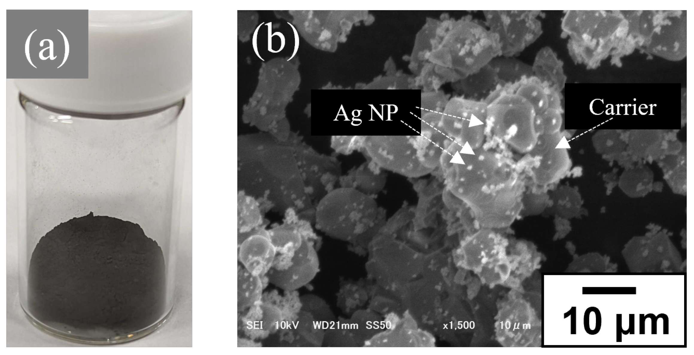
Figure 1a shows the developer consisting of Ag nanoparticles (NPs) and carrier particles [85,86]. The carrier particle comprises the ferrite material and has a role in generating electrical charge in the toner particle by frictional charging and by prohibiting natural aggregation of the toner particle. Industrial carrier particles include a surface polymer layer to adjust frictional charging toward the document-printing toner, although the carrier particles we used had no surface polymer coating. Toner particles mixed with the carrier particles remain on the surface of the carrier particle due to van der Waals forces as well as to the image force between the charged particle and the conductive surface, as mentioned in ref. [86]. The carrier particles were provided by Powdertech Co., Ltd., Tokyo, Japan All carrier particles used in this study were the same. The Ag nanoparticles were purchased from Sigma-Aldrich (Burlington, MA, USA) and were used as received. The carrier particles and Ag nanoparticles were mixed to form the developer. The dark gray particles include approximately 10% Ag NPs and 90% carrier particles by weight, and the mixed powder had sufficient fluidity for the developer particles. The fluidity of the developer particles is essential for drawing high-resolution electronic circuits, which are evaluated using the repose angle [85]. Figure 1b shows the SEM image of the developer. The Ag NP toner particles were distributed on the surfaces of the carrier particles. In these appropriately mixed particles, the natural aggregation of Ag NPs was effectively prevented. Consequently, the Ag NPs maintained sub-micrometer particle diameters.
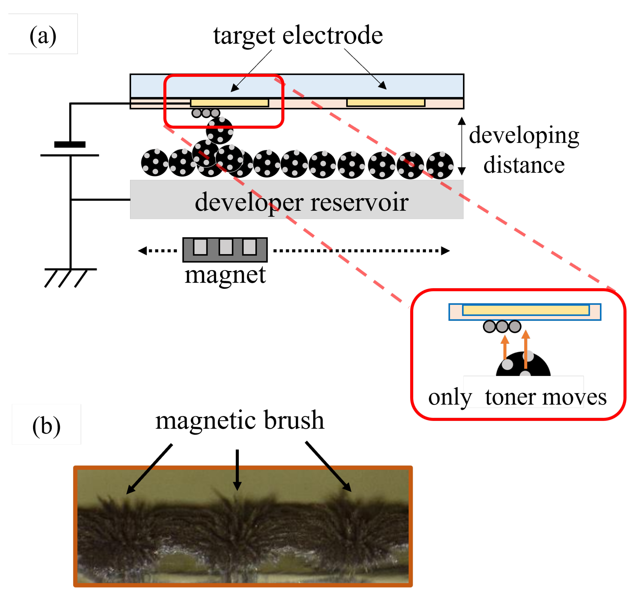
Figure 2a shows a schematic of the electrophotographic printing equipment. The development system comprised a target electrode, developer reservoir, external voltage supply, and a motorized moving magnet. The developer above the magnet forms a brush-like structure along the magnetic lines of force called a magnetic brush. Figure 2b presents a photograph of a magnetic brush. As shown in the figure, magnetic brushes were formed above each magnet. A motorized mechanism drives the reciprocal motion of the magnetic brush along the developer reservoir. Therefore, the tip of the magnetic brush skims the surface of the insulation layer of the target electrode substrate. In this situation, an external voltage is applied between the developer reservoir and target electrode. Subsequently, the charged toner particles of the electronic materials move from the carrier particle surface toward the target electrodes along the electric lines of force and develop images of the electrical circuits and devices. In contrast, the carrier particles remain in the developer reservoir because they are attracted by a strong magnetic field. Only the toner particles of the electronic materials are transferred onto the surface of the target electrode substrate to form an image of the device components, such as interdigital source/drain electrodes of thin-film transistors, semiconductor layers, and gate insulator layers.
The developed image was then transferred from the substrate to a plastic film. Currently, we have adopted an adhesive layer-based transfer method, although there are many alternatives. A thin polyethylene terephthalate (PET) film substrate with a thin and weak adhesive layer was prepared, and the PET film was laminated onto the target electrode substrate. After the PET film was delaminated from the target electrode substrate, toner images were transferred onto the PET film surface. This method is useful in the prototyping stage because the thin adhesive layer inhibits the slipping of the PET film during the transfer process, and it is easy to finish the device as a laminated device, which is expected to be durable in bending and surface scratches and to prevent surface contamination of the device, such as airborne particles and water drops.
IPL sintering [88,89,90,91,92,93,94,95,96,97,98] was performed after the developed patterns were transferred. A commercially distributed xenon flash lamp was used as the IPL light source. The main component of xenon flash lamp radiation is visible light, including near-infrared region light. In our light source, the UV region was cut using an optical filter. Because the PET film was transparent to visible light, only the toner patterns developed were sintered via IPL without damaging the PET film. The instantaneous maximum temperature is not easily estimated and depends on the materials and surface; however, some vaporized particles were observed around the printed pattern when the Zn toner pattern was IPL sintered; therefore, the instantaneous maximum temperature was estimated to be over the boiling point of Zn (approximately 907 °C). After the IPL sintering, two-terminal, four-probe electrical resistance measurements were performed using a 34420A nanovoltmeter (Keysight Technologies, Santa Clara, CA, USA).
3. Results and Discussion
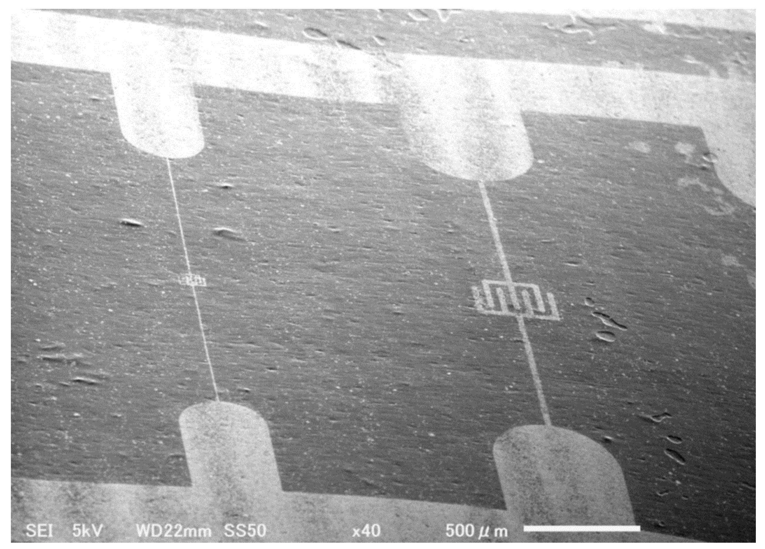
Figure 3 displays an SEM image of the printed microcircuit pattern obtained via toner printing. The bright pattern comprises Ag–Ni conductive particles, and the dark background corresponds to the carbon tape used for SEM observation. The Ag–Ni pattern was directly transferred from the developed substrate surface to the carbon tape surface. The right side of the SEM micrograph shows an Ag–Ni interdigital electrode pattern with a linewidth of 30 m, and the left side shows a 10 m linewidth interdigital electrode pattern printed using the electrophotography method. The 30 m linewidth interdigital electrode patterns show a precise contour similar to their designed original shape and comprise sufficiently uniform and dense Ag–Ni particles that can be used as electrode patterns in microelectronic circuits. The 10 m linewidth pattern also exhibits a clear shape, as originally designed; however, the contour of the 10 m linewidth pattern is slightly jagged. The success rate of printing 5 m linewidth interdigital electrode patterns is currently relatively low and depends on the material, i.e., the particle diameter and fluidity of the powder. Among the present toner particles, Ag–Ni and indium tin oxide (ITO) are suitable for the 5 m pattern.
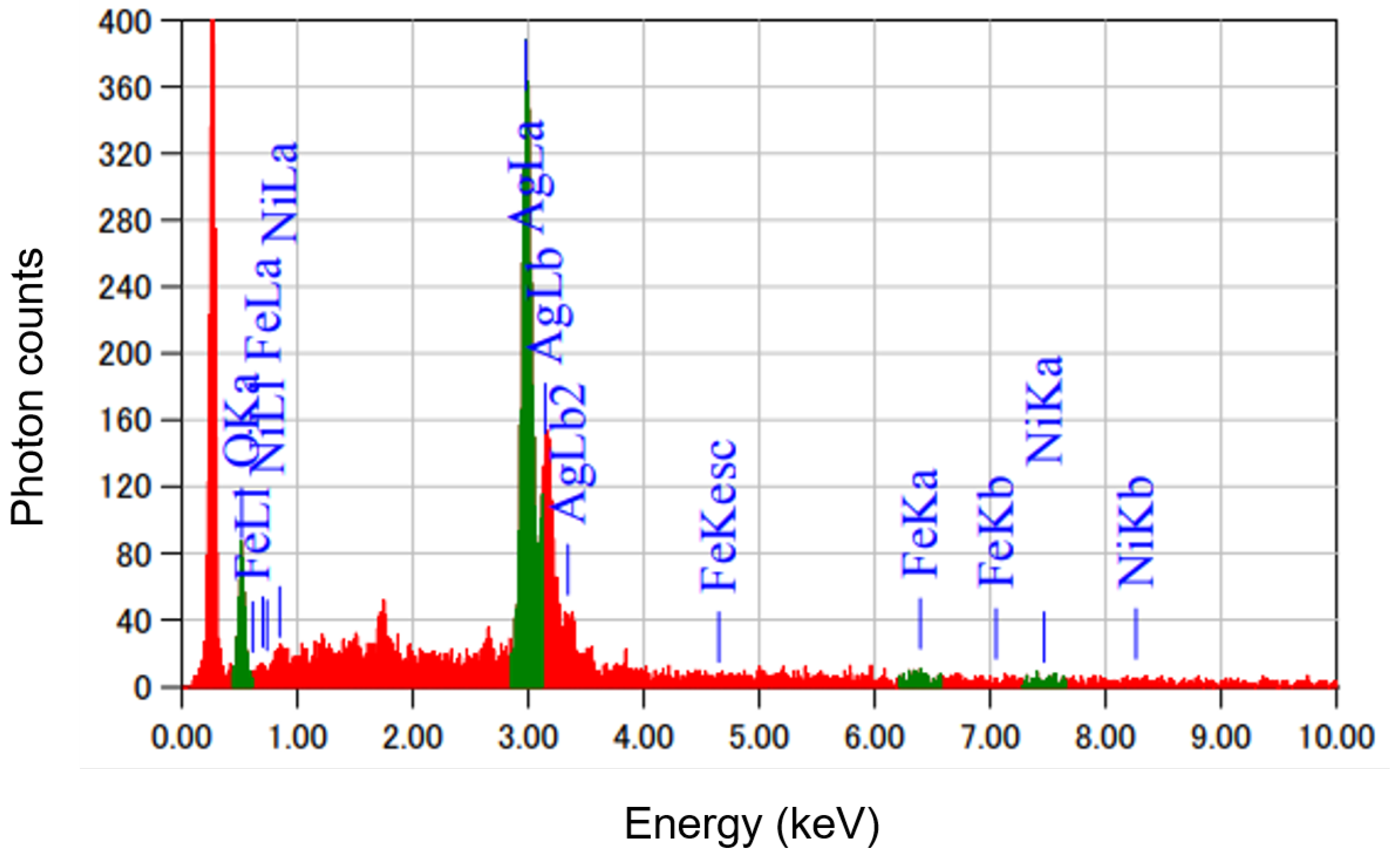
The energy dispersive X-ray (EDX) spectrum of the printed Ag–Ni toner pattern transferred to the surface of the carbon tape is provided in Figure 4. Characteristic X-ray lines of Ag, Ni, Fe, C, and O can be observed from the Ag–Ni toner pattern surface. Ag lines appear at approximately 3 keV as the main peak, and slight Fe and Ni lines are apparent at approximately the 6.3 and 7.5 keV regions, respectively. Owing to the atomic ratio calculation, excluding O and C, 94% Ag, 1.8% Ni, and 3.6% Fe were estimated. As the nominal mixing atomic ratio of Ag:Ni was 5.44:1, the expected Ni ratio was 15.5%. However, the Ni atomic ratio in the printed Ag–Ni pattern was remarkably lower than the nominal ratio. This is because the magnetic field attracts excess Ni nanoparticles that remain in the developer’s powder. Consequently, the purity of Ag in the printed Ag pattern becomes higher than that in the nominal pattern, which effectively prevents an increase in the electrical resistivity, regardless of the addition of Ni nanoparticles. Therefore, the Ni addition effectively improved the fluidity of the Ag toner particles and did not degrade the electrical conductance of the printed Ag pattern. In addition, the slight amount of Fe detected by EDX can be attributed to small fragments of the carrier particles. The weight ratio of the Fe components is less than 1%. However, a higher Ag ratio is crucial for approaching the lower limit of electrical resistivity.
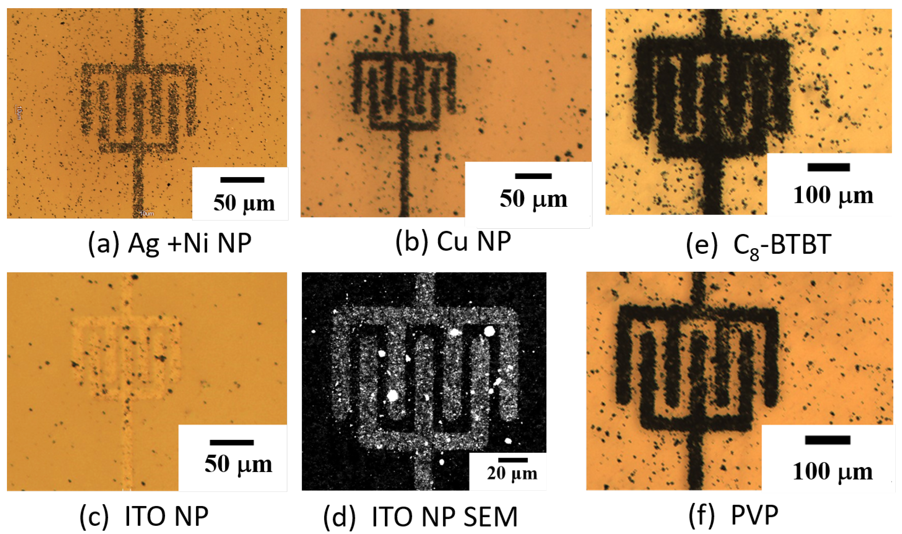
Figure 5 shows the optical micrographs of the printed micro-interdigital electrode pattern obtained using various electronic materials. Ag–Ni in Figure 5a and Cu NPs in Figure 5b appear comparable. Ni NP-added Ag NPs are superior to Ag NPs in terms of fluidity [85]. Therefore, the results printed with Ag–Ni NPs are more precise and stable, particularly in high-resolution printing. Cu NPs in Figure 5b and Zn NPs also show a 10 m linewidth scale resolution. The Cu and Zn NPs exhibited high fluidity, probably because of surface oxidation of Cu and Zn. However, Au particles have a highly active surface; therefore, they spontaneously grow into larger particles over time by taking the surrounding Au particles onto their surface. More specifically, Au nanoparticles cannot exist as dried nanoparticles. In contrast, Au solution inks contain chemical agents that separate the Au particles; therefore, they do not directly contact the Au surfaces in the solution. Consequently, creating a high-resolution (10 m scale) Au pattern using electrophotographic printing is currently difficult, although macro-scale Au circuit printing is possible.
In addition, the main components of the small scattered particles around the printed interdigital pattern are stray toner particles and aggregates. Because some of the low-charged toner particles tend to scatter owing to the movement of the magnetic brush during the printing process, a small number of toner particles stick to the target electrode substrate surface. It is necessary to decrease the toner ratio of the developer to reduce excess toner scattering. A minor component of the scattered particles is a fragment of the carrier particles. Large fragments of carrier particles were removed using a magnet. However, smaller carrier particle fragments have lower magnetic attractive force owing to their smaller volume and are thus difficult to remove. Methods for suppressing or removing particles of small size have yet to be fully developed.
Graphene nanoplatelets (GNPs) purchased from Aldrich were expected to be conductive electronic materials that could be developed using electrophotographic printing. The nominal size of the GNP was less than 2 m in diameter and a few nanometers in thickness. GNPs are excellent electronic toner materials because of their high fluidity and sufficiently small particle sizes, producing several m patterns. In addition, the electrical resistance of the developed GNPs was sufficiently low, even before the sintering process. In addition, it was confirmed that carbon nanotube powder and other carbon material particles were also developed using the electrophotographic method. Therefore, by combining the proper sintering processes, thin-film printing of carbon materials is possible. These materials could be useful in the development of batteries.
Oxide electronic materials such as ITO, ZnO, NiO, and SiO2 NPs can also be printed using electrophotography. All oxide powders were purchased from Sigma-Aldrich (Burlington, MA, USA) and were used as received. Figure 5c shows the results of high-resolution ITO printing. Because ITO is a transparent electrode material, it is difficult to observe the developed ITO pattern under optical observation conditions. However, a high-resolution interdigital electrode pattern was formed and confirmed via SEM observations (Figure 5d). The SEM result shows that the developed ITO NP pattern was clear-cut and had a dense and uniform distribution. Oxide electronic materials, including ITO, ZnO, and NiO, also have relatively high fluidity and do not spontaneously form aggregates; therefore, they are advantageous for high-resolution electrophotographic printing. These oxide electronic materials are also beneficial for dense and thick pattern formation owing to their low density and high electrical charge. Thus, such materials are useful for fabricating transparent electronics.
Organic electronic materials, including C8-BTBT, Poly(4-vinylphenol) (PVP), PSS-Octakis (dimethylsilyloxy), and PSS-(2-(trans-3,4-Cyclohexanediol) ethyl)-heptaisobutyl substituted (PSSs), can be electrophotographically printed, as shown in Figure 5e,f. Figure 5e displays the printed C8-BTBT toner pattern. The C8-BTBT is an organic semiconductor. In the initial stage of this study, we could only obtain a sparse pattern of C8-BTBT [86]; however, we can now create a sufficiently dense pattern of C8-BTBT toner particles. A small number of C8-BTBT toner particles was sufficient to fabricate a thin-film transistor because the volume of the toner particles was sufficient to fill a thin layer of less than several dozen nm [86]. PVP is a polymeric insulator material expected to act as a gate insulator in organic thin-film transistors. The melting point of PVP is 360 °C, which may be too high to fix PVP particles on the PET film thermally. PSS group polymers are alternative insulating polymers, with melting points ranging from 120 °C to 350°C. However, as the melting point decreases, ball milling of these materials becomes difficult, the fluidity of nano/micro-particles decreases. Their fluidity can be adjusted with the addition of inert nanoparticles, including SiO2 NPs.
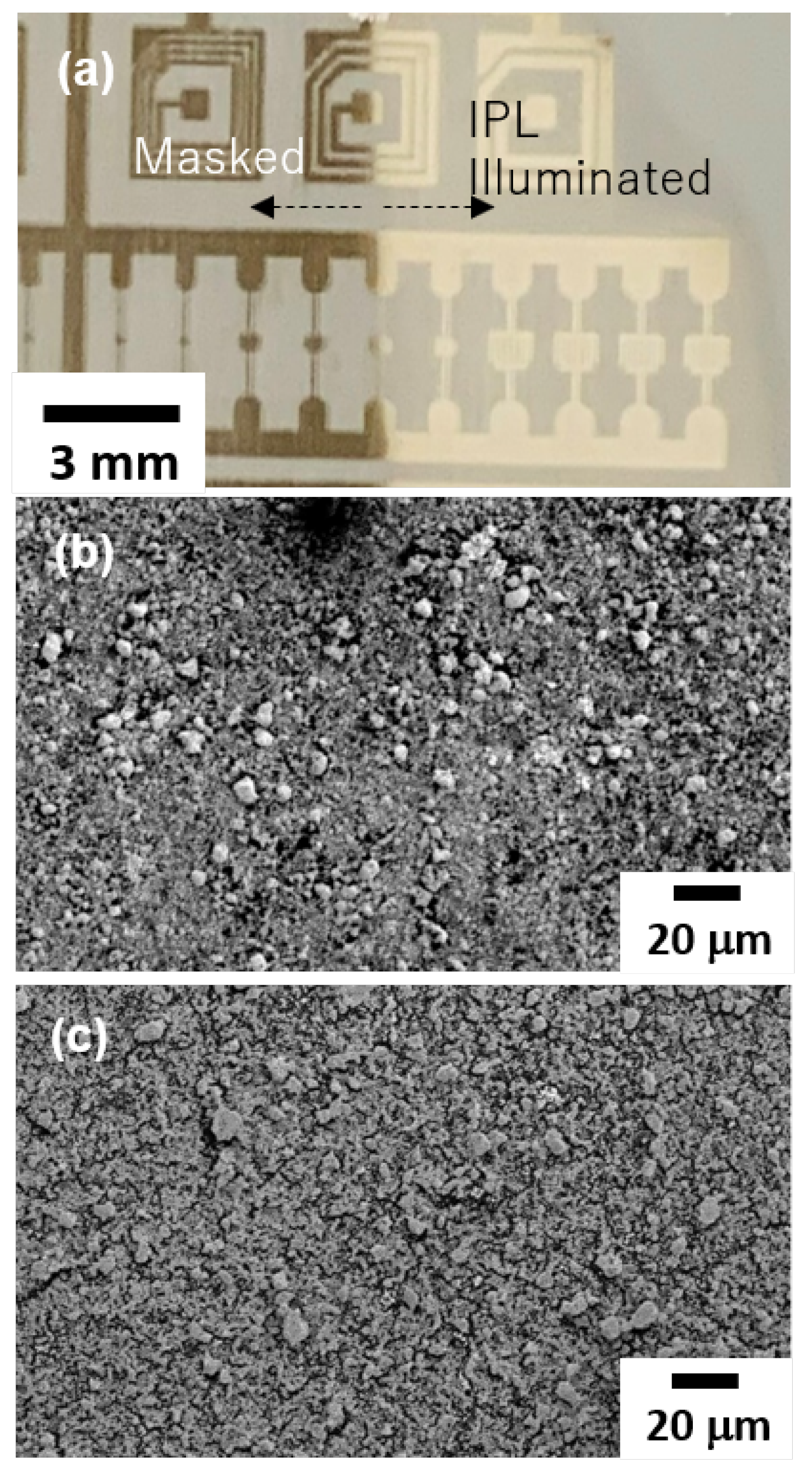
After the electrophotographic development of the electronic materials, the materials had to be fixed because the toner particles are individual, not forming a thin film. As previously investigated, materials with lower melting points, such as organic semiconductors, can be thermally fixed [86,99,100]. Application of ultrasonic vibration produces a thermal effect that is also useful for melting the organic semiconductor [87], as well as a mechanical effect that is effective for fixing metals such as Au and Ag. In this study, IPL sintering was performed to sinter metallic materials. Figure 6a shows the printed Ag stripe patterns before and after IPL sintering. The left half of the figure shows the powdery Ag pattern on the PET film, and the right half shows the IPL applied region. Before sintering, the surface of the printed Ag stripe exhibited a dark gray color and no gloss. Conversely, the IPL applied surface has a white-silver color and is glossy, specific to the bulk Ag surface. This change in appearance is achieved after applying several pulsed light flashes. SEM micrographs of the printed Ag pattern surfaces before and after IPL sintering are displayed in Figure 6b,c, respectively. The surface of the developed Ag stripe comprised individual Ag particles densely packed within the stripe pattern. However, after IPL sintering, the boundaries of the Ag particles became unclear because the surfaces of the Ag nanoparticles melted slightly and formed connections with them. No individual particles are observed on the IPL-sintered surface in the SEM images, and the features of the original piled particles are retained. In addition, a glossy silver color was observed in the macroscopic image. This indicates that the developed Ag particles formed continuous Ag thin films after IPL sintering.
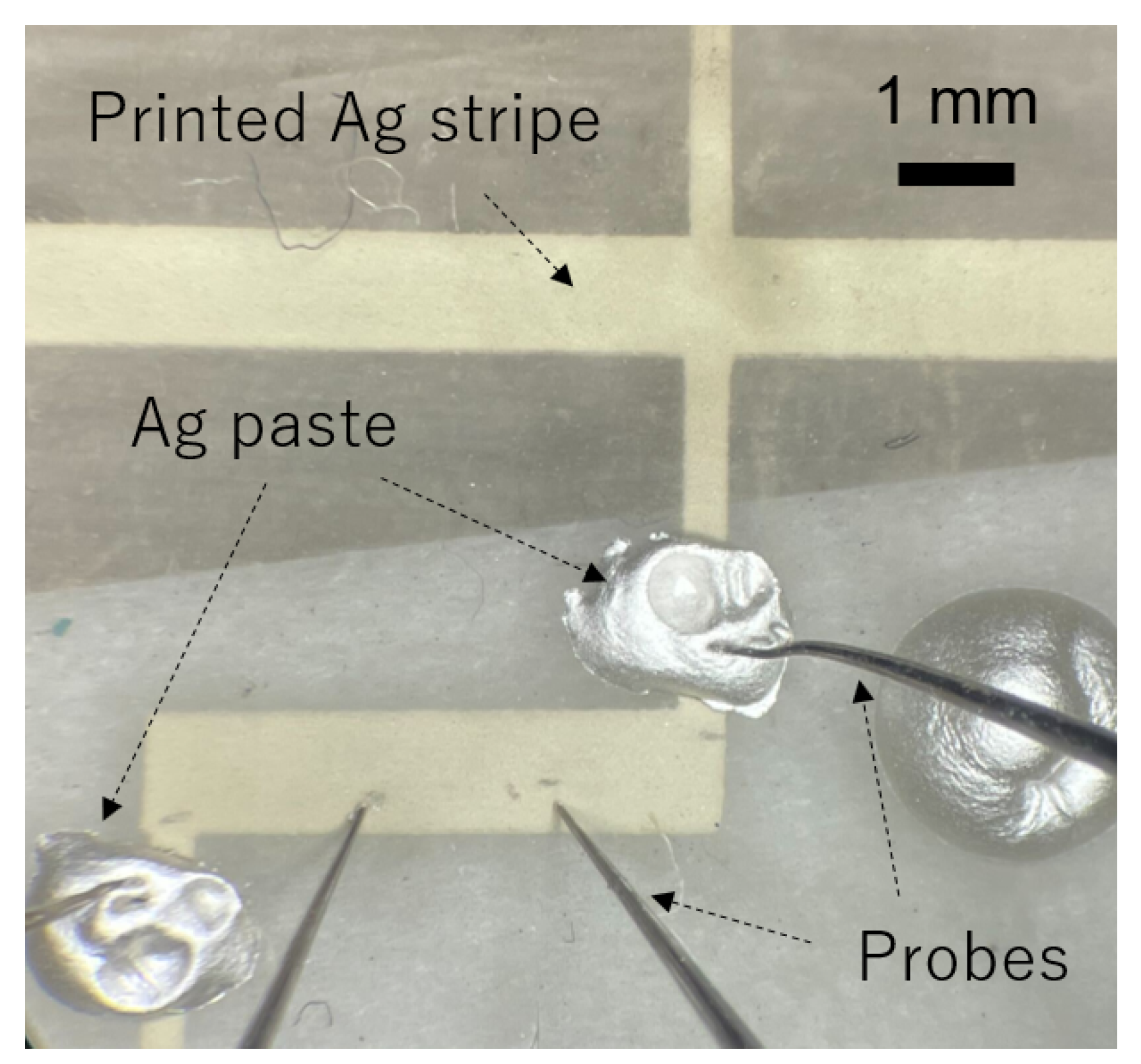
Figure 7 presents the printed Ag–Ni stripe pattern used for the four-probe electrical resistance measurement. A steady electrical current flow was applied between the two Ag paste pads, reinforcing the ohmic electrical contact by securing a sufficient contact area. The two probes touched the Ag paste, and an electrical current flowed through the sample. In addition, two other probes were used to measure the electrical voltage difference by directly touching the sintered Ag–Ni striped surface. Because the printed Ag–Ni stripe is thin, direct contact of the probes with the Ag–Ni stripe surface carries the risk of damaging the stripe. Therefore, we used a contact probe with a tip radius of 50 m to touch the Ag surface carefully. The two-terminal electrical resistance was greater than 75 M before sintering; however, it decreased to 84.9 after IPL sintering. We obtained 3.07 using four-probe electrical-resistance measurements. As a result, the electrical resistivity of the Ag–Ni stripe was 8.96 × 10⁻⁶m. This is presently higher than the recent electrical resistivity reported using Ag nanoparticles (ranging from 3.9 × 10⁻⁸m to 2.4 × 10⁻⁴m) [101,102,103,104,105] and Ag nanowires (ranging from 3.6 × 10⁻⁸m to 2.6 × 10⁻⁶m) [71,106,107,108,109]. The highest measurements are very close to the electrical resistivity of bulk Ag; however, wide applications in the electrical engineering field are expected even if the electrical resistivity is not comparable to the world champion data. The typical electrical resistivity values of commercially available Ag paste and ITO thin films are approximately 10−7m and 10−6m, respectively. The electrical resistivity of the sintered Ag–Ni stripes was nearly equivalent to that of commercial ITO thin films. However, this Ag–Ni conductive thin film does not require vacuum processes such as sputtering or thermal annealing and is instantly sintered by several IPL pulses. In addition, the effect of the light pulse on the metallic material is maximal at the surface and rapidly decreases in the depth direction; therefore, a thick Ag–Ni film is disadvantageous in terms of the average electrical resistivity under limited IPL pulse intensity. More specifically, the local electrical resistivity around the Ag–Ni stripe surface is expected to be lower than the present average electrical resistivity of 8.96 × 10⁻⁶m. Therefore, there is room for improvement in the electrical resistivity of the printed Ag–Ni stripe under proper IPL sintering conditions.
Although PET film with a weak adhesive layer was used in this study, we mention the possibility of direct printing onto other substrates such as PET or paper surfaces. Toner particles developed on the appropriate substrate keep electrical charges. Therefore, we can transfer the developed Ag patterns by applying a reverse voltage to release the toner particles from the target electrode substrate surface and transfer them to another substrate. In addition, if there is no electrical charge in the printed toner particles, applying only the appropriate pressure is sufficient to pick up the toner nanoparticles. Because the adsorption force between the toner particle and the substrate surface differs depending on the substrate material, such as PET, polyimide, or cellulose (paper), the combination and selection of materials is important. The use of an adhesive layer on the substrate is another effective measure, as indicated in this study.
4. Conclusions
We established high-resolution electrophotographic printing of various electronic materials, including metals, carbon and oxide conductors, oxide and organic semiconductors, and insulators. The present printing resolution was 10 m; however, a 5 m line and space are possible depending on the material, i.e., the effective diameter and fluidity of the powder. IPL sintering was effective in fixing the printed powdery metal pattern and finishing it as a low-resistance electrical circuit pattern. The electrical resistivity obtained is comparable to that of a commercial ITO thin film. Because the Ag toner is a bare metal particle that is free from additional chemical agents, thermal annealing to burn the chemicals is unnecessary, and several IPL pulses are sufficient to convert the powdery metal pattern into a thin film. Therefore, electrophotographic printed electronics can save materials, energy, and processing time.
Author Contributions
Formal analysis and investigation: C.Y.N., K.K. (Kaito Kozuki), H.O., S.B.L., R.H. and S.K.; resources: S.K.; Writing—original draft preparation: M.S. and C.Y.N.; writing—review and editing: M.S., C.Y.N. and K.K. (Kazuhiro Kudo); funding acquisition: M.S. All authors have read and agreed to the published version of the manuscript.
Funding
This research was funded by a grant from the A-STEP program of the Japan Science and Technology Agency (Grant# JPMJTM22B3).
Institutional Review Board Statement
Not applicable.
Informed Consent Statement
Not applicable.
Data Availability Statement
The data presented in this study are available on request from the corresponding author.
Acknowledgments
The authors thank T. Sawada of the RICHO Company, Ltd. The authors also thank F. Sawamura for technical advice and experimental contributions. Carrier particles were provided by Powdertech Co., Ltd.
Conflicts of Interest
The authors declare no conflicts of interest. The funders had no role in the study design, collection, analyses, interpretation of data, writing of the manuscript, or the decision to publish the results.
References
- Khan, Y.; Thielens, A.; Muin, S.; Ting, J.; Baumbauer, C.; Arias, A.C. A new frontier of printed electronics: Flexible hybrid electronics. Adv. Mater. 2020, 32, 1905279. [Google Scholar] [CrossRef] [PubMed]
- Tan, H.W.; Choong, Y.Y.C.; Kuo, C.N.; Low, H.Y.; Chua, C.K. 3D printed electronics: Processes, materials and future trends. Prog. Mater. Sci. 2022, 127, 100945. [Google Scholar] [CrossRef]
- Bonnassieux, Y.; Brabec, C.J.; Cao, Y.; Carmichael, T.B.; Chabinyc, M.L.; Cheng, K.T.; Cho, G.; Chung, A.; Cobb, C.L.; Distler, A.; et al. The 2021 flexible and printed electronics roadmap. Flex. Print. Electron. 2021, 6, 023001. [Google Scholar] [CrossRef]
- Wiklund, J.; Karakoç, A.; Palko, T.; Yiğitler, H.; Ruttik, K.; Jäntti, R.; Paltakari, J. A review on printed electronics: Fabrication methods, inks, substrates, applications and environmental impacts. J. Manuf. Mater. Process. 2021, 5, 89. [Google Scholar] [CrossRef]
- Dahiya, A.S.; Shakthivel, D.; Kumaresan, Y.; Zumeit, A.; Christou, A.; Dahiya, R. High-performance printed electronics based on inorganic semiconducting nano to chip scale structures. Nano Converg. 2020, 7, 33. [Google Scholar] [CrossRef] [PubMed]
- Kamyshny, A.; Magdassi, S. Conductive nanomaterials for printed electronics. Small 2014, 10, 3515–3535. [Google Scholar] [CrossRef] [PubMed]
- Garlapati, S.K.; Divya, M.; Breitung, B.; Kruk, R.; Hahn, H.; Dasgupta, S. Printed electronics based on inorganic semiconductors: From processes and materials to devices. Adv. Mater. 2018, 30, 1707600. [Google Scholar] [CrossRef]
- Kunnari, E.; Valkama, J.; Keskinen, M.; Mansikkamäki, P. Environmental evaluation of new technology: Printed electronics case study. J. Clean. Prod. 2009, 17, 791–799. [Google Scholar] [CrossRef]
- Chang, J.S.; Facchetti, A.F.; Reuss, R. A circuits and systems perspective of organic/printed electronics: Review, challenges, and contemporary and emerging design approaches. IEEE J. Emerg. Sel. Top. Circuits Syst. 2017, 7, 7–26. [Google Scholar] [CrossRef]
- Cano-Raya, C.; Denchev, Z.Z.; Cruz, S.F.; Viana, J.C. Chemistry of solid metal-based inks and pastes for printed electronics—A review. Appl. Mater. Today 2019, 15, 416–430. [Google Scholar] [CrossRef]
- Berggren, M.; Nilsson, D.; Robinson, N.D. Organic materials for printed electronics. Nat. Mater. 2007, 6, 3–5. [Google Scholar] [CrossRef] [PubMed]
- Leenen, M.A.; Arning, V.; Thiem, H.; Steiger, J.; Anselmann, R. Printable electronics: Flexibility for the future. Phys. Status Solidi A 2009, 206, 588–597. [Google Scholar] [CrossRef]
- Lewis, J.A.; Ahn, B.Y. Three-dimensional printed electronics. Nature 2015, 518, 42–43. [Google Scholar] [CrossRef] [PubMed]
- Hoeng, F.; Denneulin, A.; Bras, J. Use of nanocellulose in printed electronics: A review. Nanoscale 2016, 8, 13131–13154. [Google Scholar] [CrossRef] [PubMed]
- Zeng, X.; He, P.; Hu, M.; Zhao, W.; Chen, H.; Liu, L.; Sun, J.; Yang, J. Copper inks for printed electronics: A review. Nanoscale 2022, 14, 16003–16032. [Google Scholar] [CrossRef] [PubMed]
- Grau, G.; Cen, J.; Kang, H.; Kitsomboonloha, R.; Scheideler, W.J.; Subramanian, V. Gravure-printed electronics: Recent progress in tooling development, understanding of printing physics, and realization of printed devices. Flex. Print. Electron. 2016, 1, 023002. [Google Scholar] [CrossRef]
- Tiara, A.; Moon, H.; Cho, G.; Lee, J. Fully roll-to-roll gravure printed electronics: Challenges and the way to integrating logic gates. Jpn. J. Appl. Phys. 2022, 61, SE0802. [Google Scholar]
- Chen, S.; Pua, S.; Zhong, Z.; Shan, X. Investigation of Roll-to-Roll Gravure Printing for Printed Electronics with Fine Features. J. Mater. Appl. 2020, 9, 79–89. [Google Scholar] [CrossRef]
- Lee, S.H.; Lee, S. Fabrication of comb-structured acceleration sensors by roll-to-roll gravure printing. Int. J. Precis. Eng. Manuf.-Green Technol. 2022, 9, 409–420. [Google Scholar] [CrossRef]
- Jo, M.; Lee, J.; Kim, S.; Cho, G.; Lee, T.M.; Lee, C. Resistance control of an additively manufactured conductive layer in roll-to-roll gravure printing systems. Int. J. Precis. Eng. Manuf.-Green Technol. 2021, 8, 817–828. [Google Scholar] [CrossRef]
- Park, J.; Shrestha, S.; Parajuli, S.; Jung, Y.; Cho, G. Fully roll-to-roll gravure printed 4-bit code generator based on p-type SWCNT thin-film transistors. Flex. Print. Electron. 2021, 6, 044005. [Google Scholar] [CrossRef]
- Peng, M.; Wang, Y.; Wu, M.; Wu, S.; Chai, C.; Xue, Z. Simulation and Experimental Research on the Effect of Scraper Pressure on Pattern Transferring Process of Gravure Printed Electronic Equipment. J. Imaging Sci. Technol. 2023, 67, 1. [Google Scholar] [CrossRef]
- Choi, Y.; Jung, Y.; Song, R.; Park, J.; Parajuli, S.; Shrestha, S.; Cho, G.; Kim, B.S. Rapid Uniformity Analysis of Fully Printed SWCNT-Based Thin Film Transistor Arrays via Roll-to-Roll Gravure Process. Nanomaterials 2023, 13, 590. [Google Scholar] [CrossRef]
- Lee, J.; Kim, J.; Noh, Y.; Jeong, H.; Lee, D. Advanced technique for achieving 10-μm-width fine lines in roll-to-roll continuous gravure printing. Precis. Eng. 2021, 69, 1–7. [Google Scholar] [CrossRef]
- Zhang, Q.; Ren, Y.; Wang, Z.; Chen, X.; Portilla, L.; Sun, L.; Zhang, D.; Zhao, J. Preparation of large-area, high-performance single-walled carbon nanotube (SWCNT)-based heater films by roll-to-roll gravure printing. Flex. Print. Electron. 2022, 7, 015007. [Google Scholar] [CrossRef]
- Fakhari, A.; Fernandes, C.; Galindo-Rosales, F.J. Mapping the volume transfer of graphene-based inks with the gravure printing process: Influence of rheology and printing parameters. Materials 2022, 15, 2580. [Google Scholar] [CrossRef]
- Yang, L.; Tong, S.; Gong, C.; Xia, H.; Wang, C.; Liu, B.; Liu, B.; Xie, H.; Xiao, S.; He, J.; et al. Large-scale roll-to-roll micro-gravure printed flexible PBDB-T/IT-M bulk heterojunction photodetectors. Appl. Phys. A 2020, 126, 442. [Google Scholar] [CrossRef]
- Zavanelli, N.; Yeo, W.H. Advances in screen printing of conductive nanomaterials for stretchable electronics. ACS Omega 2021, 6, 9344–9351. [Google Scholar] [CrossRef]
- Brooke, R.; Wijeratne, K.; Hübscher, K.; Belaineh, D.; Andersson Ersman, P. Combining vapor phase polymerization and screen printing for printed electronics on flexible substrates. Adv. Mater. Technol. 2022, 7, 2101665. [Google Scholar] [CrossRef]
- Gafurov, A.N.; Jeong, J.; Park, P.; Kim, I.; Phung, T.H.; Kim, H.C.; Kang, D.; Oh, D.; Lee, T.M. Registration error analysis and compensation of roll-to-roll screen printing system for flexible electronics. Flex. Print. Electron. 2021, 6, 024003. [Google Scholar] [CrossRef]
- Liu, L.; Shen, Z.; Zhang, X.; Ma, H. Highly conductive graphene/carbon black screen printing inks for flexible electronics. J. Colloid Interface Sci. 2021, 582, 12–21. [Google Scholar] [CrossRef] [PubMed]
- Zhang, Y.; Zhu, Y.; Zheng, S.; Zhang, L.; Shi, X.; He, J.; Chou, X.; Wu, Z.S. Ink formulation, scalable applications and challenging perspectives of screen printing for emerging printed microelectronics. J. Energy Chem. 2021, 63, 498–513. [Google Scholar] [CrossRef]
- Andersson Ersman, P.; Lassnig, R.; Strandberg, J.; Dyreklev, P. Flexible active matrix addressed displays manufactured by screen printing. Adv. Eng. Mater. 2021, 23, 2000771. [Google Scholar] [CrossRef]
- Li, W.; Zhang, H.; Kagita, S.; Shamim, A. All Screen-Printed, Polymer-Nanowire Based Foldable Electronics for mm-Wave Applications. Adv. Mater. Technol. 2021, 6, 2100525. [Google Scholar] [CrossRef]
- Altay, B.N.; Turkani, V.S.; Pekarovicova, A.; Fleming, P.D.; Atashbar, M.Z.; Bolduc, M.; Cloutier, S.G. One-step photonic curing of screen-printed conductive Ni flake electrodes for use in flexible electronics. Sci. Rep. 2021, 11, 3393. [Google Scholar] [CrossRef]
- Li, W.; Vaseem, M.; Yang, S.; Shamim, A. Flexible and reconfigurable radio frequency electronics realized by high-throughput screen printing of vanadium dioxide switches. Microsyst. Nanoeng. 2020, 6, 77. [Google Scholar] [CrossRef]
- Qi, X.; Ha, H.; Hwang, B.; Lim, S. Printability of the screen-printed strain sensor with carbon black/silver paste for sensitive wearable electronics. Appl. Sci. 2020, 10, 6983. [Google Scholar] [CrossRef]
- Gong, X.; Huang, K.; Wu, Y.H.; Zhang, X.S. Recent progress on screen-printed flexible sensors for human health monitoring. Sens. Actuators A Phys. 2022, 345, 113821. [Google Scholar] [CrossRef]
- Hong, H.; Jiang, L.; Tu, H.; Hu, J.; Yan, X. Formulation of UV curable nano-silver conductive ink for direct screen-printing on common fabric substrates for wearable electronic applications. Smart Mater. Struct. 2021, 30, 045001. [Google Scholar] [CrossRef]
- Suresh, R.R.; Lakshmanakumar, M.; Arockia Jayalatha, J.; Rajan, K.; Sethuraman, S.; Krishnan, U.M.; Rayappan, J.B.B. Fabrication of screen-printed electrodes: Opportunities and challenges. J. Mater. Sci. 2021, 56, 8951–9006. [Google Scholar] [CrossRef]
- Sopeña, P.; Fernández-Pradas, J.; Serra, P. Laser-induced forward transfer of conductive screen-printing inks. Appl. Surf. Sci. 2020, 507, 145047. [Google Scholar] [CrossRef]
- Linderhed, U.; Petsagkourakis, I.; Ersman, P.A.; Beni, V.; Tybrandt, K. Fully screen printed stretchable electrochromic displays. Flex. Print. Electron. 2021, 6, 045014. [Google Scholar] [CrossRef]
- Kim, S. Inkjet-printed electronics on paper for RF identification (RFID) and sensing. Electronics 2020, 9, 1636. [Google Scholar] [CrossRef]
- Song, O.; Rhee, D.; Kim, J.; Jeon, Y.; Mazánek, V.; Söll, A.; Kwon, Y.A.; Cho, J.H.; Kim, Y.H.; Sofer, Z.; et al. All inkjet-printed electronics based on electrochemically exfoliated two-dimensional metal, semiconductor, and dielectric. NPJ 2D Mater. Appl. 2022, 6, 64. [Google Scholar] [CrossRef]
- Beedasy, V.; Smith, P.J. Printed electronics as prepared by inkjet printing. Materials 2020, 13, 704. [Google Scholar] [CrossRef]
- Roach, D.J.; Roberts, C.; Wong, J.; Kuang, X.; Kovitz, J.; Zhang, Q.; Spence, T.G.; Qi, H.J. Surface modification of fused filament fabrication (FFF) 3D printed substrates by inkjet printing polyimide for printed electronics. Addit. Manuf. 2020, 36, 101544. [Google Scholar] [CrossRef]
- Yan, K.; Li, J.; Pan, L.; Shi, Y. Inkjet printing for flexible and wearable electronics. APL Mater. 2020, 8, 120705. [Google Scholar] [CrossRef]
- Tilford, T.; Stoyanov, S.; Braun, J.; Janhsen, J.C.; Patel, M.K.; Bailey, C. Comparative reliability of inkjet-printed electronics packaging. IEEE Trans. Components Packag. Manuf. Technol. 2021, 11, 351–362. [Google Scholar] [CrossRef]
- Zhu, D.; Wang, Z.; Zhu, D. Highly conductive graphene electronics by inkjet printing. J. Electron. Mater. 2020, 49, 1765–1776. [Google Scholar] [CrossRef]
- Pinto, R.M.; Nemala, S.S.; Faraji, M.; Capasso, A.; Vinayakumar, K. Inkjet-Printing of Carbon Nano Onions for Sensor Applications in Flexible Printed Electronics. In Proceedings of the 2022 IEEE International Conference on Flexible and Printable Sensors and Systems (FLEPS), Vienna, Austria, 10–13 July 2022; pp. 1–4. [Google Scholar]
- Sun, B.; Liu, Y.; Zhu, H.; Xing, L.; Bu, Q.; Ren, D. Recent advances of inkjet-printing technologies for flexible/wearable electronics. Nanoscale 2023, 15, 6025–6051. [Google Scholar]
- Schlisske, S.; Raths, S.; Ruiz-Preciado, L.A.; Lemmer, U.; Exner, K.; Hernandez-Sosa, G. Surface energy patterning for ink-independent process optimization of inkjet-printed electronics. Flex. Print. Electron. 2021, 6, 015002. [Google Scholar] [CrossRef]
- Kathirvelan, J. Recent developments of inkjet-printed flexible sensing electronics for wearable device applications: A review. Sens. Rev. 2021, 41, 46–56. [Google Scholar] [CrossRef]
- Rauter, L.; Zikulnig, J.; Sinani, T.; Zangl, H.; Faller, L.M. Evaluation of standard electrical bonding strategies for the hybrid integration of inkjet-printed electronics. Electron. Mater. 2020, 1, 2–16. [Google Scholar] [CrossRef]
- Tarabella, G.; Vurro, D.; Lai, S.; D’Angelo, P.; Ascari, L.; Iannotta, S. Aerosol jet printing of PEDOT: PSS for large area flexible electronics. Flex. Print. Electron. 2020, 5, 014005. [Google Scholar] [CrossRef]
- Kim, B. Inkjet-printed ternary inverter circuits with tunable middle logic voltages. Adv. Electron. Mater. 2020, 6, 2000426. [Google Scholar] [CrossRef]
- Zhuo, L.; Liu, W.; Zhao, Z.; Yin, E.; Li, C.; Zhou, L.; Zhang, Q.; Feng, Y.; Lin, S. Cost-effective silver nano-ink for inkjet printing in application of flexible electronic devices. Chem. Phys. Lett. 2020, 757, 137904. [Google Scholar] [CrossRef]
- Labiano, I.I.; Alomainy, A. Flexible inkjet-printed graphene antenna on Kapton. Flex. Print. Electron. 2021, 6, 025010. [Google Scholar] [CrossRef]
- Mohd Asri, M.A.; Ramli, N.A.; Nordin, A.N. Electrical performance and reliability assessment of silver inkjet printed circuits on flexible substrates. J. Mater. Sci. Mater. Electron. 2021, 32, 16024–16037. [Google Scholar] [CrossRef]
- Brunetti, I.; Pimpolari, L.; Conti, S.; Worsley, R.; Majee, S.; Polyushkin, D.K.; Paur, M.; Dimaggio, E.; Pennelli, G.; Iannaccone, G.; et al. Inkjet-printed low-dimensional materials-based complementary electronic circuits on paper. NPJ 2D Mater. Appl. 2021, 5, 85. [Google Scholar] [CrossRef]
- Khan, A.; Rahman, K.; Ali, S.; Khan, S.; Wang, B.; Bermak, A. Fabrication of circuits by multi-nozzle electrohydrodynamic inkjet printing for soft wearable electronics. J. Mater. Res. 2021, 36, 3568–3578. [Google Scholar] [CrossRef]
- Lo, L.W.; Shi, H.; Wan, H.; Xu, Z.; Tan, X.; Wang, C. Inkjet-printed soft resistive pressure sensor patch for wearable electronics applications. Adv. Mater. Technol. 2020, 5, 1900717. [Google Scholar] [CrossRef]
- Piatti, E.; Arbab, A.; Galanti, F.; Carey, T.; Anzi, L.; Spurling, D.; Roy, A.; Zhussupbekova, A.; Patel, K.A.; Kim, J.M.; et al. Charge transport mechanisms in inkjet-printed thin-film transistors based on two-dimensional materials. Nat. Electron. 2021, 4, 893–905. [Google Scholar] [CrossRef]
- Ramon, E.; Sowade, E.; Martinez-Domingo, C.; Mitra, K.Y.; Alcalde, A.; Baumann, R.R.; Carrabina, J. Large-scale fabrication of all-inkjet-printed resistors and WORM memories on flexible polymer films with high yield and stability. Flex. Print. Electron. 2021, 6, 015003. [Google Scholar] [CrossRef]
- Kaçar, R.; Serin, R.B.; Uçar, E.; Ülkü, A. A review of high-end display technologies focusing on inkjet printed manufacturing. Mater. Today Commun. 2023, 35, 105534. [Google Scholar] [CrossRef]
- Majee, S.; Karlsson, M.C.; Wojcik, P.J.; Sawatdee, A.; Mulla, M.Y.; Alvi, N.u.H.; Dyreklev, P.; Beni, V.; Nilsson, D. Low temperature chemical sintering of inkjet-printed Zn nanoparticles for highly conductive flexible electronic components. NPJ Flex. Electron. 2021, 5, 14. [Google Scholar] [CrossRef]
- Huang, T.T.; Wu, W. Inkjet-printed wearable nanosystems for self-powered technologies. Adv. Mater. Interfaces 2020, 7, 2000015. [Google Scholar] [CrossRef]
- Mikkonen, R.; Puistola, P.; Jönkkäri, I.; Mäntysalo, M. Inkjet printable polydimethylsiloxane for all-inkjet-printed multilayered soft electrical applications. ACS Appl. Mater. Interfaces 2020, 12, 11990–11997. [Google Scholar] [CrossRef]
- Jun, H.Y.; Lee, E.J.; Ryu, S.O. Synthesis and characterization of copper ink and direct printing of copper patterns by inkjet printing for electronic devices. Curr. Appl. Phys. 2020, 20, 853–861. [Google Scholar] [CrossRef]
- Hu, G.; Yang, L.; Yang, Z.; Wang, Y.; Jin, X.; Dai, J.; Wu, Q.; Liu, S.; Zhu, X.; Wang, X.; et al. A general ink formulation of 2D crystals for wafer-scale inkjet printing. Sci. Adv. 2020, 6, eaba5029. [Google Scholar] [CrossRef]
- Patil, P.; Patil, S.; Kate, P.; Kulkarni, A.A. Inkjet printing of silver nanowires on flexible surfaces and methodologies to improve the conductivity and stability of the printed patterns. Nanoscale Adv. 2021, 3, 240–248. [Google Scholar] [CrossRef]
- Pietsch, M.; Schlisske, S.; Held, M.; Maag, P.; Hernandez-Sosa, G. Stretchable inkjet-printed electronics on mechanically compliant island-bridge architectures covalently bonded to elastomeric substrates. Flex. Print. Electron. 2022, 7, 025007. [Google Scholar] [CrossRef]
- Wu, X.; Wang, S.; Luo, Z.; Lu, J.; Lin, K.; Xie, H.; Wang, Y.; Li, J.Z. Inkjet printing of flexible transparent conductive films with silver nanowires ink. Nanomaterials 2021, 11, 1571. [Google Scholar] [CrossRef]
- Uzun, S.; Schelling, M.; Hantanasirisakul, K.; Mathis, T.S.; Askeland, R.; Dion, G.; Gogotsi, Y. Additive-free aqueous MXene inks for thermal inkjet printing on textiles. Small 2021, 17, 2006376. [Google Scholar] [CrossRef]
- Zhong, Z.W.; Ee, J.; Chen, S.; Shan, X. Parametric investigation of flexographic printing processes for R2R printed electronics. Mater. Manuf. Processes 2020, 35, 564–571. [Google Scholar] [CrossRef]
- Gajadhur, M.; Regulska, M. Mechanical and light resistance of flexographic conductive ink films intended for printed electronics. Dyes Pigments 2020, 178, 108381. [Google Scholar] [CrossRef]
- Morgan, M.L.; Curtis, D.J.; Deganello, D. Control of morphological and electrical properties of flexographic printed electronics through tailored ink rheology. Org. Electron. 2019, 73, 212–218. [Google Scholar] [CrossRef]
- Rodes-Carbonell, A.M.; Ferri, J.; Garcia-Breijo, E.; Montava, I.; Bou-Belda, E. Influence of Structure and Composition of Woven Fabrics on the Conductivity of Flexography Printed Electronics. Polymers 2021, 13, 3165. [Google Scholar] [CrossRef]
- Alem, S.; Graddage, N.; Lu, J.; Kololuoma, T.; Movileanu, R.; Tao, Y. Flexographic printing of polycarbazole-based inverted solar cells. Org. Electron. 2018, 52, 146–152. [Google Scholar] [CrossRef]
- Assaifan, A.K. Flexographic Printing Contributions in Transistors Fabrication. Adv. Eng. Mater. 2021, 23, 2001410. [Google Scholar] [CrossRef]
- Tafoya, R.R.; Gallegos, M.A.; Downing, J.R.; Gamba, L.; Kaehr, B.; Coker, E.N.; Hersam, M.C.; Secor, E.B. Morphology and electrical properties of high-speed flexography-printed graphene. Microchim. Acta 2022, 189, 123. [Google Scholar] [CrossRef] [PubMed]
- Kim, S.; Sojoudi, H.; Zhao, H.; Mariappan, D.; McKinley, G.H.; Gleason, K.K.; Hart, A.J. Ultrathin high-resolution flexographic printing using nanoporous stamps. Sci. Adv. 2016, 2, e1601660. [Google Scholar] [CrossRef]
- Cosnahan, T.; Watt, A.A.; Assender, H.E. Flexography printing for organic thin film transistors. Mater. Today Proc. 2018, 5, 16051–16057. [Google Scholar] [CrossRef]
- Ohyama, A.; Hirata, N.; Oguma, N.; Ichikawa, M. Solvent-free printing process for organic transistors using a naphthalene diimide bearing long alkyl chains. Org. Electron. 2018, 63, 300–304. [Google Scholar] [CrossRef]
- Sawamura, F.; Ngu, C.Y.; Hanazaki, R.; Kozuki, K.; Kado, S.; Sakai, M.; Kudo, K. Dry Printing of Ag–Ni Conductive Particles Using Toner-Type Printed Electronics. Appl. Sci. 2022, 12, 9616. [Google Scholar] [CrossRef]
- Sakai, M.; Koh, T.; Toyoshima, K.; Nakamori, K.; Okada, Y.; Yamauchi, H.; Sadamitsu, Y.; Shinamura, S.; Kudo, K. Solvent-Free Toner Printing of Organic Semiconductor Layer in Flexible Thin-Film Transistors. Phys. Rev. Appl. 2017, 8, 014001. [Google Scholar] [CrossRef]
- Sasaki, T.; Sakai, M.; Ko, T.; Okada, Y.; Yamauchi, H.; Kudo, K.; Sadamitsu, Y.; Shinamura, S. Solvent-Free Printing of Flexible Organic Thin Film Transistors by Ultrasonic Welding. Adv. Electron. Mater. 2016, 2, 1500221. [Google Scholar] [CrossRef]
- Lee, C.J.; Kang, D.G.; Hwang, B.U.; Min, K.D.; Joo, J.; Jung, S.B. Fabrication of an IPL-sintered Cu circuit and its electrochemical migration behavior. J. Alloys Compd. 2021, 863, 158726. [Google Scholar] [CrossRef]
- Kang, H.; Sowade, E.; Baumann, R.R. Direct intense pulsed light sintering of inkjet-printed copper oxide layers within six milliseconds. ACS Appl. Mater. Interfaces 2014, 6, 1682–1687. [Google Scholar] [CrossRef] [PubMed]
- Lee, D.J.; Park, S.H.; Jang, S.; Kim, H.S.; Oh, J.H.; Song, Y.W. Pulsed light sintering characteristics of inkjet-printed nanosilver films on a polymer substrate. J. Micromech. Microeng. 2011, 21, 125023. [Google Scholar] [CrossRef]
- Jang, Y.R.; Joo, S.J.; Chu, J.H.; Uhm, H.J.; Park, J.W.; Ryu, C.H.; Yu, M.H.; Kim, H.S. A review on intense pulsed light sintering technologies for conductive electrodes in printed electronics. Int. J. Precis. Eng. Manuf.-Green Technol. 2021, 8, 327–363. [Google Scholar] [CrossRef]
- Kim, H.S.; Dhage, S.R.; Shim, D.E.; Hahn, H.T. Intense pulsed light sintering of copper nanoink for printed electronics. Appl. Phys. A 2009, 97, 791–798. [Google Scholar] [CrossRef]
- Kang, J.; Ryu, J.; Kim, H.; Hahn, H. Sintering of inkjet-printed silver nanoparticles at room temperature using intense pulsed light. J. Electron. Mater. 2011, 40, 2268–2277. [Google Scholar] [CrossRef]
- Han, W.S.; Hong, J.M.; Kim, H.S.; Song, Y.W. Multi-pulsed white light sintering of printed Cu nanoinks. Nanotechnology 2011, 22, 395705. [Google Scholar] [CrossRef]
- Mitra, D.; Baumann, R.R. Conductivity and microstructure of inkjet printed nanoparticle silver layers processed with intense pulsed light (IPL) sintering on various polymeric substrates. In NIP & Digital Fabrication Conference; Society for Imaging Science and Technology: Springfield, VA, USA, 2017; Volume 33, pp. 92–96. [Google Scholar]
- Hwang, H.J.; Malhotra, R. Shape-tuned junction resistivity and self-damping dynamics in intense pulsed light sintering of silver nanostructure films. ACS Appl. Mater. Interfaces 2018, 11, 3536–3546. [Google Scholar] [CrossRef]
- Lavery, B.W.; Kumari, S.; Konermann, H.; Draper, G.L.; Spurgeon, J.; Druffel, T. Intense pulsed light sintering of CH3NH3PbI3 solar cells. ACS Appl. Mater. Interfaces 2016, 8, 8419–8426. [Google Scholar] [CrossRef] [PubMed]
- Niittynen, J.; Sowade, E.; Kang, H.; Baumann, R.R.; Mäntysalo, M. Comparison of laser and intense pulsed light sintering (IPL) for inkjet-printed copper nanoparticle layers. Sci. Rep. 2015, 5, 8832. [Google Scholar] [CrossRef] [PubMed]
- Sakai, M.; Watanabe, K.; Ishimine, H.; Okada, Y.; Yamauchi, H.; Sadamitsu, Y.; Kudo, K. Thermal molding of organic thin-film transistor arrays on curved surfaces. Nanoscale Res. Lett. 2017, 12, 349. [Google Scholar] [CrossRef] [PubMed]
- Inoue, A.; Okamoto, T.; Sakai, M.; Kuniyoshi, S.; Yamauchi, H.; Nakamura, M.; Kudo, K. Flexible organic field-effect transistor fabricated by thermal press process. Phys. Status Solidi A 2013, 210, 1353–1357. [Google Scholar] [CrossRef]
- Wang, F.; Mao, P.; He, H. Dispensing of high concentration Ag nano-particles ink for ultra-low resistivity paper-based writing electronics. Sci. Rep. 2016, 6, 21398. [Google Scholar] [CrossRef]
- Zareei, A.; Gopalakrishnan, S.; Mutlu, Z.; He, Z.; Peana, S.; Wang, H.; Rahimi, R. Highly conductive copper–silver bimodal paste for low-cost printed electronics. ACS Appl. Electron. Mater. 2021, 3, 3352–3364. [Google Scholar] [CrossRef]
- Trindade, G.F.; Wang, F.; Im, J.; He, Y.; Balogh, A.; Scurr, D.; Gilmore, I.; Tiddia, M.; Saleh, E.; Pervan, D.; et al. Residual polymer stabiliser causes anisotropic electrical conductivity during inkjet printing of metal nanoparticles. Commun. Mater. 2021, 2, 47. [Google Scholar] [CrossRef]
- Tan, H.W.; Saengchairat, N.; Goh, G.L.; An, J.; Chua, C.K.; Tran, T. Induction sintering of silver nanoparticle inks on polyimide substrates. Adv. Mater. Technol. 2020, 5, 1900897. [Google Scholar] [CrossRef]
- Xiao, P.; Zhou, Y.; Gan, L.; Pan, Z.; Chen, J.; Luo, D.; Yao, R.; Chen, J.; Liang, H.; Ning, H. Study of inkjet-printed silver films based on nanoparticles and metal-organic decomposition inks with different curing methods. Micromachines 2020, 11, 677. [Google Scholar] [CrossRef] [PubMed]
- Li, W.; Yarali, E.; Bakytbekov, A.; Anthopoulos, T.D.; Shamim, A. Highly transparent and conductive electrodes enabled by scalable printing-and-sintering of silver nanowires. Nanotechnology 2020, 31, 395201. [Google Scholar] [CrossRef] [PubMed]
- Ahn, B.Y.; Lorang, D.J.; Lewis, J.A. Transparent conductive grids via direct writing of silver nanoparticle inks. Nanoscale 2011, 3, 2700–2702. [Google Scholar] [CrossRef] [PubMed]
- Shukla, D.; Liu, Y.; Zhu, Y. Eco-friendly screen printing of silver nanowires for flexible and stretchable electronics. Nanoscale 2023, 15, 2767–2778. [Google Scholar] [CrossRef]
- Niittynen, J.; Abbel, R.; Mäntysalo, M.; Perelaer, J.; Schubert, U.S.; Lupo, D. Alternative sintering methods compared to conventional thermal sintering for inkjet printed silver nanoparticle ink. Thin Solid Films 2014, 556, 452–459. [Google Scholar] [CrossRef]
Figure 1.
(a) Picture of the developer and (b) SEM image of the developer consisting of a 20 m carrier particle and toner of Ag NP.
Figure 1.
(a) Picture of the developer and (b) SEM image of the developer consisting of a 20 m carrier particle and toner of Ag NP.

Figure 2.
(a) Developing system; (b) photograph of magnetic brush.

Figure 3.
SEM image of the printed microcircuit pattern with Ag–Ni conductive toner particles.

Figure 4.
Energy dispersive X-ray spectra of the printed Ag–Ni stripe transferred to carbon tape. Due to the atomic ratio calculation, Ag:94.6, Ni:1.8, and Fe:3.6% were obtained. The observed Ni ratio was lower than the nominal Ag:Ni ratio of 5.44:1 in the Ag–Ni toner.
Figure 4.
Energy dispersive X-ray spectra of the printed Ag–Ni stripe transferred to carbon tape. Due to the atomic ratio calculation, Ag:94.6, Ni:1.8, and Fe:3.6% were obtained. The observed Ni ratio was lower than the nominal Ag:Ni ratio of 5.44:1 in the Ag–Ni toner.

Figure 5.
Optical micrograph of the interdigital electrode patterns of various electronic materials. (a) Ag NP + Ni NP, (b) Cu NP, (c) ITO NP, (d) ITO NP SEM, (e) C8-BTBT, (f) PVP.
Figure 5.
Optical micrograph of the interdigital electrode patterns of various electronic materials. (a) Ag NP + Ni NP, (b) Cu NP, (c) ITO NP, (d) ITO NP SEM, (e) C8-BTBT, (f) PVP.

Figure 6.
(a) Picture of the printed Ag stripe pattern before (the left half of the picture) and after (the right half) the IPL sintering. SEM micrograph showing the effect of IPL-sintered printed Ag surface (b) before and (c) after sintering. The color of the gray particles’ surface changed to silver, and the surface morphology also changed from individual particles to unified particles.

Figure 7.
Picture of the four probe measurements of the Ag stripe pattern printed and sintered on the PET film surface.
Figure 7.
Picture of the four probe measurements of the Ag stripe pattern printed and sintered on the PET film surface.

Disclaimer/Publisher’s Note: The statements, opinions and data contained in all publications are solely those of the individual author(s) and contributor(s) and not of MDPI and/or the editor(s). MDPI and/or the editor(s) disclaim responsibility for any injury to people or property resulting from any ideas, methods, instructions or products referred to in the content. |
© 2024 by the authors. Licensee MDPI, Basel, Switzerland. This article is an open access article distributed under the terms and conditions of the Creative Commons Attribution (CC BY) license (https://creativecommons.org/licenses/by/4.0/).
Share and Cite
MDPI and ACS Style
Ngu, C.Y.; Kozuki, K.; Oshida, H.; Lee, S.B.; Hanazaki, R.; Kado, S.; Kudo, K.; Sakai, M. High-Resolution Printing of Various Electronic Materials by Electrophotography. Appl. Sci. 2024, 14, 2668. https://doi.org/10.3390/app14062668
AMA Style
Ngu CY, Kozuki K, Oshida H, Lee SB, Hanazaki R, Kado S, Kudo K, Sakai M. High-Resolution Printing of Various Electronic Materials by Electrophotography. Applied Sciences. 2024; 14(6):2668. https://doi.org/10.3390/app14062668
Chicago/Turabian StyleNgu, Chen Yi, Kaito Kozuki, Hinata Oshida, Sang Bin Lee, Raiki Hanazaki, Sayaka Kado, Kazuhiro Kudo, and Masatoshi Sakai. 2024. "High-Resolution Printing of Various Electronic Materials by Electrophotography" Applied Sciences 14, no. 6: 2668. https://doi.org/10.3390/app14062668
Note that from the first issue of 2016, this journal uses article numbers instead of page numbers. See further details here.