
W-Band Modular Antenna/Detector Array for the Electron Cyclotron Emission Imaging System in KSTAR

 ,
, 
Abstract
:1. Introduction
2. KSTAR ECE Imaging System
3. Antenna/Detector Array Design
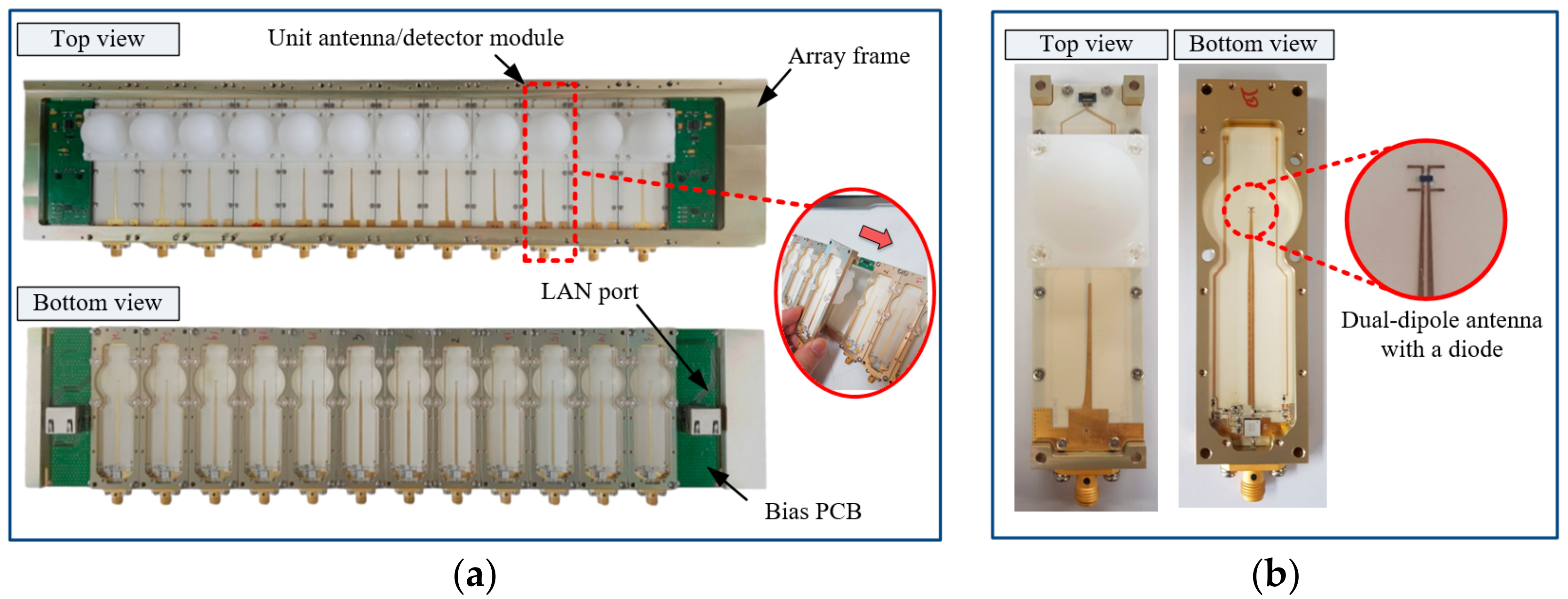
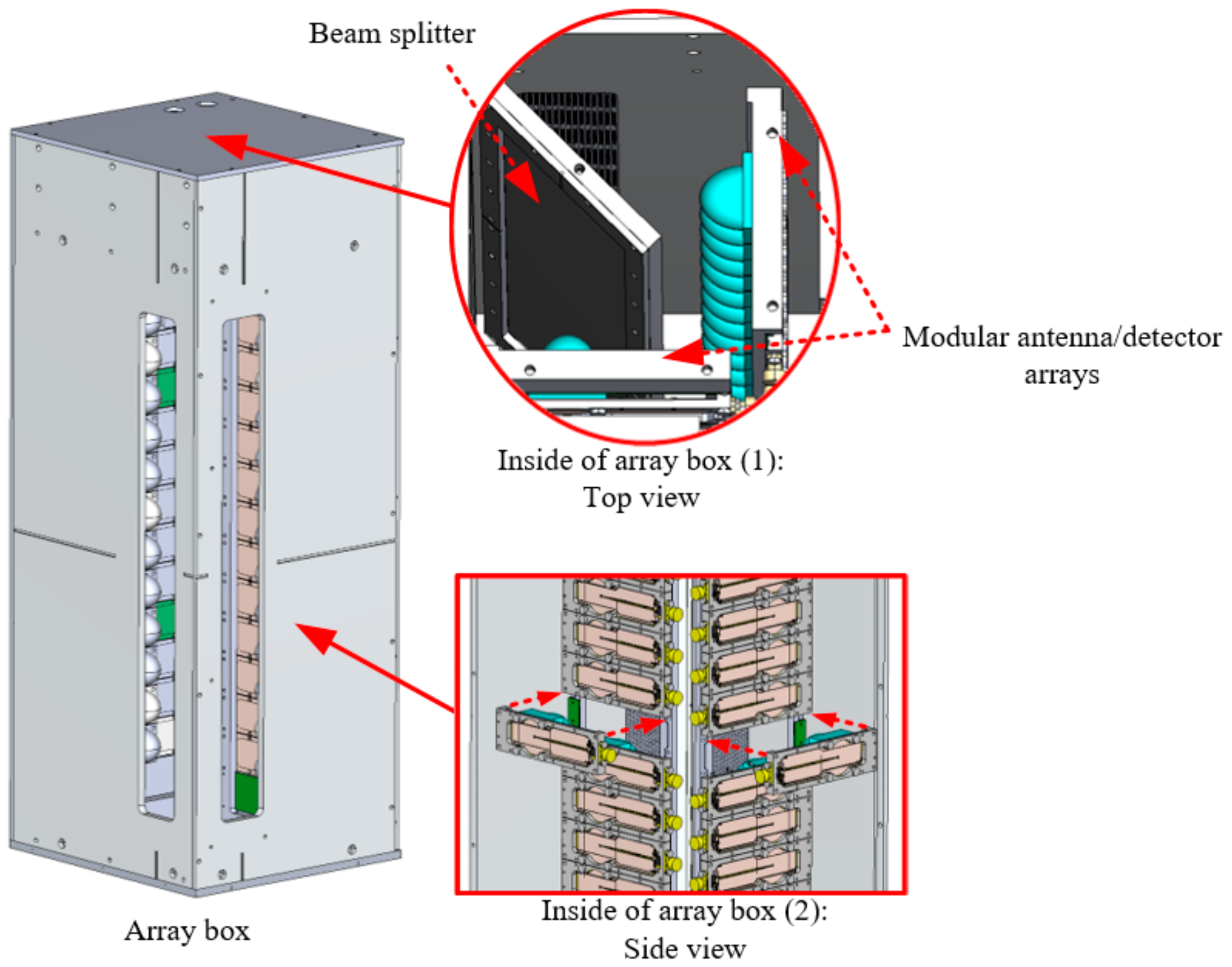
3.1. Modular Antenna/Detector Array
3.2. Unit Antenna/Detector Module
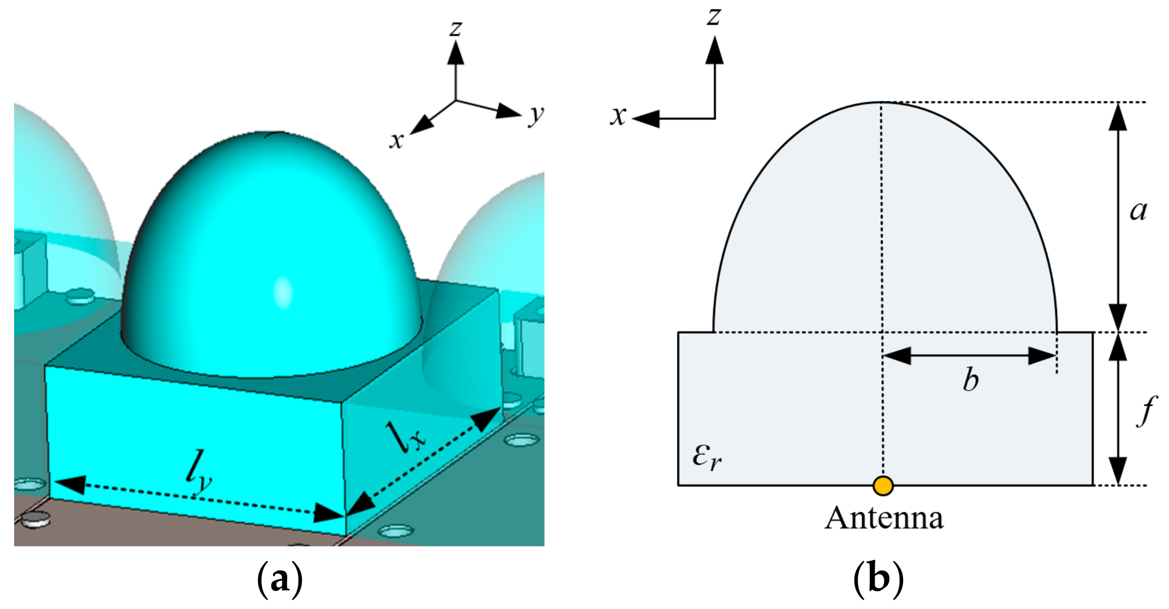
3.2.1. Elliptical Mini-Lens
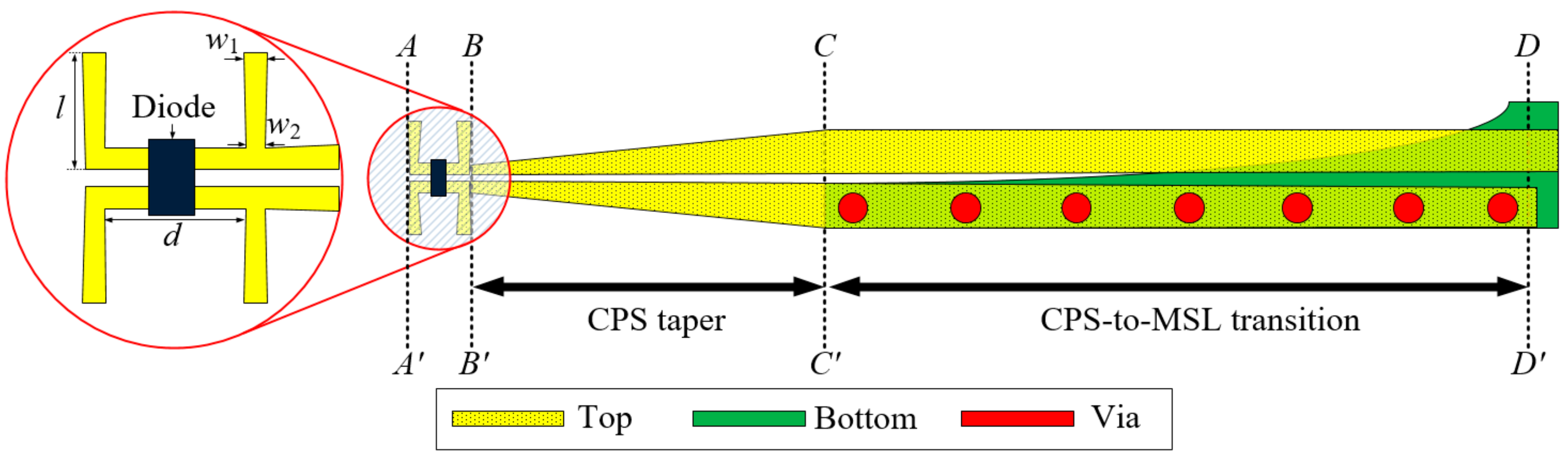
3.2.2. Dual-Dipole Antenna/Detector with an Ultra-Wideband Antenna Balun
4. Fabrication and Measurement
4.1. Fabrication
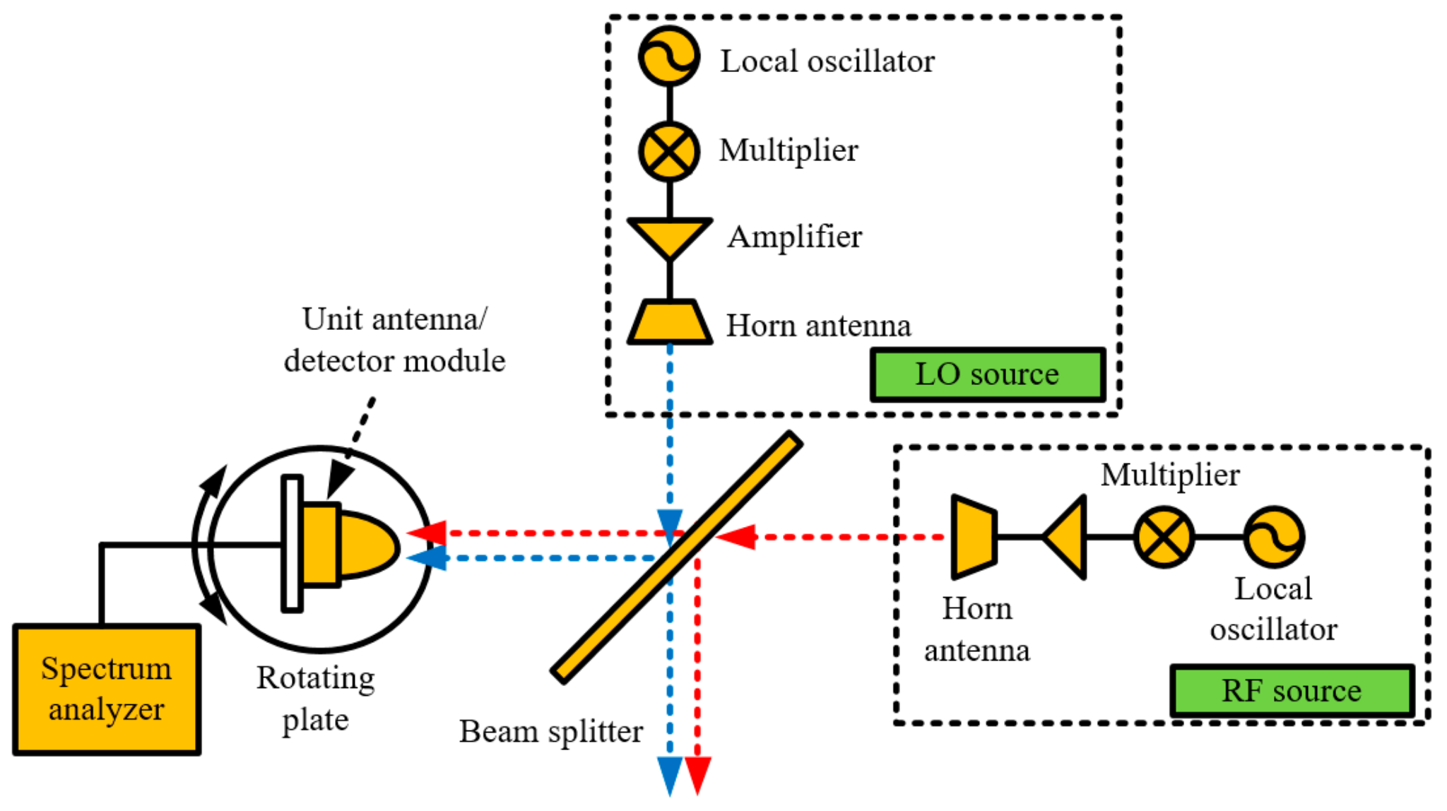
4.2. Measurements
4.3. Proposed Modular Antenna/Detector Array for KSTAR Operation
5. Conclusions
Author Contributions
Funding
Institutional Review Board Statement
Informed Consent Statement
Data Availability Statement
Conflicts of Interest
References
- Wesson, J.; Campbell, D.J. Tokamaks, 2nd ed.; Oxford Science Publications: New York, NY, USA, 2004; pp. 2–7. [Google Scholar]
- Yun, G.S.; Lee, W.; Choi, M.J.; Lee, J.; Park, H.K.; Tobias, B.; Domier, C.W.; Luhmann, N.C., Jr.; Donné, A.J.H.; Lee, J.H.; et al. Two-Dimensional Visualization of Growth and Burst of the Edge-Localized Filaments in KSTAR H-Mode Plasmas. Phys. Rev. Lett. 2011, 107, 045004. [Google Scholar] [CrossRef] [PubMed] [Green Version]
- Park, H.K.; Luhmann, N.C., Jr.; Donné, A.J.H.; Classen, I.G.J.; Domier, C.W.; Mazzucato, E.; Munsat, T.; van de Pol, M.J.; Xia, Z.; TEXTOR Team. Observation of High-Field-Side Crash and Heat Transfer during Sawtooth Oscillation in Magnetically Confined Plasmas. Phys. Rev. Lett. 2006, 96, 195003. [Google Scholar] [CrossRef] [PubMed] [Green Version]
- Yun, G.S.; Park, H.K.; Lee, W.; Choi, M.J.; Choe, G.H.; Park, S.; Bae, Y.S.; Lee, K.D.; Yoon, S.W.; Jeon, Y.M.; et al. Appearance and Dynamics of Helical Flux Tubes under Electron Cyclotron Resonance Heating in the Core of KSTAR Plasmas. Phys. Rev. Lett. 2012, 109, 145003. [Google Scholar] [CrossRef] [PubMed] [Green Version]
- Classen, I.G.J.; Westerhof, E.; Domier, C.W.; Donné, A.J.H.; Jaspers, R.J.E.; Luhmann, N.C., Jr.; Park, H.K.; van de Pol, M.J.; Spakman, G.W.; Jakubowski, M.W.; et al. Effect of Heating on the Suppression of Tearing Modes in Tokamaks. Phys. Rev. Lett. 2007, 98, 035001. [Google Scholar] [CrossRef] [PubMed] [Green Version]
- Munsat, T.; Domier, C.W.; Kong, X.; Liang, T.; Luhmann, N.C., Jr.; Tobias, B.; Lee, W.; Park, H.K.; Yun, G.S.; Classen, I.G.J.; et al. Electron cyclotron emission imaging in tokamak plasmas. Appl. Opt. 2010, 49, E20–E30. [Google Scholar] [CrossRef] [PubMed]
- Zhu, Y.L.; Xie, J.L.; Yu, C.X.; Zhao, Z.L.; Gao, B.X.; Chen, D.X.; Liu, W.D.; Liao, W.; Qu, C.M.; Luo, C.; et al. Millimeter-wave imaging diagnostics systems on the EAST tokamak. Rev. Sci. Instrum. 2016, 87, 11D901. [Google Scholar] [CrossRef] [PubMed]
- Wang, J.; Domier, C.W.; Xia, Z.G.; Liang, Y.; Luhmann, N.C., Jr.; Park, H.; Munsat, T.; Mazzucato, E.; van de Pol, M.J.; Classen, I.G.J.; et al. Two-dimensional electron cyclotron emission imaging diagnostic for TEXTOR. Rev. Sci. Instrum. 2004, 75, 3875–3877. [Google Scholar] [CrossRef]
- Deng, B.H.; Domier, C.W.; Luhmann, N.C.; Donné, A.J.H.; van de Pol, M.J. Electron cyclotron emission imaging diagnostic on TEXTOR. Rev. Sci. Instrum. 2001, 72, 368–370. [Google Scholar] [CrossRef] [Green Version]
- Rowan, W.; Austin, M.; Beno, J.; Ellis, R.; Feder, R.; Ouroua, A.; Patel, A.; Phillips, P. Electron cyclotron emission diagnostic for ITER. Rev. Sci. Instrum. 2010, 81, 10D935. [Google Scholar] [CrossRef]
- Yun, G.S.; Lee, W.; Choi, M.J.; Kim, J.B.; Park, H.K.; Domier, C.W.; Tobias, B.; Liang, T.; Kong, X.; Luhmann, N.C., Jr.; et al. Development of KSTAR ECE imaging system for measurement of temperature fluctuations and edge density fluctuations. Rev. Sci. Instrum. 2010, 81, 10D930. [Google Scholar] [CrossRef]
- Janicki, C. Electron temperature measurement from the ECE diagnostics in tokamak plasmas under transient conditions. Nucl. Fusion 1993, 33, 513–516. [Google Scholar] [CrossRef]
- Piliya, A.D.; Popov, A.Y. Theory of ECE fluctuations in tokamak plasmas. Plasma Phys. Control. Fusion 2002, 44, 2051–2062. [Google Scholar] [CrossRef]
- Yun, G.S.; Lee, W.; Choi, M.J.; Lee, J.; Kim, M.; Leem, J.; Nam, Y.; Choe, G.H.; Park, H.K.; Park, H.; et al. Quasi 3D ECE imaging system for study of MHD instabilities in KSTAR. Rev. Sci. Instrum. 2014, 85, 11D820. [Google Scholar] [CrossRef] [Green Version]
- Yang, H.L.; Park, Y.M.; Bae, Y.S.; Kim, H.K.; Kim, K.M.; Lee, K.S.; Bang, E.N.; Kim, H.T.; Lee, H.J.; Kwag, S.W.; et al. Development of KSTAR in-vessel components and heating systems. Fusion Eng. Des. 2011, 86, 588–592. [Google Scholar] [CrossRef]
- Lee, W.; Yun, G.S.; Park, H.K.; Nam, Y.B.; Seon, C.R. The conceptual design of an electron cyclotron emission imaging system for studying ITER-like high temperature plasmas. Plasma Phys. Control. Fusion 2014, 56, 95017. [Google Scholar] [CrossRef]
- Pan, X.M.; Yang, Z.J.; Ma, X.D.; Zhu, Y.L.; Luhmann, N.C., Jr.; Domier, C.W.; Ruan, B.W.; Zhuang, G. Design of the 2D electron cyclotron emission imaging instrument for the J-TEXT tokamak. Rev. Sci. Instrum. 2016, 87, 11E106. [Google Scholar] [CrossRef] [PubMed]
- Nam, Y.B.; Park, H.K.; Lee, W.; Yun, G.S.; Kim, M.; Sabot, R.; Elbeze, D.; Lotte, P.; Shen, J. Compact ECEI system with in-vessel reflective optics for WEST. Rev. Sci. Instrum. 2016, 87, 11E135. [Google Scholar] [CrossRef] [PubMed]
- Zhu, Y.; Yu, J.H.; Yu, G.; Ye, Y.; Tobias, B.; Diallo, A.; Kramer, G.; Ren, Y.; Domier, C.W.; Li, X.; et al. W-band system-on-chip electron cyclotron emission imaging system on DIII-D. Rev. Sci. Instrum. 2020, 91, 093504. [Google Scholar] [CrossRef]
- Lee, G.H.; Kumar, S.; Choi, H.C.; Kim, K.W. Wideband High-Gain Double-Sided Dielectric Lens Integrated with a Dual-Bowtie Antenna. IEEE Antennas Wirel. Propag. Lett. 2021, 20, 293–297. [Google Scholar] [CrossRef]
- Zhang, P.; Domier, C.W.; Liang, T.; Kong, X.; Tobias, B.; Shen, Z.; Luhmann, N.C., Jr.; Park, H.; Classen, I.G.J.; van de Pol, M.J.; et al. The next generation of electron cyclotron emission imaging diagnostics. Rev. Sci. Instrum. 2008, 79, 10F103. [Google Scholar] [CrossRef] [Green Version]
- Filipovic, D.F.; Gearhart, S.S.; Rebeiz, G.M. Double-Slot Antennas on Extended Hemispherical and Elliptical Silicon Dielectric Lenses. IEEE Trans. Microw. Theory Tech. 1993, 41, 1738–1749. [Google Scholar] [CrossRef]
- Lai, J.; Domier, C.; Luhmann, N.C., Jr. Slot Dual Dipole Antenna with Miniature Elliptical Substrate Lenses for Millimeter-Wave Imaging. Eur. Microw. Conf. 2013, 7, 1751–1754. [Google Scholar]
- Lee, G.H.; Mohyuddin, W.; Choi, H.C.; Kim, K.W. Asymmetric Ultra-Wideband Microstrip-to-Coplanar Stripline Transition. IEEE Microw. Wirel. Compon. Lett. 2018, 28, 386–388. [Google Scholar] [CrossRef]
- Lee, G.H.; Kumar, S.; Mohyuddin, W.; Choi, H.C.; Kim, K.W. Generalized Design Technique of Ultra-Wideband Transitions for Quasi-TEM Planar Transmission Lines Based on Analytical Models. IEEE Access 2021, 9, 52619–52633. [Google Scholar] [CrossRef]
- Lee, G.H.; Mohyuddin, W.; Kumar, S.; Choi, H.C.; Kim, K.W. Compact Wideband Coplanar Stripline-to-Microstrip Line Transition Using a Bended Structure on a Two-Layered Substrate. Electronics 2021, 10, 1272. [Google Scholar] [CrossRef]


Publisher’s Note: MDPI stays neutral with regard to jurisdictional claims in published maps and institutional affiliations. |
© 2022 by the authors. Licensee MDPI, Basel, Switzerland. This article is an open access article distributed under the terms and conditions of the Creative Commons Attribution (CC BY) license (https://creativecommons.org/licenses/by/4.0/).
Share and Cite
Lee, G.H.; Lee, J.S.; Kim, D.H.; Nashuha, S.H.; Kim, M.J.; Min, B.C.; Lee, J.H.; Lee, W.C.; Yun, G.S.; Kim, T.G.; et al. W-Band Modular Antenna/Detector Array for the Electron Cyclotron Emission Imaging System in KSTAR. Appl. Sci. 2022, 12, 2431. https://doi.org/10.3390/app12052431
Lee GH, Lee JS, Kim DH, Nashuha SH, Kim MJ, Min BC, Lee JH, Lee WC, Yun GS, Kim TG, et al. W-Band Modular Antenna/Detector Array for the Electron Cyclotron Emission Imaging System in KSTAR. Applied Sciences. 2022; 12(5):2431. https://doi.org/10.3390/app12052431
Chicago/Turabian StyleLee, Gwan Hui, Jung Seok Lee, Dong Hwi Kim, Syifa Haunan Nashuha, Mun Ju Kim, Byung Cheol Min, Jae Hyun Lee, Woo Chang Lee, Gun Su Yun, Tae Gyu Kim, and et al. 2022. "W-Band Modular Antenna/Detector Array for the Electron Cyclotron Emission Imaging System in KSTAR" Applied Sciences 12, no. 5: 2431. https://doi.org/10.3390/app12052431