
A Potentiostat Readout Circuit with a Low-Noise and Mismatch-Tolerant Current Mirror Using Chopper Stabilization and Dynamic Element Matching for Electrochemical Sensors


Abstract
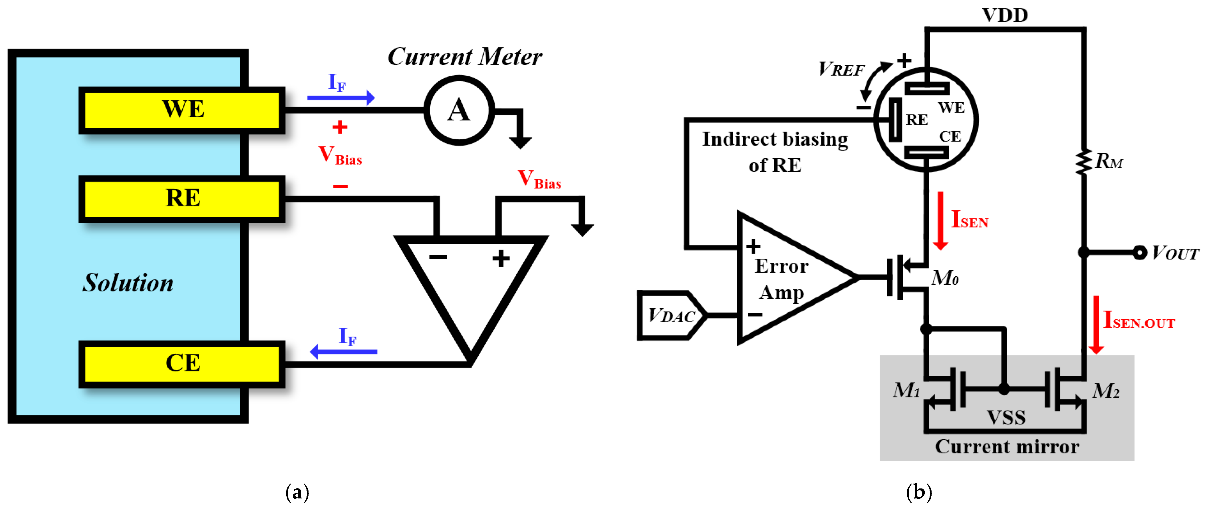
:1. Introduction
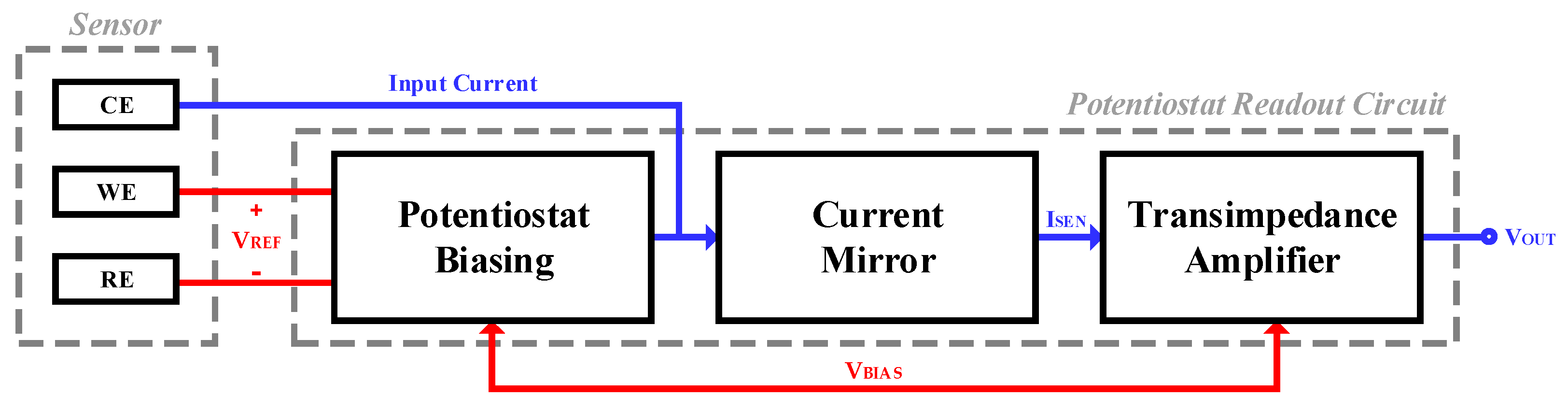
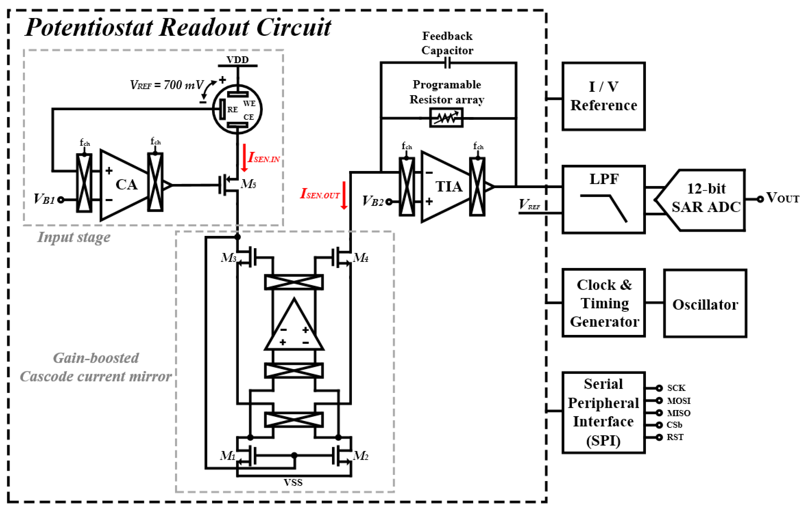
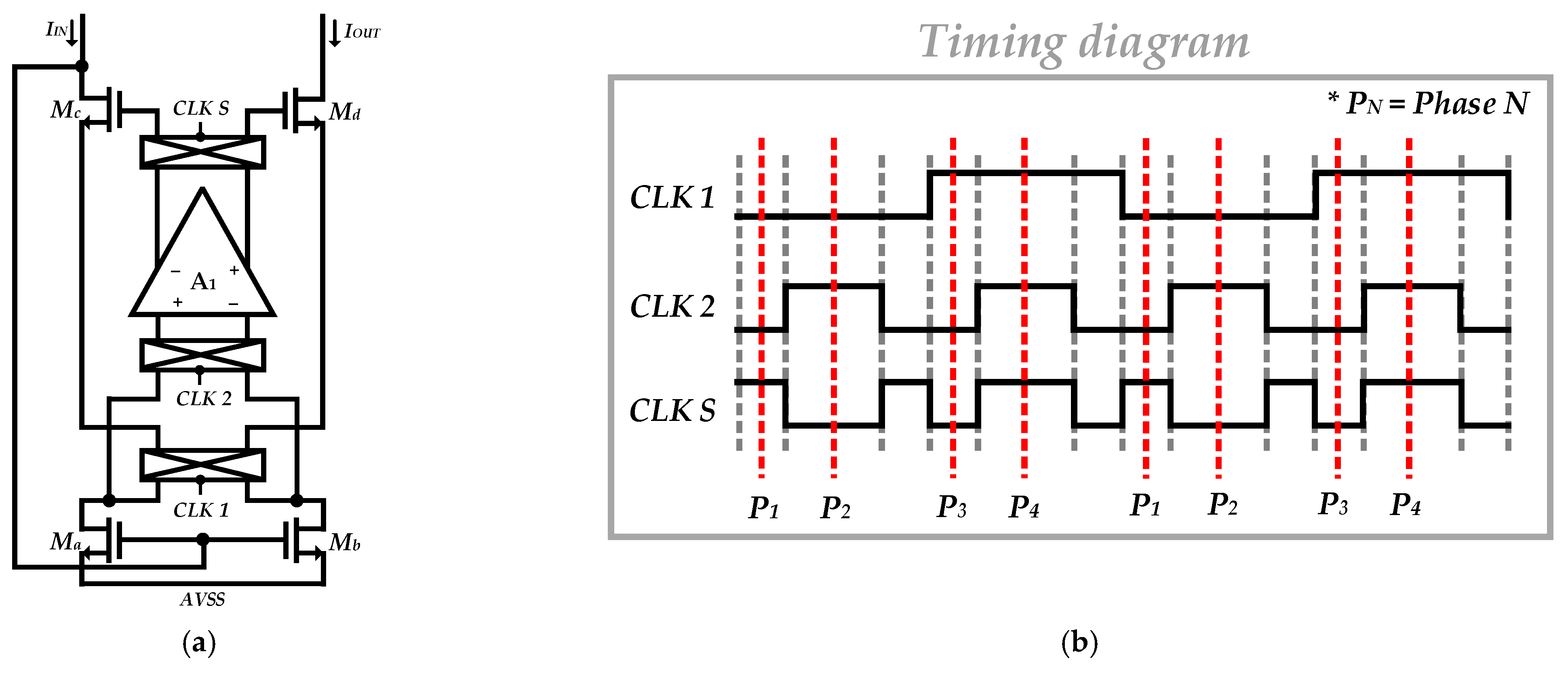
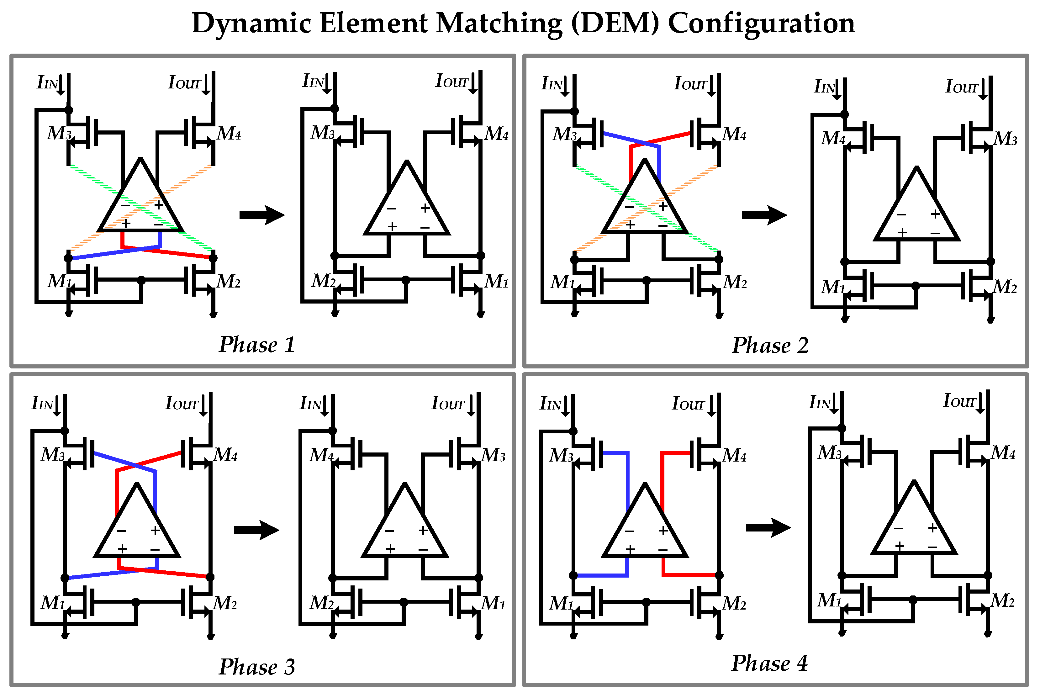
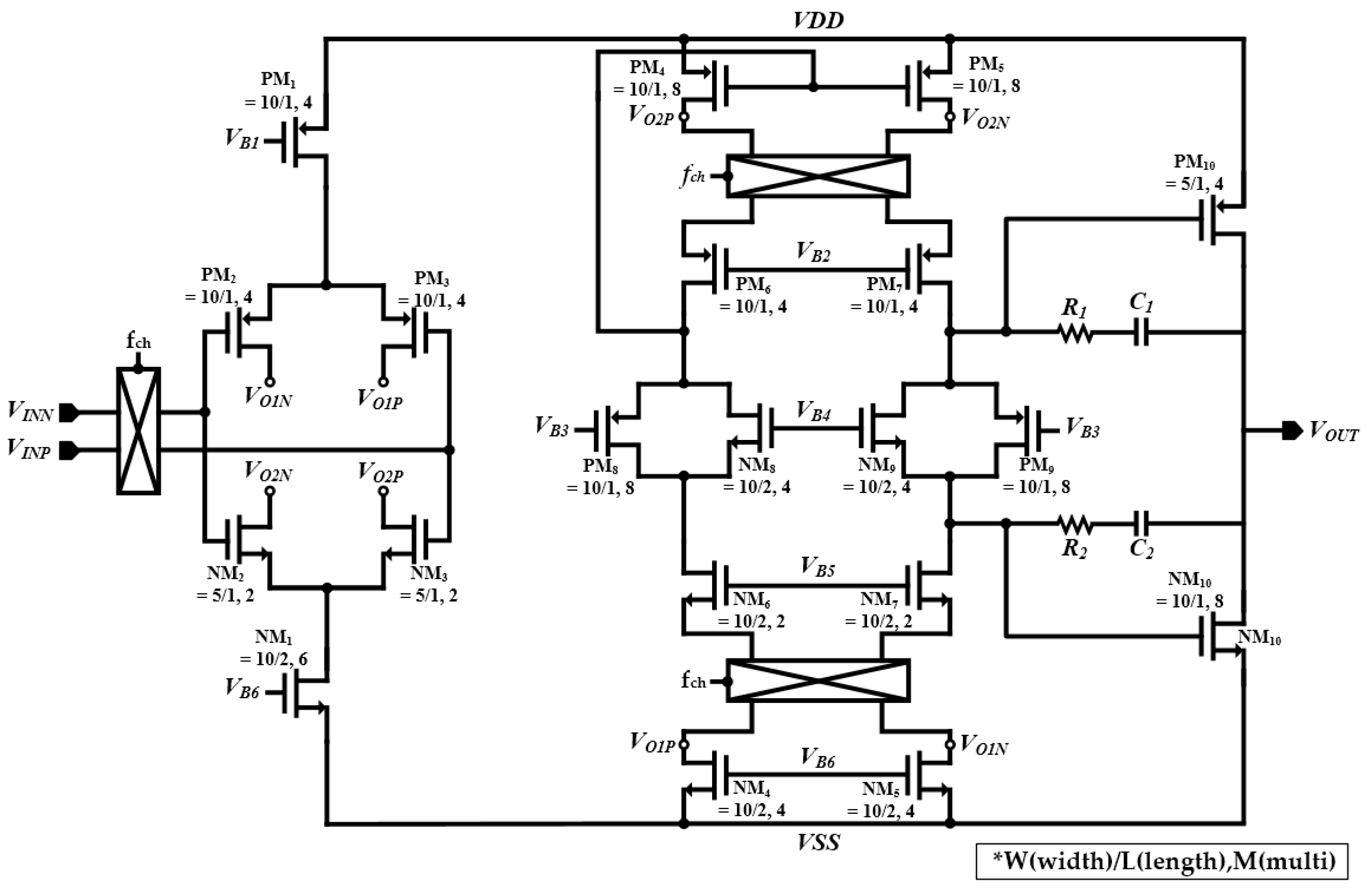
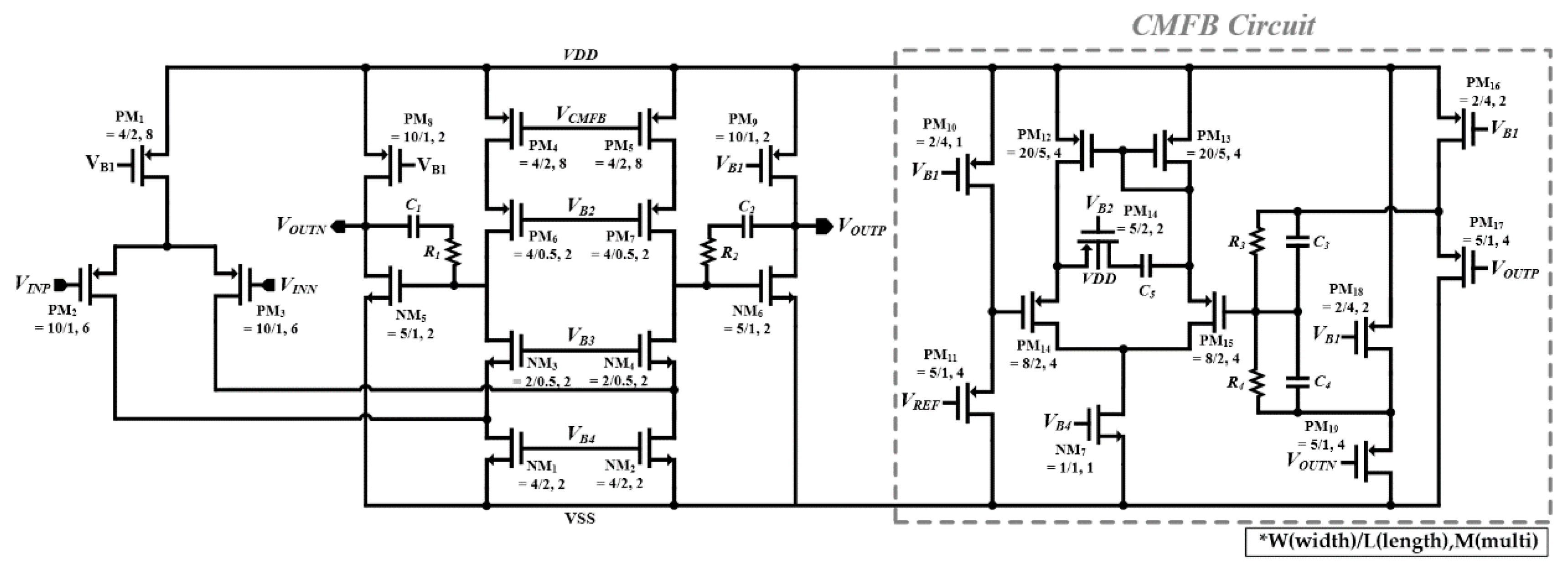
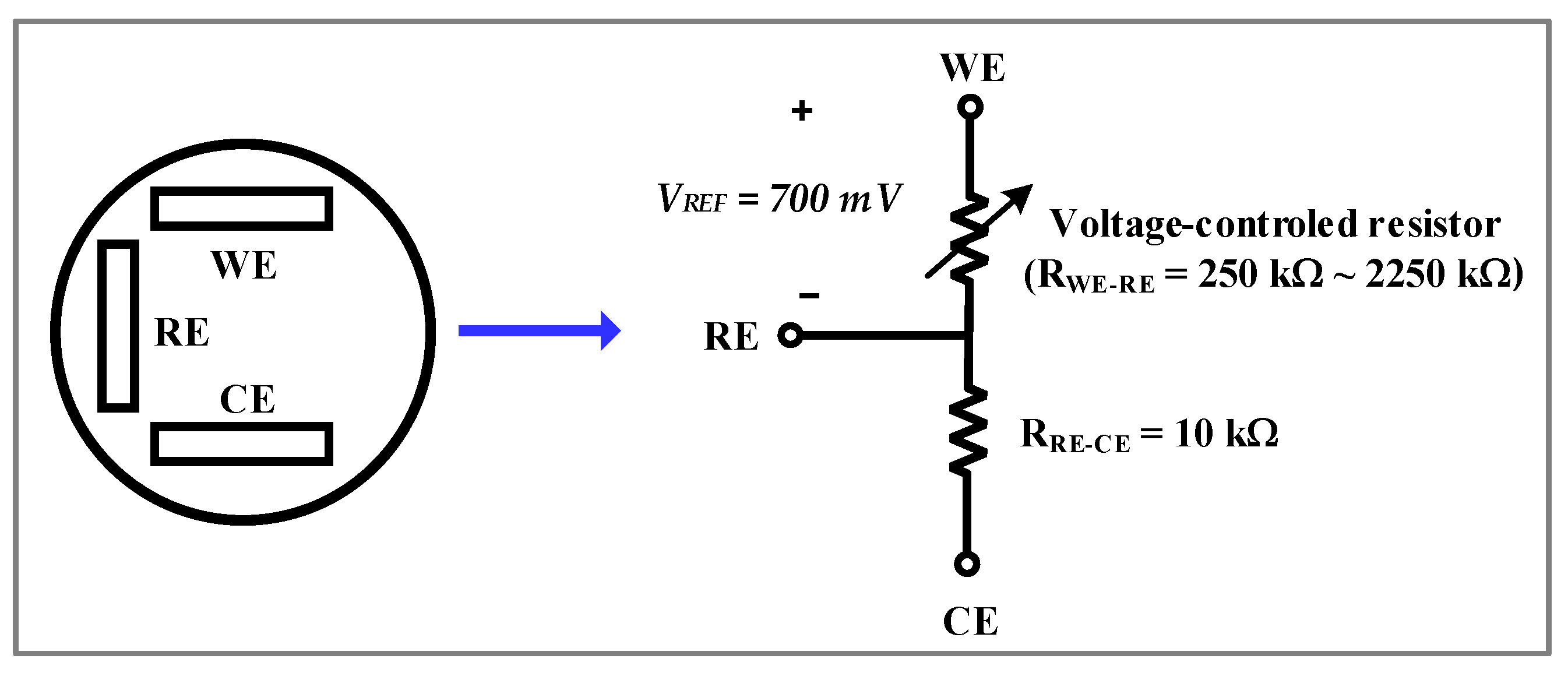
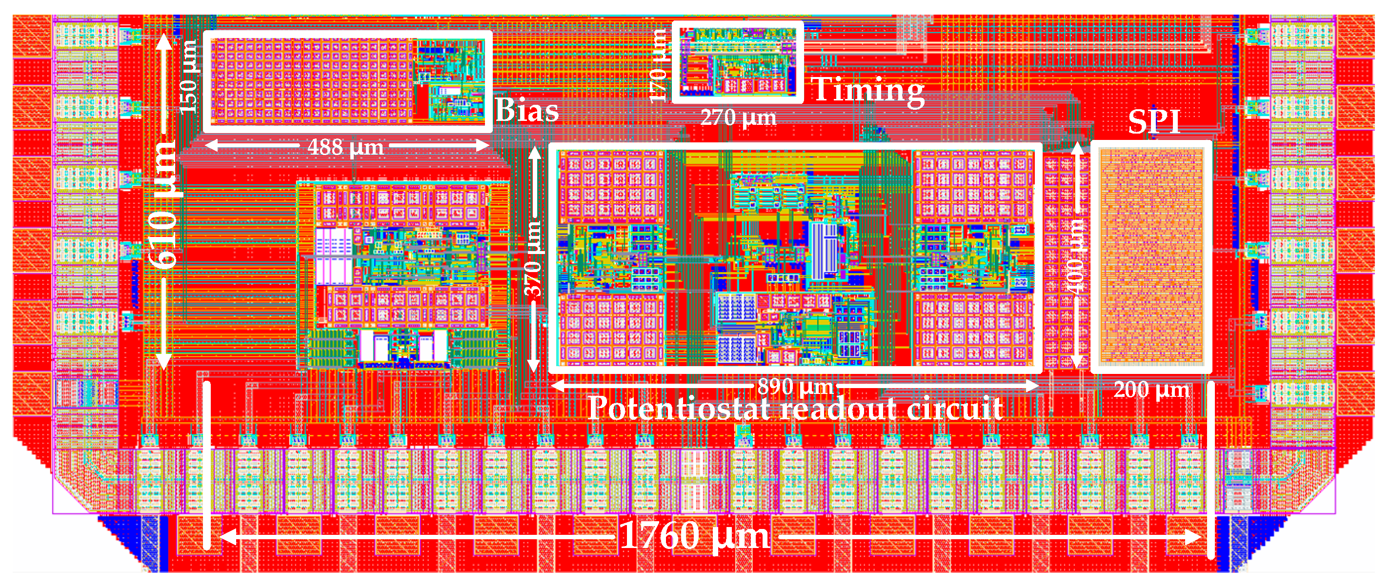
2. Proposed Current-Mirror-Based Potentiostat Readout Circuit
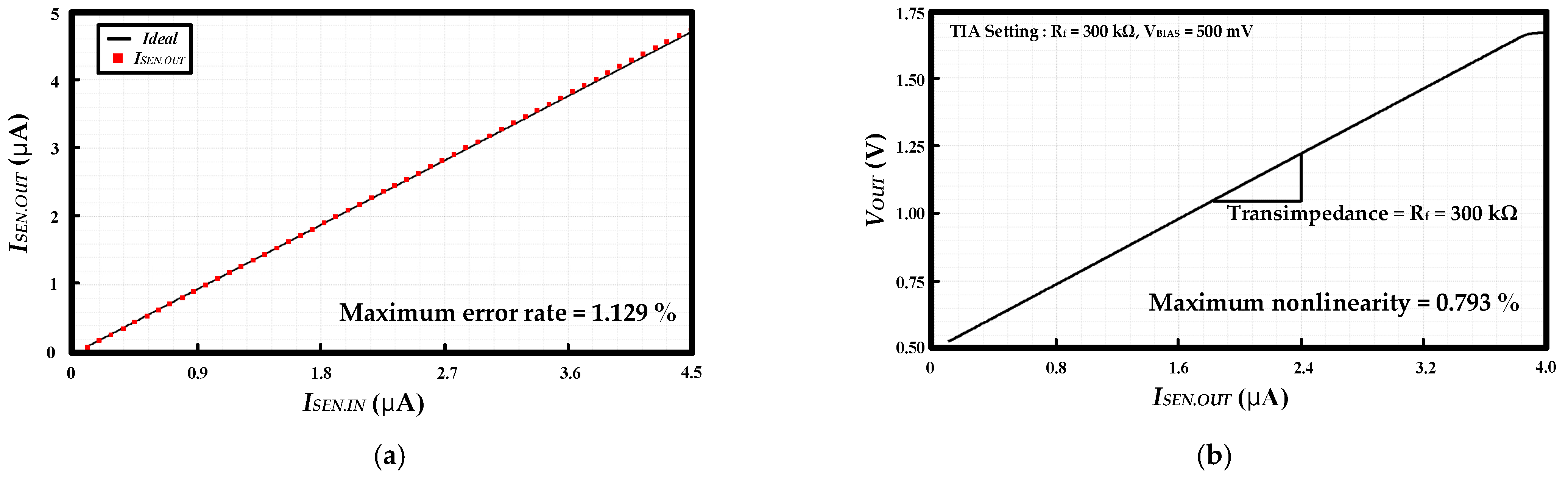
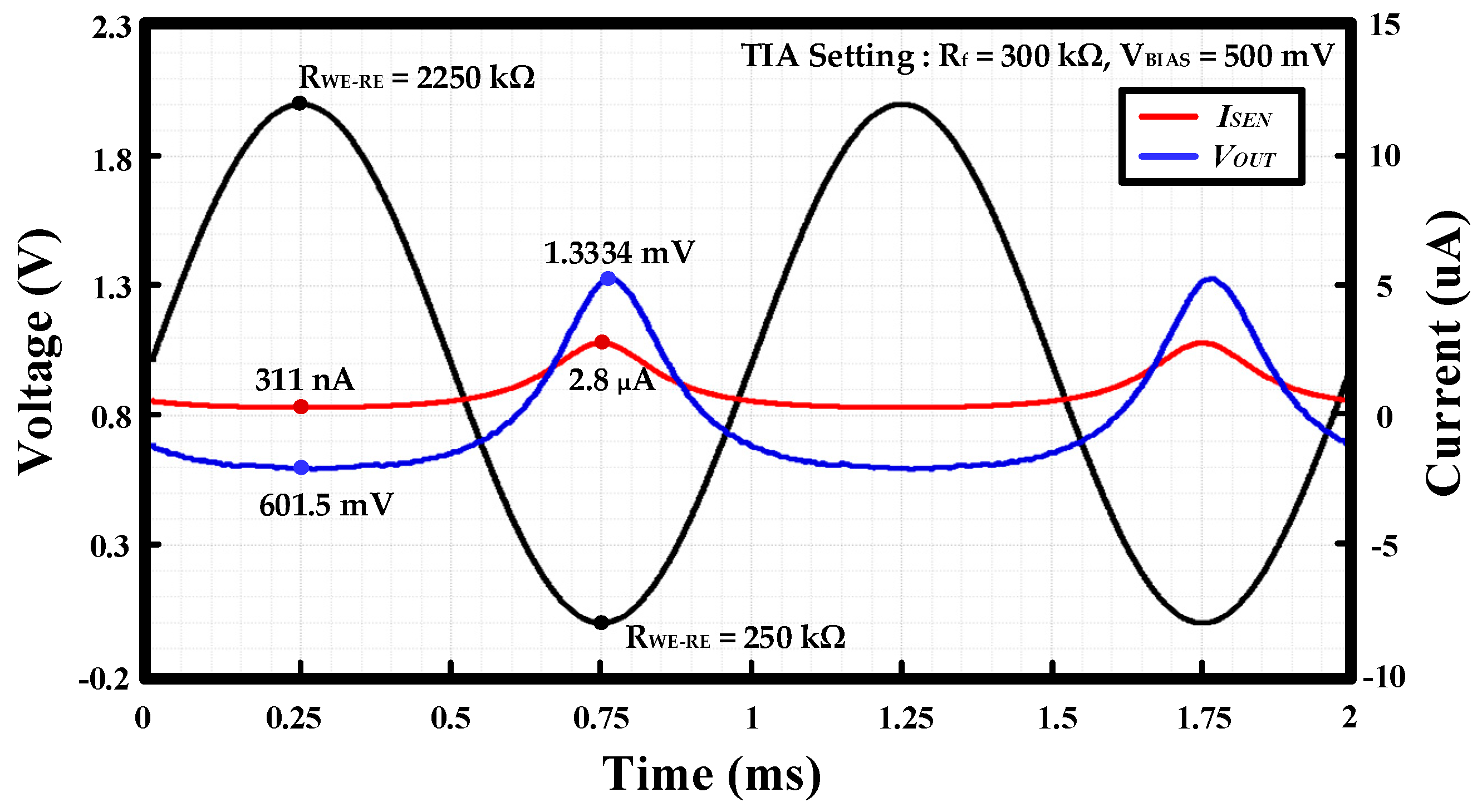
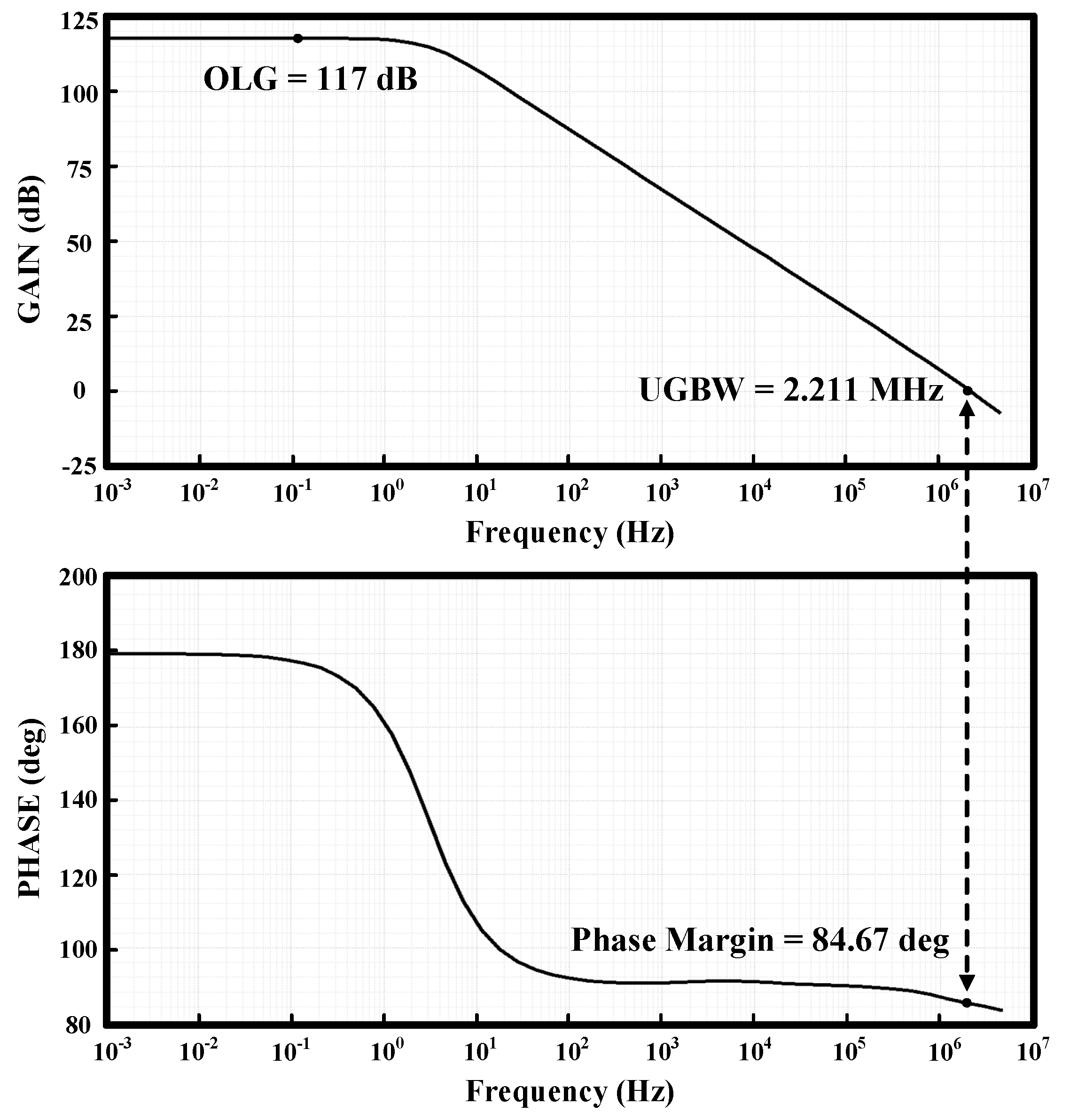
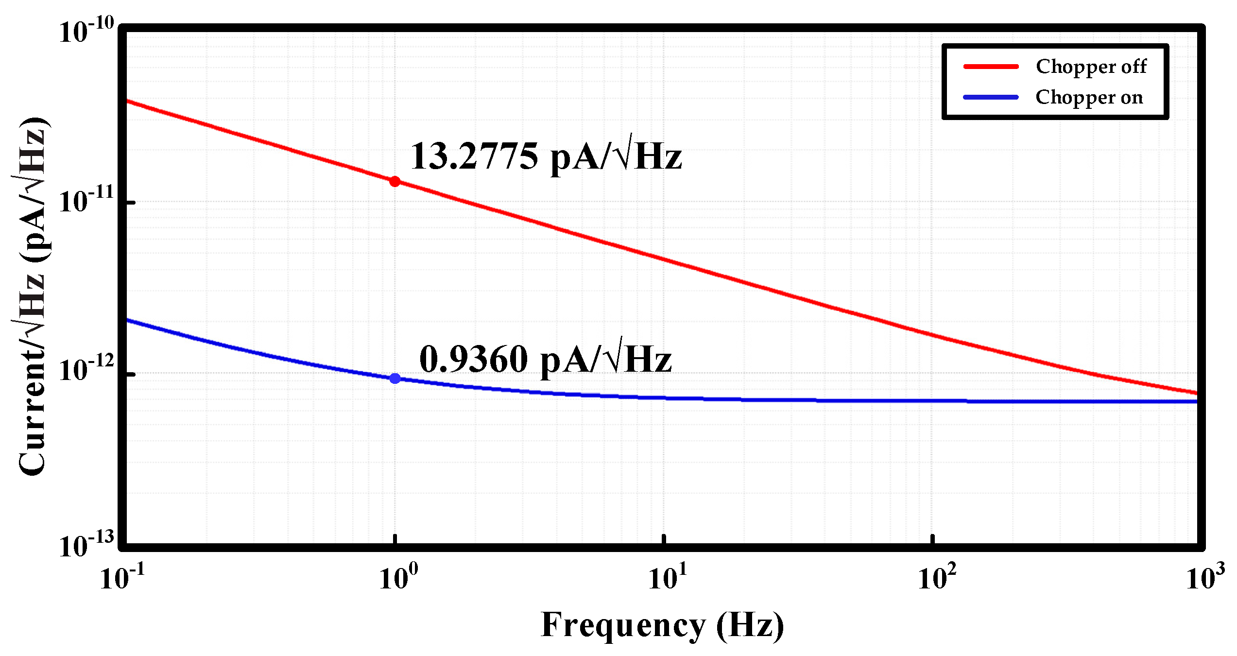
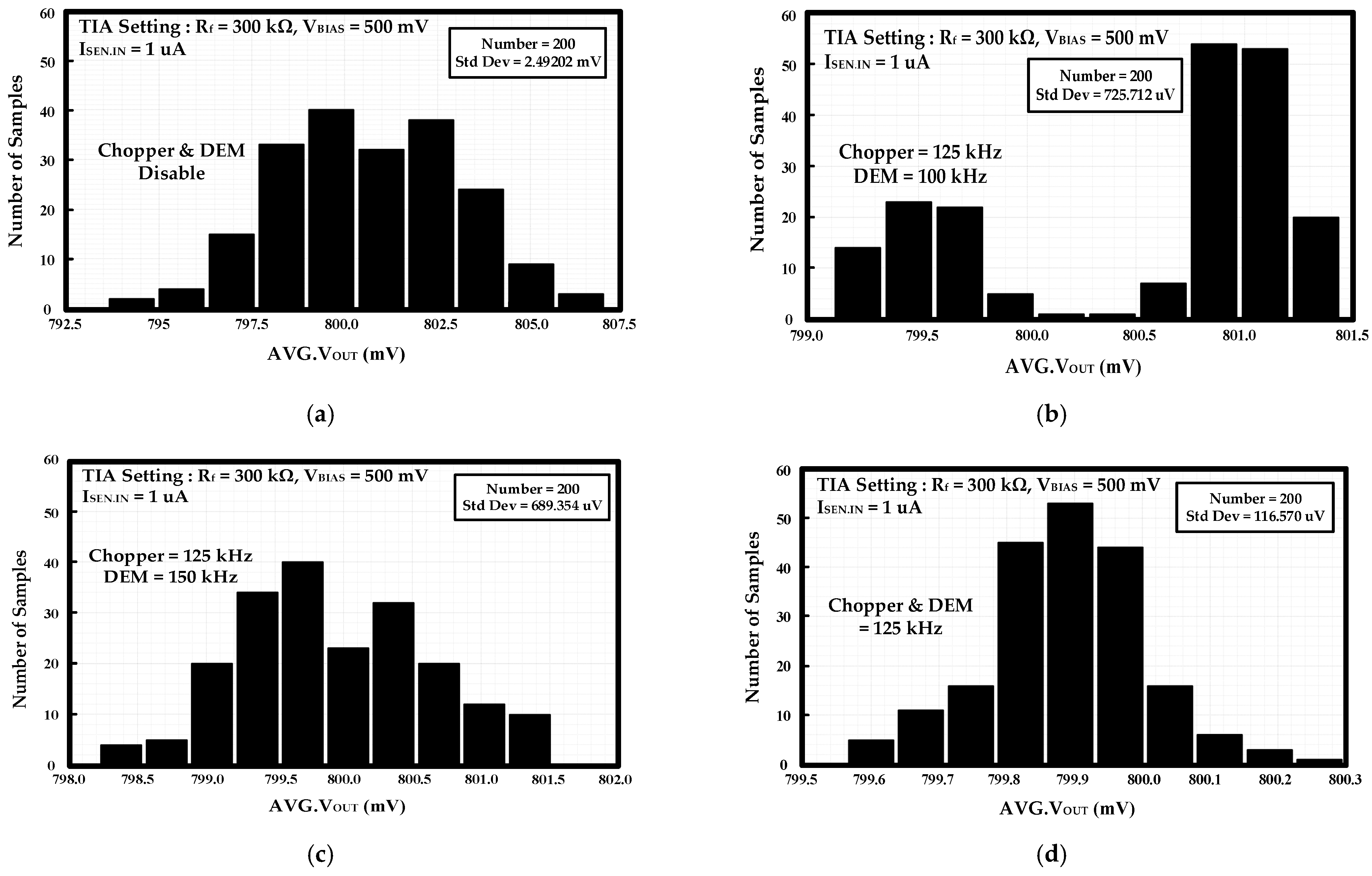
3. Results and Discussions
4. Conclusions
Author Contributions
Funding
Institutional Review Board Statement
Informed Consent Statement
Data Availability Statement
Acknowledgments
Conflicts of Interest
References
- Kim, J.; Ko, H. A 1.2 V low-power CMOS chopper-stabilized analog front-end IC for glucose monitoring. IEEE Sens. J. 2015, 16, 6517–6518. [Google Scholar] [CrossRef]
- Zuo, L.; Islam, S.K.; Mahbub, I.; Quaiyum, F. A low-power 1-V potentiostat for glucose sensors. IEEE Trans. Circuits Syst. II Express Briefs 2015, 62, 204–208. [Google Scholar] [CrossRef]
- Kwon, J.; Lee, Y.; Lee, T.; Ahn, J. Aptamer-based field-effect transistor for detection of avian influenza virus in chicken serum. Anal. Chem. 2020, 92, 5524–5531. [Google Scholar] [CrossRef] [PubMed]
- Ahmadi, M.M.; Jjulien, G.A. Current-mirror-based potentiostats for three-electrode amperometric electrochemical sensors. IEEE Trans. Circuits Syst. I Regul. Pap. 2009, 56, 1339–1348. [Google Scholar] [CrossRef]
- Chung, W.; Paglinawan, A.C.; Kuo, T. A 600 μW readout circuit with potentiostat for amperometric chemical sensors and glucose meter applications. In Proceedings of the 2007 IEEE Conference on Electron Devices and Solid-State Circuits, Tainan, Taiwan, 20–22 December 2007. [Google Scholar] [CrossRef]
- Ahmadi, M.M.; Jullien, G.A. A very low power CMOS potentiostat for bioimplantable applications. In Proceedings of the Fifth International Workshop on System-on-Chip for Real-Time Application (IWSOC’05), Banff, AB, Canada, 20–24 July 2005; pp. 184–189. [Google Scholar] [CrossRef]
- Bouhoun, M.L.; Blondeau, P.; Louafi, Y.; Andrade, F.J. A Paper-Based Potentiometric Platform for Determination of Water Hardness. Chemosensors 2021, 9, 96. [Google Scholar] [CrossRef]
- Wang, W.-S.; Kuo, W.-T.; Huang, H.-Y.; Luo, C.-H. Wide dynamic range CMOS potentiostat for amperometric chemical sensor. Sensors 2010, 10, 1782–1797. [Google Scholar] [CrossRef] [PubMed]
- Matzeu, G.; Florea, L.; Diamond, D. Advances in wearable chemical sensor design for monitoring biological fluids. Sens. Actuators B Chem. 2015, 211, 403–418. [Google Scholar] [CrossRef]
- Lefrou, C.; Fabry, P.; Poignet, J.C. Electrochemistry; Springer: Berlin, Germany, 2009; pp. 68–90. [Google Scholar]
- Mohanty, S.P.; Konugianos, E. Biosensors: A tutorial review. IEEE Potentials 2006, 25, 35–40. [Google Scholar] [CrossRef]
- Fischer, S.; Muratore, D.; Weinreich, S.; Peres, A.P.; Walker, R.M.; Gupta, C.; Howe, R.T.; Murmann, B. Low-noise integrated potentiostat for affinity-free protein detection with 12 nV/rt-Hz at 30 Hz and 1.8 pArms Resolution. IEEE Solid-State Circuits Lett. 2019, 6, 41–44. [Google Scholar] [CrossRef]
- Martin, S.M.; Gebara, F.H.; Strong, T.D.; Brown, R.B. A fully differential potentiostat. IEEE Sens. J. 2009, 9, 135–142. [Google Scholar] [CrossRef]
- Ayers, S.; Gillis, K.D.; Lindau, M.; Minch, B.A. Design of a CMOS potentiostat circuit for electrochemical detector arrays. IEEE Trans. Circuits Syst. I Regul. Pap. 2007, 54, 736–744. [Google Scholar] [CrossRef] [PubMed] [Green Version]
- Turner, R.F.B.; Harrison, D.J.; Baltes, H.P. A CMOS potentiostat for amperometric chemical sensors. IEEE J. Solid-State Circuits 1987, 22, 473–478. [Google Scholar] [CrossRef]
- Jafari, H.M.; Genov, R. Bidirectional current conveyer with chopper stabilization and dynamic element matching. In Proceedings of the 2021 IEEE International Symposium on Circuits and Systems (ISCAS), Seoul, Korea, 20–23 May 2012; pp. 1079–1082. [Google Scholar] [CrossRef]
- Jafari, H.M.; Genov, R. Chopper-stabilized bidirectional current acquisition circuits for electrochemical amperometric biosensors. IEEE Trans. Circuits Syst. I: Regul. Pap. 2013, 60, 1149–1157. [Google Scholar] [CrossRef]
- Rooijers, T.; Karmakar, S.; Kusuda, Y.; Huijsing, J.H.; Makinwa, K.A.A. 31.4 A Chopper-Stabilized Amplifier with-107dB IMD and 28 dB Suppression of Chopper-Induced IMD. In Proceedings of the 2021 IEEE International Solid-State Circuits Conference (ISSCC), San Fransisco, CA, USA, 13–22 February 2021; pp. 440–480. [Google Scholar] [CrossRef]
- Busoni, L.; Carla, M.; Lanzi, L. A comparison between potentiostatic circuits with grounded work or auxiliary electrode. Rev. Sci. Instrum. 2002, 73, 1921. [Google Scholar] [CrossRef]
- Fidler, J.C.; Penrose, W.R.; Bovis, J.P. A potentiostat based on a voltage-controlled current source for use with amperometric gas sensors. IEEE Trans. Instrum. Meas. 1992, 41, 308–310. [Google Scholar] [CrossRef]
- Anoop, A.E.; Mohan, N.M.; Guruvayurappan, K. Simulation of a multi-strip blood glucometer. In Proceedings of the TENCON 2014—2014 IEEE Rehion 10 Conference, Bankok, Thailand, 22–25 October 2014; pp. 1–4. [Google Scholar] [CrossRef]
- Nazari, M.H.; Mazhab-Jafari, H.; Leng, L.; Guenther, A.; Genov, R. CMOS neurotransmitter microarray: 96-channel integrated potentiostat with on-die microsensors. IEEE Trans. Biomed. Circuits Syst. 2013, 7, 338–348. [Google Scholar] [CrossRef] [PubMed]
- Ghodsevali, E.; Morneau-Gamache, S.; Mathault, J.; Landari, H.; Boisselier, É.; Boukadoum, M.; Gosselin, B.; Miled, A. Miniaturized FDDA and CMOS based potentiostat for bio-applications. Sensors 2017, 17, 810. [Google Scholar] [CrossRef] [PubMed] [Green Version]
- Aymerich, J.; Marquez, A.; Munoz-Berbel, X.; Javier Del Campo, F.; Guirado, G.; Teres, L.; Serra-Graells, F.; Dei, M. A 15-μW 105-dB 1.8-Vpp potentiostatic delta-sigma modulator for wearable electrochemical transducers in 65-nm CMOS technology. IEEE Access 2020, 8, 62127–62136. [Google Scholar] [CrossRef]


| Transistor | Noise Source | Total Noise Chopper Disable (%) | Total Noise Chopper Enable (%) |
|---|---|---|---|
| M1,2 (current mirror) | Flicker | 71.52 | 12.44 |
| M1,2 (current mirror) | Thermal | 8.03 | 31.02 |
| PM2,3 (TIA input pair) | Flicker | 4.06 | 1.40 |
| NM2,3 (TIA input pair) | Flicker | 3.62 | 1.38 |
| PM4,5 (TIA cascode load) | Flicker | 3.53 | 0.18 |
| NM4,5 (TIA cascode load) | Flicker | 2.8 | 0.10 |
| NM6,7 (TIA cascode) | Flicker | 0.18 | 2.78 |
| This Work (Simulated) | TBCAS 2013 [22] | TCAS-I 2009 [4] | Sensors 2017 [23] | IEEE Access 2020 [24] | ISCAS 2012 [16] TCAS-I 2013 [17] | |
|---|---|---|---|---|---|---|
| Process(μm) | 0.18 | 0.35 | 0.18 | 0.18 | 0.065 | 0.13 |
| Architecture | Current mirror | CC 1 | Current mirror | FDDA 2 | 1st-order delta-sigma converter | CC |
| Chopper | Y (125 kHz) | N | N | N | N | Y (10 kHz) |
| DEM O/X | Y (125 kHz) | N | N | N | N | Y (500 Hz) |
| Output format | Voltage | Digital codes | Frequency | Voltage | Digital codes | Current |
| Supply voltage (V) | 1.8 | 3.3 | 1.8 | 1.8 | 1.2 | 1.2 |
| Power consumption (μW) | 287.9 | 188 | 50 | 53 | 15–25 (0.1–1.5 μA) | 4 |
| Input current range (A) | 100 n–3.83 μ | 24 p–350 n | 1 n–1 μ | 100 u–840 u | 100 n–1.5 μ | 8.6 p–350 n |
| Input-referred noise (pARMS) | 21.7 (0.1 Hz~1 kHz) (simulated) | 24 (100 Hz BW) (measured) | N/A | N/A | 168.3 3 (1 Hz BW) (measured) | 20.31 4 (0.01 Hz ~1 kHz) (measured) |
Publisher’s Note: MDPI stays neutral with regard to jurisdictional claims in published maps and institutional affiliations. |
© 2021 by the authors. Licensee MDPI, Basel, Switzerland. This article is an open access article distributed under the terms and conditions of the Creative Commons Attribution (CC BY) license (https://creativecommons.org/licenses/by/4.0/).
Share and Cite
Nam, K.; Choi, G.; Kim, H.; Yoo, M.; Ko, H. A Potentiostat Readout Circuit with a Low-Noise and Mismatch-Tolerant Current Mirror Using Chopper Stabilization and Dynamic Element Matching for Electrochemical Sensors. Appl. Sci. 2021, 11, 8287. https://doi.org/10.3390/app11188287
Nam K, Choi G, Kim H, Yoo M, Ko H. A Potentiostat Readout Circuit with a Low-Noise and Mismatch-Tolerant Current Mirror Using Chopper Stabilization and Dynamic Element Matching for Electrochemical Sensors. Applied Sciences. 2021; 11(18):8287. https://doi.org/10.3390/app11188287
Chicago/Turabian StyleNam, Kyeongsik, Gyuri Choi, Hyungseup Kim, Mookyoung Yoo, and Hyoungho Ko. 2021. "A Potentiostat Readout Circuit with a Low-Noise and Mismatch-Tolerant Current Mirror Using Chopper Stabilization and Dynamic Element Matching for Electrochemical Sensors" Applied Sciences 11, no. 18: 8287. https://doi.org/10.3390/app11188287