A New Split Gate Resurf Stepped Oxide UMOSFET Structure with High Doped Epitaxial Layer for Improving Figure of Merit (FOM)

1
Institute of Microelectronics of Chinese Academy of Sciences, Beijing 100029, China
2
School of Microelectronics, University of Chinese Academy of Sciences, Beijing 100049, China
3
College of Electronic Science and Technology, Faculty of Information Technology, Beijing University of Technology, Beijing 100124, China
*
Author to whom correspondence should be addressed.
Appl. Sci. 2020, 10(21), 7895; https://doi.org/10.3390/app10217895
Submission received: 22 September 2020
/
Revised: 3 November 2020
/
Accepted: 5 November 2020
/
Published: 7 November 2020
Abstract
:Featured Application
The split gate resurf stepped oxide with highly doped epitaxial layer (HDSGRSO) UMOSFET has extremely low on-state resistance, therefore, it can be used in synchronous rectification circuits to replace rectifier diodes to reduce rectification losses. It can greatly improve the efficiency of the DC/DC converter and there is no deadtime voltage caused by the Schottky barrier voltage. On the other hand, it can be applied to the high frequency switching due to its excellent dynamic characteristics.
Abstract
The split gate resurf stepped oxide with highly doped epitaxial layer (HDSGRSO) UMOSFET has been proposed. The epitaxial layer of HDSGRSO u-shape metal oxide semiconductor field effect transistor (UMOSFET) has been divided into three parts: the upper epitaxial layer, the lower epitaxial layer and the middle epitaxial layer with higher doping concentration. The research shows that the reduced SURface field (RESURF) active has been enhanced due to the high doped epitaxial layer, which can modulate the electric field distribution and reduce the internal high electric field. Therefore, the HDGRSO UMOSFET has a higher breakdown voltage (BV), a lower on-state specific resistance (RSP) and a better figure of merit (FOM). According to the results of Technology Computer Aided Design (TCAD) simulations, the FOM (BV2/RSP) of HDSGRSO UMOSFET has been improved by 464%, and FOM (RSP × Qgd) of HDSGRSO UMOSFET has been reduced by 27.9% compared to the conventional structure, respectively, when the BV is 240 V. Furthermore, there is no extra special process required in this advanced fabrication procedure, which is relatively cost-effective and achievable.
1. Introduction
The power MOSFET (metal oxide semiconductor field effect transistor) has been widely used in the analog and digital circuits. It is one of the most vital research fields to reduce the on-state specific resistance (RSP) for a certain breakdown voltage (BV). However, the RSP in conventional MOSFET (MOSFET) is limited by the 1D Silicon limit where the RSP and the BV are oppositely affected by the doping concentration. In order to improve the tradeoff between RSP and BV, the two-dimensional charge coupling method has been proposed [1]. There are two kinds of power MOSFET structures, one is the power Superjunction (SJ) MOSFET [2,3,4]. The SJ MOSFET can decrease the RSP, however, it is complicated to obtain high quality p-pillar and n-pillar in the production process. The second approach, called the resurf stepped oxide (RSO) U-shape MOSFET (UMOSFET), which use the electrode embedded within oxide coated deep trenches as a part of the drift region [5,6,7,8,9,10], but the input and gate transfer capacitances of this structure is relatively large. To solve this problem, the split-gate RSO (SGRSO) UMOSFET [11,12,13,14,15,16,17,18,19,20] has been proposed. However, some performances of SGRSO are less ideal than those of SJ MOS: when the BV is higher than 200 V, the phenomenon is more pronounced [21].
In recent years, several devices have been reported to improve the tradeoff between RSP and BV on the same concept. For instance, the split-gate UMOSFET with the p-pillar [14], the double split-gate [16], linearly graded doping profile [22] or the slope side oxygen [23], etc. However, these new structures generally require extra specific process steps which means more costs and time. More seriously, some structures are difficult to achieve by controlling the process.
The split-gate resurf stepped oxide with high doped epitaxial layer (HDSGRSO) UMOSFET has been proposed. The epitaxial layer of HDGRSO UMOSFET has been divided into three parts: the upper epitaxial layer, the lower epitaxial layer and the middle epitaxial layer with higher doping concentration. The Technology Computer Aided Design (TCAD) simulation results show that the Reduced SURface Field (RESURF) active has been enhanced due to the high doped epitaxial layer, which can modulate the electric field distribution and reduce the internal high electric field. Therefore, the HDGRSO UMOSFET has a higher BV, a lower RSP and a better FOM. Furthermore, there is no extra special process required in this advanced fabrication procedure, which is relatively cost-effective and achievable.
2. Device Structure and Mechanism
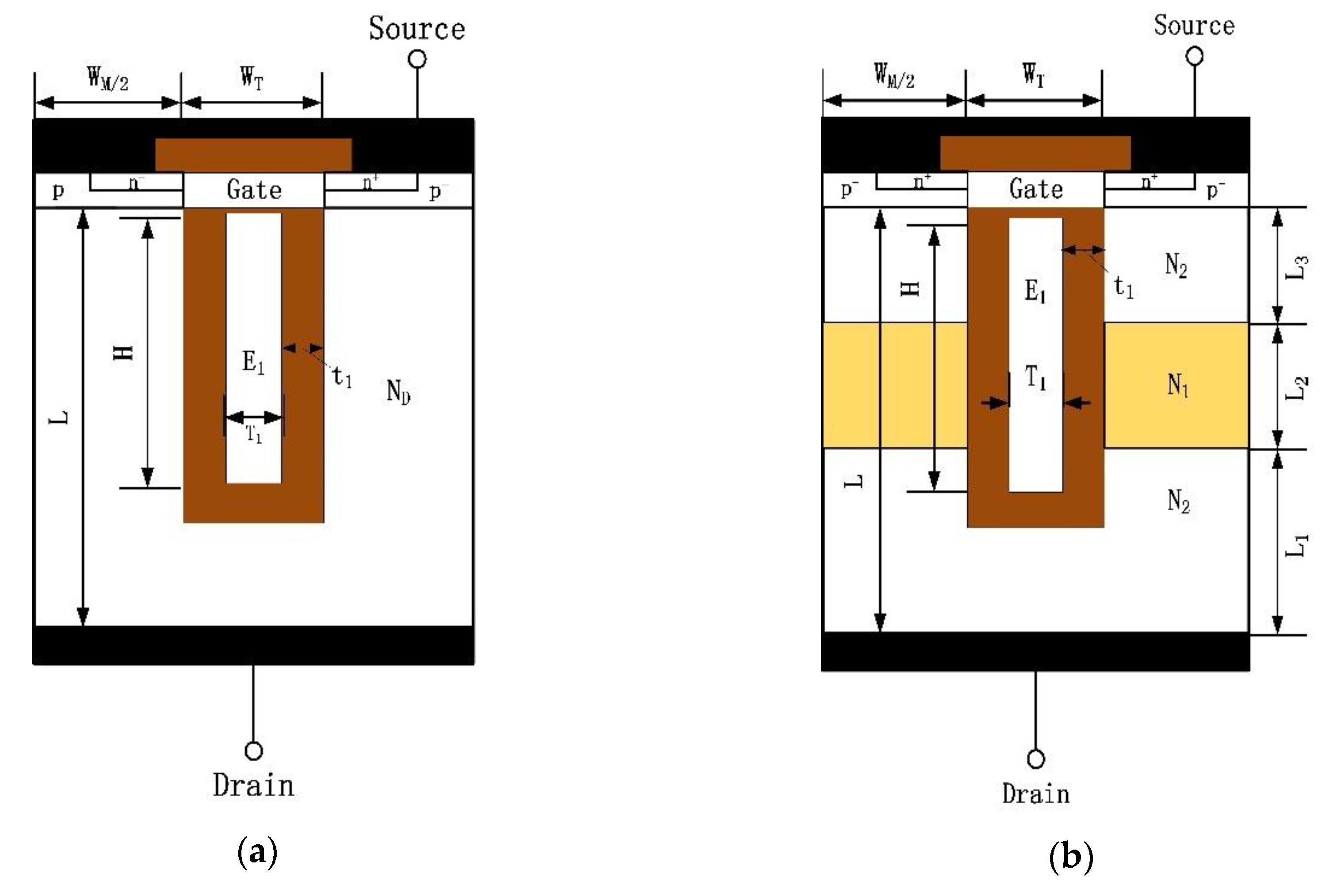
In order to achieve the desired charge-coupling, the split-gate electrode within the oxide coated trenches is designed to connect the source during operation in the blocking mode, as shown in Figure 1. The cross-sectional view of the HDSGRSO UMOSFET is presented in Figure 1b. Conventionally, the doping concentration of the n-drift is uniform. In this study, the epitaxial layer of HDGRSO UMOSFET has been divided into three parts with different doping concentration and thickness: the upper, the middle and lower epitaxial layers. The middle epitaxial layer has a higher doping concentration compared with the upper and lower epitaxial. In order to emphasize the modulation effect of the high doped epitaxial layer on the electric field, the doping concentrations of the upper and lower epitaxial layers are set to same, and the thickness of the high doped epitaxial layer is L2.
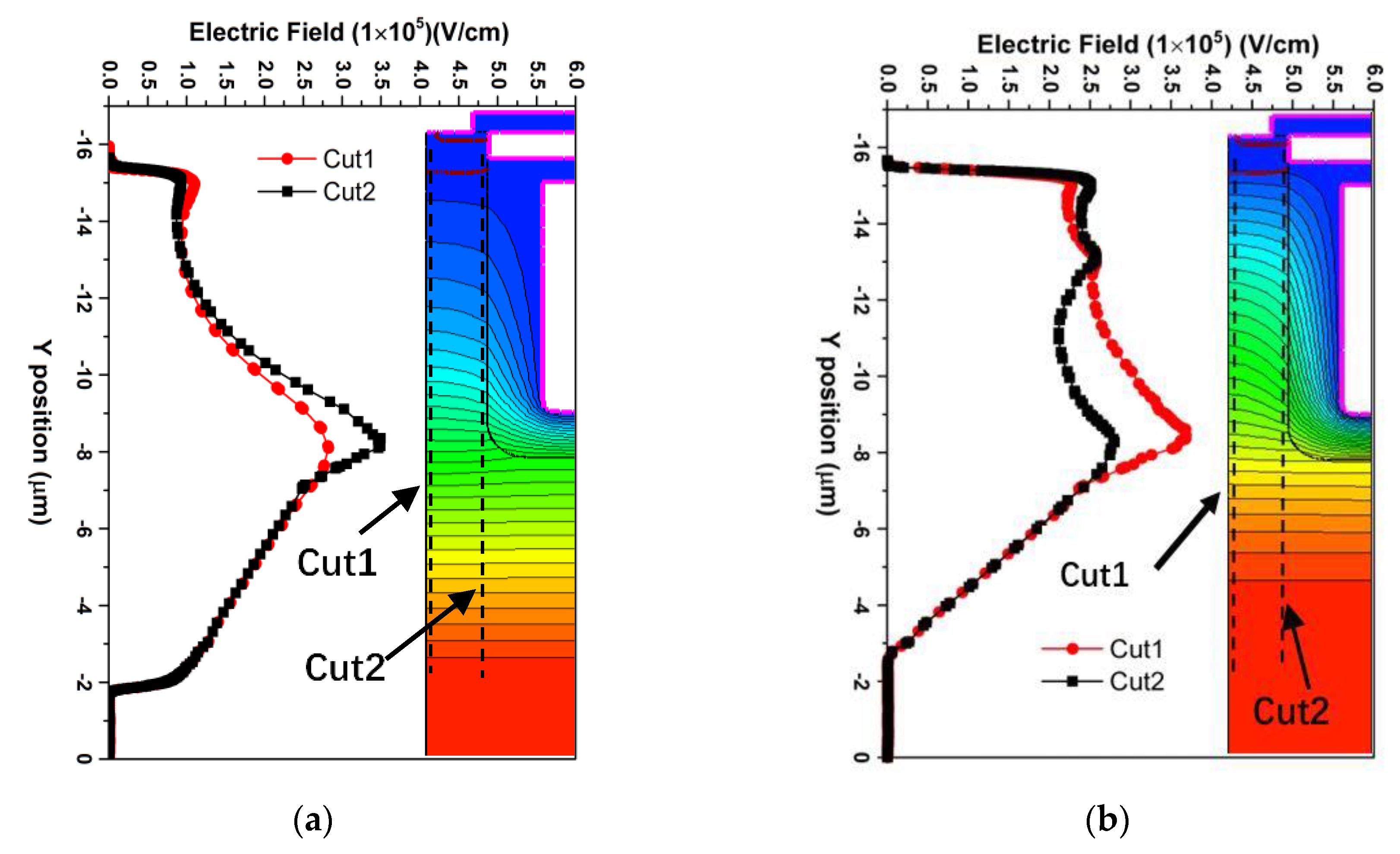
In this work, we used the TCAD to compare the performance of two structures. The potential contours and the electric field distribution along the trench surface (cut2) and in the middle of Mesa active area (cut1) for two structures at VDS = 240 V are represented as shown in the Figure 2. The doping concentration of the n-drift (ND and N2) was 1 × 10¹⁵/cm−3 and 5 × 10¹⁵/cm−3 for SGRSO and HDSGRSO UMOSFET, respectively, and the doping concentration of the high doped epitaxial layer was 1.5 × 10¹⁶/cm−3. It can be seen from the picture that the potential lines originally concentrated on the lower part moves to the upper part of the n-drift region, and the electric field of HDSGRSO UMOSFET distribution was more uniform than that of SGRSO UMOSFET. Furthermore, a small electric field peak appeared at the interface between the upper and the middle epitaxial layers, as shown in Figure 2, at −13.5 μm in the y-axis. Therefore, the high doped epitaxial layer can modulate the electric field distribution and reduce the internal high electric field to improve the BV.
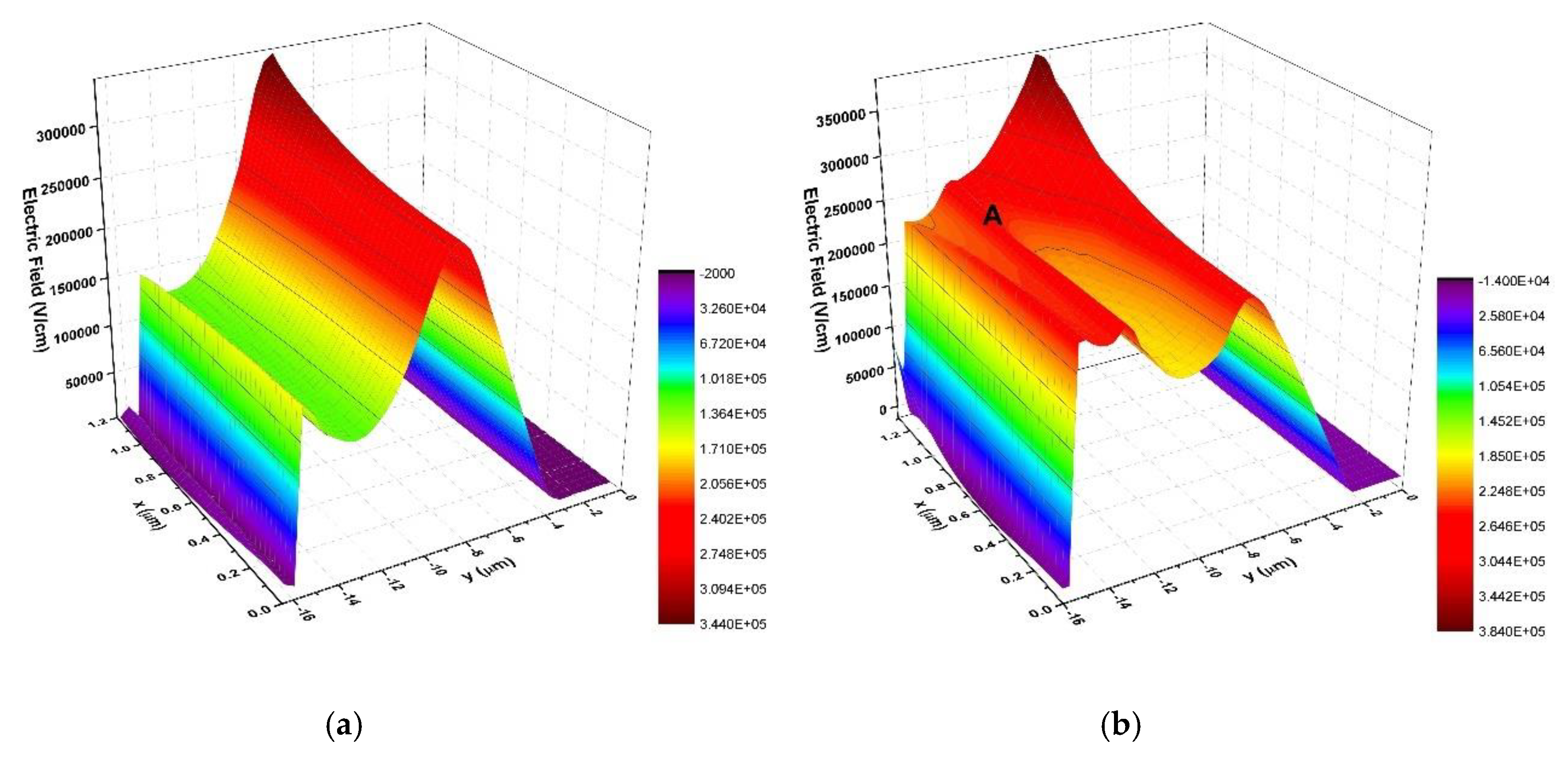
Figure 3 shows the three-dimensional view of the electric field distributions for two structures with the same n-drift doping concentration (ND and N2) 5 × 10¹⁵/cm−3. The small electric field peak (at point A) brought by the high doped epitaxial layer is shown in the Figure 3b. It is obvious that the electric field in the drift region of HDSGRSO UMOSFET is more uniform than that of the SGRSO UMOSFET at the same n-drift doping concentration, and the volume under the electric field curved surface of HDSGRSO UMOSFET is bigger contrast to the SGRSO UMOSFET. As a result, the BV of HDSGRSO UMOSFET is 240 V, while that of SGRSO UMOSFET is 190 V.
3. Fabrication Procedure
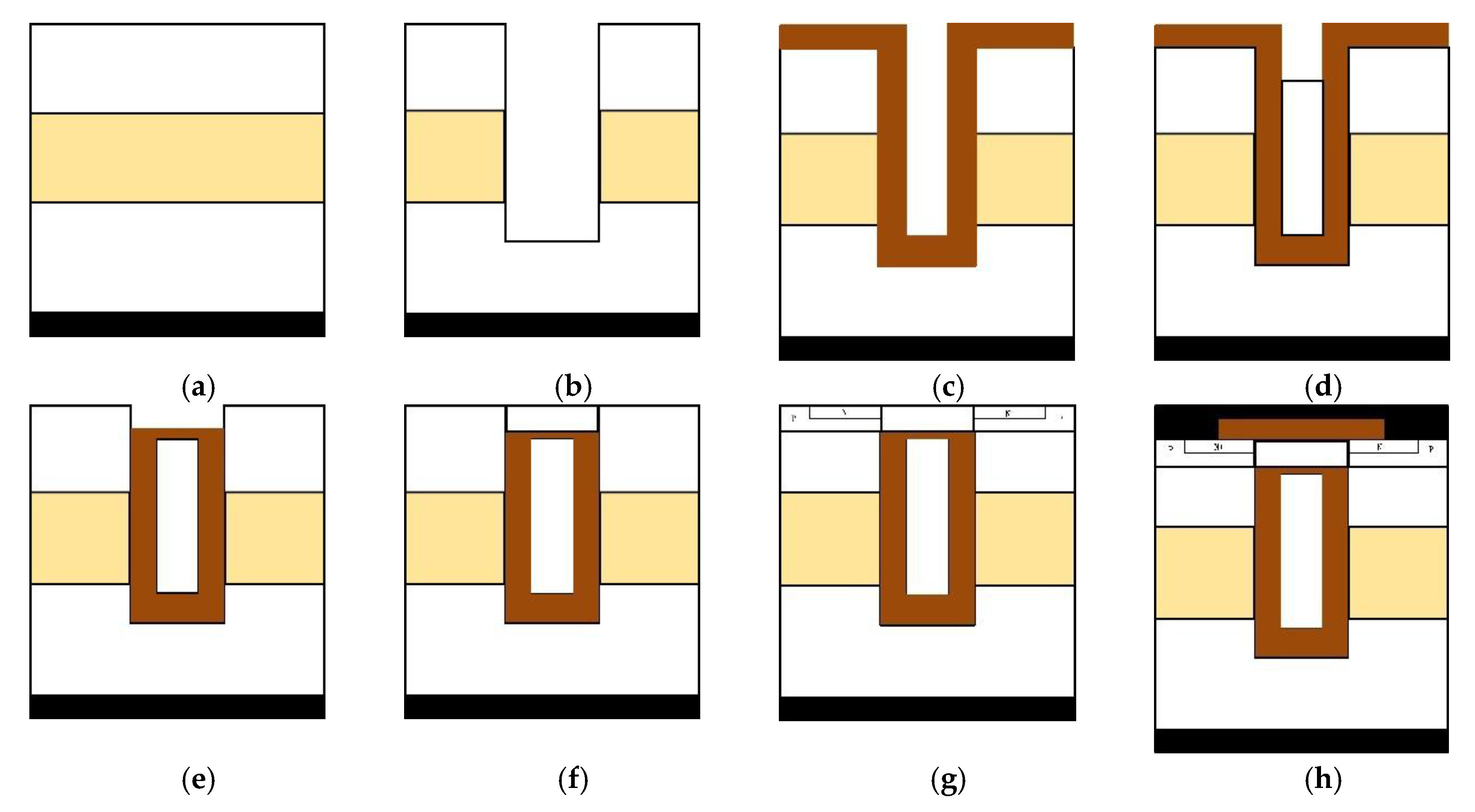
Figure 4 exhibits the fabrication process and structure of the HDSGRSO UMOSFET. The fabrication process of epitaxial layer is the only difference compared to traditional processes. First, a 3.2 μm n-type epitaxial layer is formed on the N+ substrate. Then, the middle and upper n-type epitaxial layer are formed on the first epitaxial in the same way. The doping concentration of the bottom and the upper epitaxial layers is the same, but the middle epitaxial layer has a higher doping concentration (a). Secondly, dry etching can be used to form the deep trench. An oxide layer is formed by thermally oxidized on the trench surface and then etched off to smooth the trench corner (b). Next, a 1.2 μm oxide is deposited to form the field oxide (c). Polysilicon is then deposited in the trench to form the source electrode which is surrounded by the field oxide (d). Afterwards, a thick oxide is deposited and etched back to separate the gate and the source electrode (e). Following, the gate oxide is formed by thermally oxidizing for 25 min under 1050 degrees dry oxygen conditions, and the polysilicon is deposited again to obtain the gate electrode (f). Subsequently, the p-body and n+ source region are formed by implanted ions, respectively (g). Finally, a thick oxide is deposited on the gate surface to separate the gate and source metallic electrodes, and then the fabrication of the device is finished (h).
4. Results and Discussion
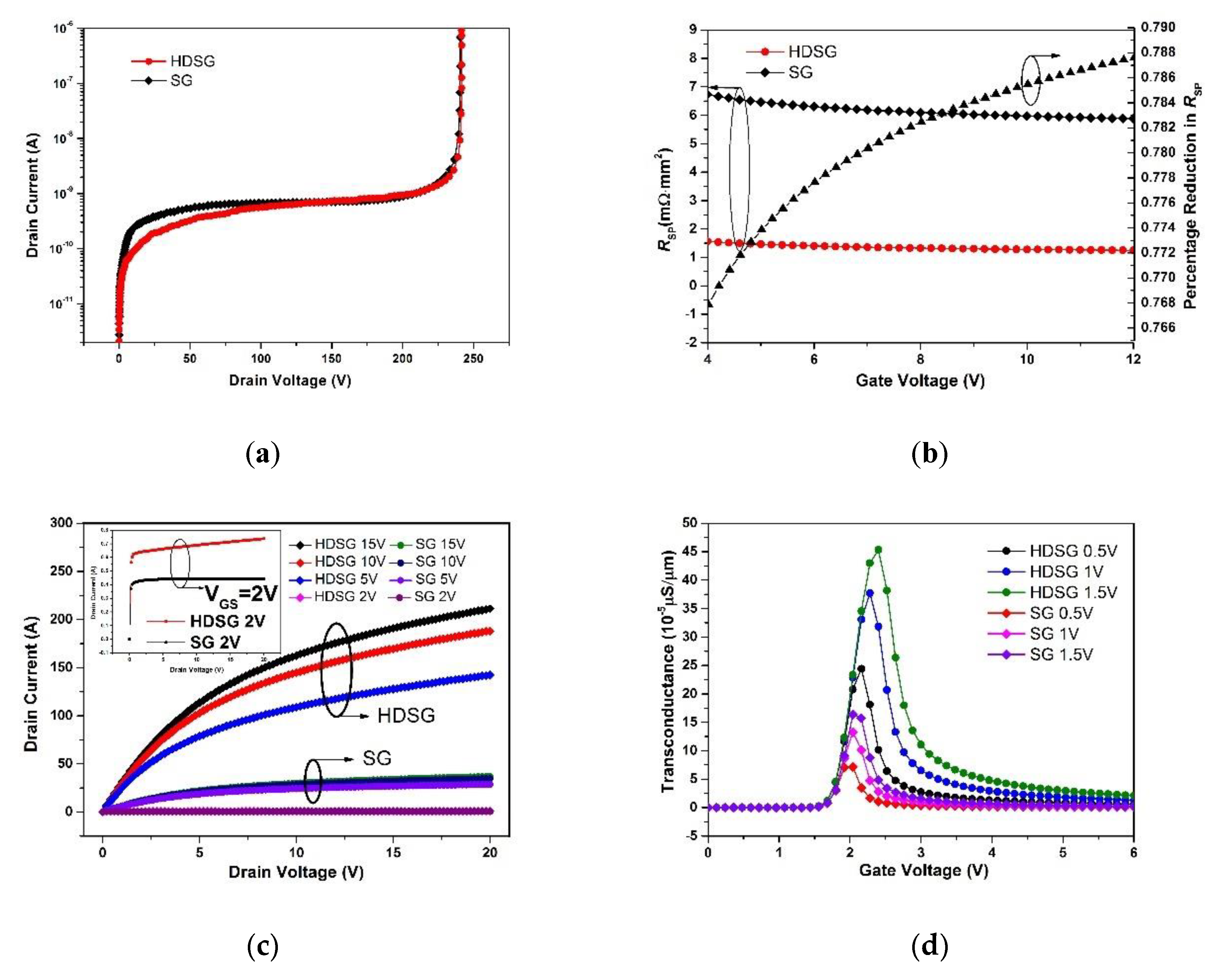
Figure 5 shows the characteristics of the SGRSO and HDSGRSO UMOSFETs for same bias condition; the structural parameters adopted in the simulations are shown in the Table 1. The breakdown voltage for the two structures is shown in the Figure 5a, and the limit of drain current density is 1 μA/μm2. It is obvious that the breakdown voltage of both is about 240 V. The relationship between the RSP and gate voltage is shown in the Figure 5b for the two structures at VDS = 0.3 V. It can be found that the RSP of the HDSGRSO UMOSFET is much smaller than that of the SGRSO UMOSFET, and the gap between them increases with the increase of the gate voltage. The RSP of the HDSGRSO UMOSFET can be reduced by 76%~79%, in contrast to the conventional structure at the same gate voltage.
The drain I-V characteristics of the SGRSO and HDSGRSO UMOSFETs with same bias condition are shown in Figure 5c when the breakdown voltage is 240 V. It is obvious that the HDSGRSO UMOSFET has a relatively large current than that of SGRSO UMOSFET when the VGS is 2 V, 5 V, 10 V and 15 V, respectively. Moreover, the current of the HDSGRSO UMOSFET when the VGS is 5 V even exceeds the current of the SGRSO UMOSFET at 15 V especially. The transconductance of HDSGRSO and SGRSO UMOSFETs is shown in the Figure 5d. It is similar to the output characteristics of the two structures that the transconductance of HDSGRSO UMOS at the VGS of 0.5 V is bigger than that of SGRSO UMOSFET when the VGS is 1.5 V. The transconductance of HDSGRSO UMOSFET increases by approximately 178% contrast to the SGRSO UMOSFET, when the VGS is 1.5 V.
An extensive analysis of the HDSGRSO UMOSFET has been given in contrast with SGRSO UMOSFET with the same structure parameters. The model of bandgap narrowing, concentration dependent mobility model, parallel electric field-dependent mobility model, Shockley-Read-Hall (SRH) model and impact-ionization model have been adopted in the simulation work [16].
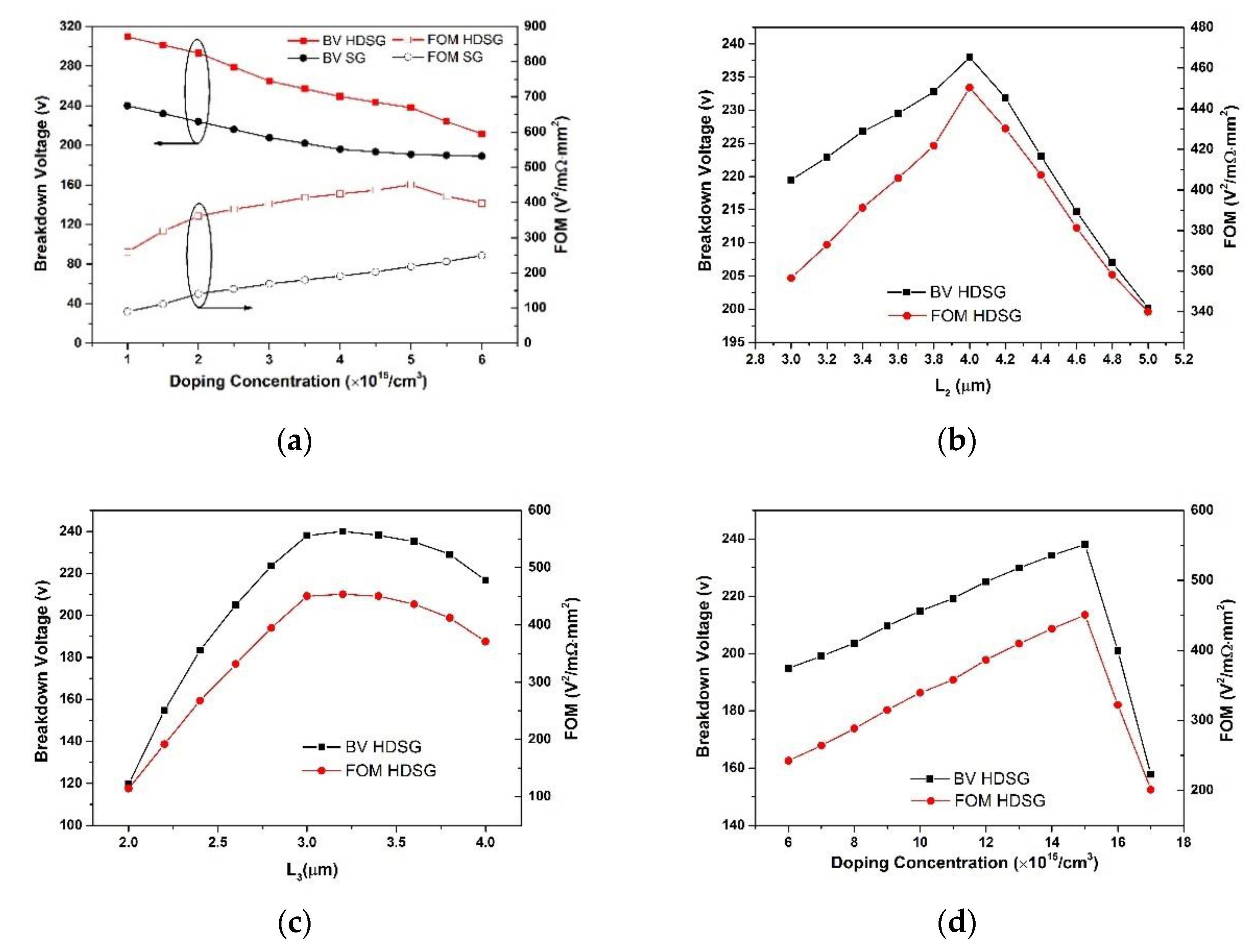
Figure 6a shows the BV and FOM (BV2/RSP) at different doping concentrations of the n-drift region. Table 1 shows the parameters we adopted in the simulations. The BV of the two structures increases with the decreasing of the doping concentration of n-drift within the range of the 1 × 10¹⁵/cm−3 −6 × 10¹⁵/cm−3. When the doping concentration of the drift region is 5 × 10¹⁵/cm−3, the FOM of HDSGRSO UMOSFET achieves the optimal value, which improved by 106% contrasted with the SGRSO UMOSFET, and the BV of HDSGRSO and SGRSO UMOSFETs were 239 V and 191 V respectively, which improved by 25.1%. It is worth noting that when the BV of the two structures was about 240 V, the FOM of HDSGRSO UMOSFET improved by 402% in contrast to the SGRSO UMOSFET as the doping concentration of the drift region is 5 × 10¹⁵/cm−3 and 1 × 10¹⁵/cm−3 for HDSGRSO and SGRSO UMOSFETs. The BV and FOM (BV2/RSP) at different widths of the doped layer L2 are shown in Figure 6b. It gets the optimal FOM and BV when the L2 is 4 μm. The BV and FOM (BV2/RSP) at different thickness of the upper n-drift (L3) is shown in Figure 6c when the L2 is 4 μm. It achieves the highest FOM and BV when L3 is 3.2 μm. Figure 6d shows the BV and FOM (BV2/RSP) at different doping concentrations of the high doped epitaxial layer when the n-drift region is 5 × 10¹⁵/cm−3. It is obvious the BV of the HDSGRSO UMOSFET is gradually increasing with the increase of the doping concentration of the high doped epitaxial layer. It gets optimal FOM and BV when the doping concentration of the high doped epitaxial layer is 1.5 × 10¹⁶/cm−3, because the modulation effect of the electric field in the n-drift gradually increases and reaches the optimal level with the increasing of the doping concentration of high doped epitaxial layer. However, when the doping concentration of the middle epitaxial layer is higher than 1.5 × 10¹⁶/cm−3, the charge balance in the n-drift will be broken and the BV will drop steeply.
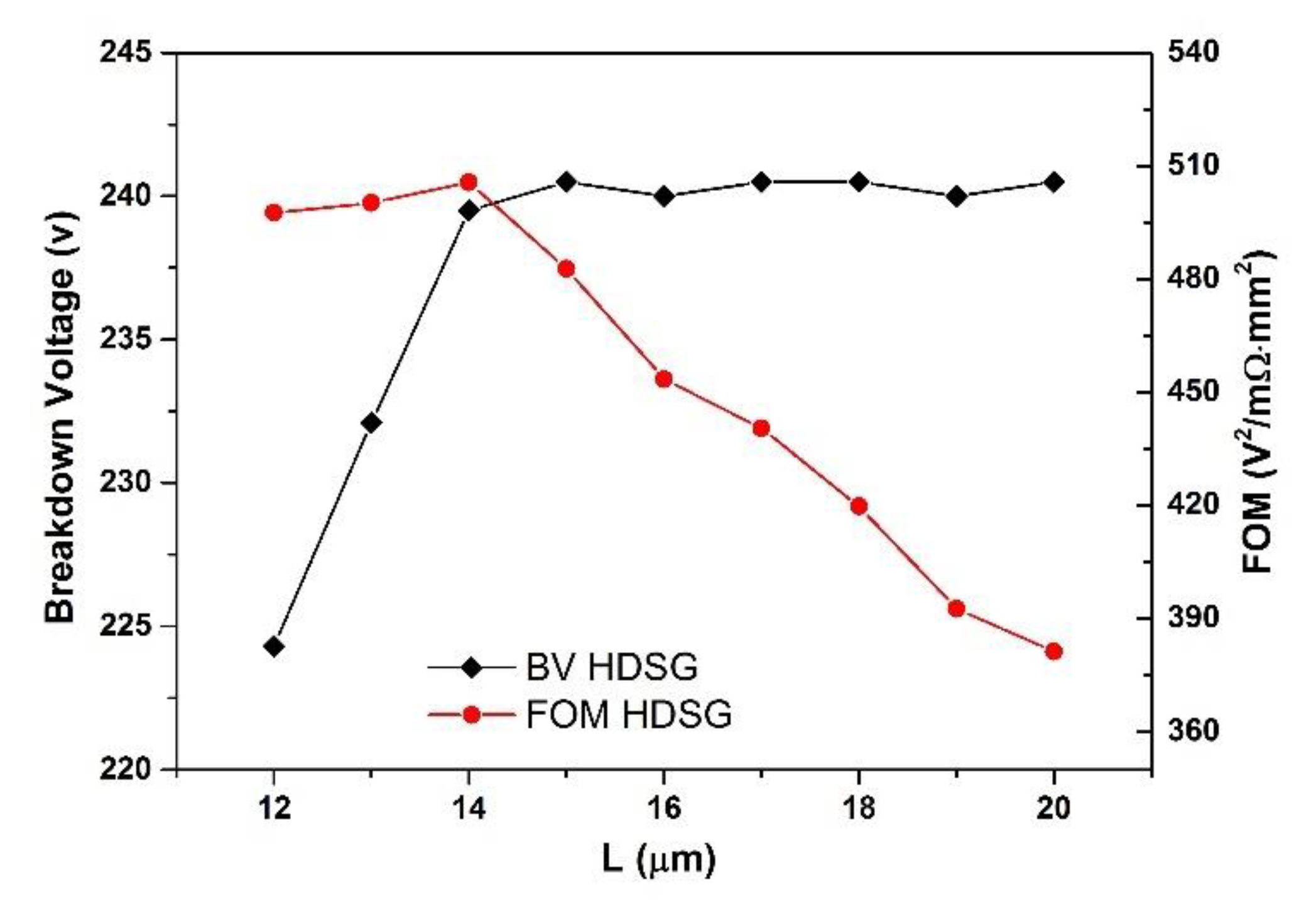
Figure 7 shows the BV and FOM (BV2/RSP) at different thicknesses of the drift region. It indicates that there exists a saturated BV at a certain thickness. When the L is 14 μm, the FOM value and BV reaches the optimal value, respectively, and the BV is about 240 V. With the increase of epitaxial thickness, the RSP gradually increases, resulting in the decrease of FOM. The L is 14 μm for HDSGRSO UMOSFET, whereas the L’ is 16 μm for SGRSO UMOSFET when the BV is 240 V. Because of the enhancing of the electric field by high doped epitaxial layer, the breakdown occurs before the n-drift is depleted completely. Therefore, it can reduce the thickness of the epitaxial layer and RSP. As a result, the FOM has been increased by 464% as compared with the SGRSO UMOSFET when the BV is about 240 V, according to the simulation results.
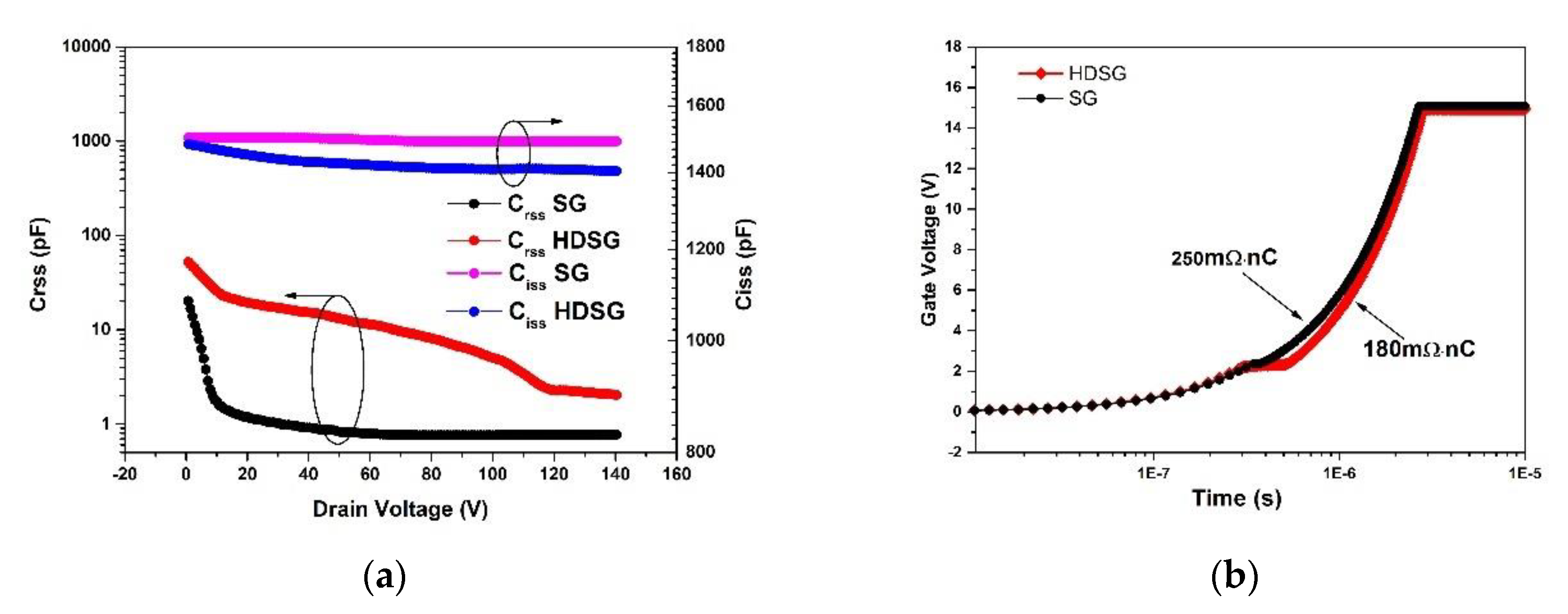
For the power MOSFET used in the high frequency field, the switching losses is the most important part of the total power loss. The time period associated with the increase of the drain current and decrease of the drain voltage is determined by the charging of the device capacitances. The Figure 8a shows the input capacitances (Ciss) and reverse transfer capacitances (Crss) of both structures when VGS = 0 V and f = 1 MHz. The Crss of the HDSGRSO UMOSFET has a slight increase in comparison with the ordinary structure because of the highly doped epitaxial layer. However, the capacitances difference between the two structures is gradually reduced as the drain voltage increases. When the drain voltage exceeds 120 V, the Crss of the two structures are almost same. The Crss of HDSGRSO and SGRSO UMOSFETs is 2 pF and 0.8 pF, respectively, at VDS = 140 V. On the other hand, the doping concentration of the p-body is slightly reduced under the same boron dose due to the highly doped epitaxial layer, which causes a slight reduction of the Ciss for HDSGRSO UNOSFET. It can be seen that the HDSGRSO UMOSFET has lower Ciss contrast to the SGRSO UNOSFET when the drain voltage increases from 0 to 140 V. The Ciss of HDSGRSO and SGRSO UMOSFETs is 1400 pF and 1490 pF, respectively, at VDS = 140 V, which is of benefit to improve the switching speed of the HDSGRSO UMOSFET. The FOMs of RSP × Qgd have been adopted to compare the dynamic characteristics of two structures. The FOM (RSP × Qgd) of HDSGRSO and SGRSO UMOSFETs is 180 and 250 mΩ∙nC, as shown in the Figure 8b. The FOM of devices with high doped epitaxial layer structure was reduced by 27.9% in contrast to SGRSO UMOSFET because the introduction of the high doped epitaxial layer increases the doping concentration in the drift region, which makes the RSP decrease greatly.
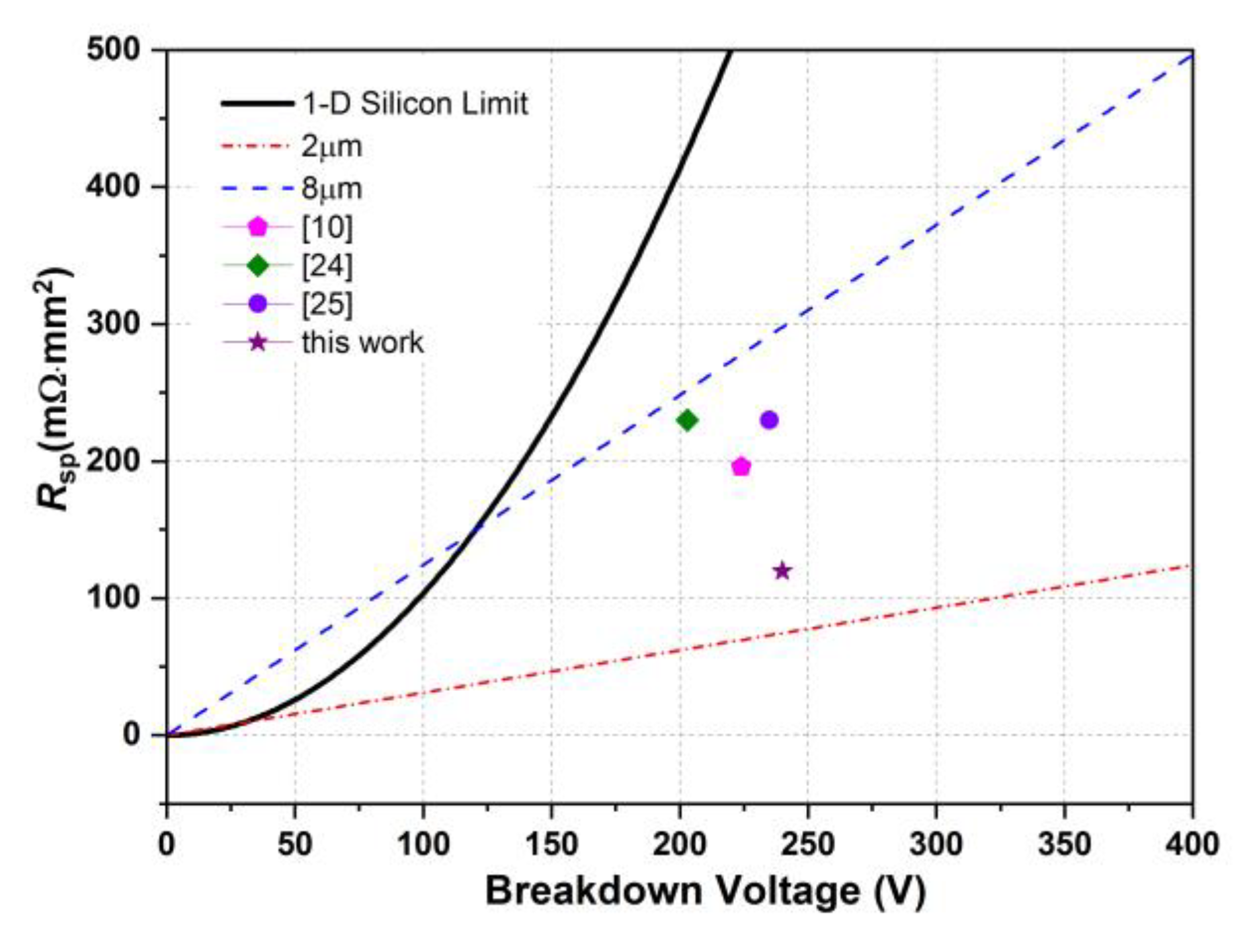
Table 2 shows the switching time and switching energy loss of two structures at 120 V, 4 A. The HDSGRSO UMSOFET has a lower turn-on delay time (td(on)) because of the smaller input capacitance, however, the rise time(tr) of the HDSGRS UMOSFET is slightly higher due to the larger Crss, which causes results in the turn-on loss (Eon) to be very close. On the other hand, the lager Crss causes a certain increase of the turn-off delay (td(off)) time and fall time (tf), which leads to an increase of turn-off loss (Eoff) in contrast to the SGRSO UMOSFET, and this needs more research in the future. The performance of the HDSGRSO UMOSFET has been compared with the one-dimensional silicon limit and other works in Figure 9. The HDSGRSO UMOSFET has the lowest RSP and the highest BV compared with the previous power UMOSFETs.
5. Conclusions
In this article, a split-gate resurf stepped oxide with high doped epitaxial layer (HDSGRSO) UMOSFET has been proposed. The epitaxial layer of HDGRSO UMOSFET has been divided into three parts: the upper epitaxial layer, the lower epitaxial layer and the middle epitaxial layer with higher doping concentration. The TCAD simulation results show that the RESURF active has been enhanced due to the high doped epitaxial layer, which can modulate the distribution of the electric field and reduce the internal high electric field. As a result, the BV of HDGRSO UMOSFET has been improved greatly. Meanwhile, the n-drift region has a higher doping concentration due to the high doped epitaxial layer, which can reduce the RSP for a given BV. Therefore, the FOM of the device with high doped epitaxial can be improved significantly. According to the simulation results, the FOM (BV2/RSP) of HDSGRSO UMOSFET has been improved by 464%, and FOM (RSP × Qgd) of HDSGRSO UMOSFET has been reduced by 27.9% compared to the conventional structure, respectively, when the BV is 240 V. Furthermore, the only difference between this procedure and the traditional procedure is the fabrication of the epitaxial layer, and no extra special process is required in this advanced fabrication procedure, which is relatively cost-effective and achievable.
Author Contributions
Conceptualization, R.C. and L.W.; methodology, R.C.; software, H.Z.; validation, R.C. and L.W.; formal analysis, R.C.; investigation, M.G.; resources, L.W.; data curation, R.C.; writing—original draft preparation, R.C.; writing—review and editing, L.W.; visualization, M.C.; supervision, L.W.; project administration, L.W.; funding acquisition, L.W. All authors have read and agreed to the published version of the manuscript.
Funding
This research received no external funding.
Conflicts of Interest
The authors declare no conflict of interest.
References
- Shi, L.; Fan, X.; Miao, Z.; Wang, P.; Shen, K.; Yao, L. A technique for fabricating low voltage charge-coupled mosfet with 0.9 UM pitch size. In Proceedings of the China Semiconductor Technology International Conference, Shanghai, China, 11–12 March 2018. [Google Scholar]
- Kang, H.; Udrea, F. Theory of 3-D Superjunction MOSFET. IEEE Trans. Electron Devices 2019, 66, 5254–5259. [Google Scholar] [CrossRef]
- Ye, Z.Y.; Liu, L.; Yao, Y.; Lin, M.Z.; Wang, P.F. Fabrication of a 650V Superjunction MOSFET With Built-in MOS-Channel Diode for Fast Reverse Recovery. IEEE Electron Device Lett. 2019, 40, 1159–1162. [Google Scholar] [CrossRef]
- Kang, H.; Udrea, F. Analytic Model of Specific ON-State Resistance for Superjunction MOSFETs with an Oxide Pillar. IEEE Electron Device Lett. 2019, 40, 761–764. [Google Scholar] [CrossRef]
- Baliga, B.J. Vertical Field Effect Transistors Having Improved Breakdown Voltage Capability and Low On-State Resistance. U.S. Patent 5637898A, 10 June 1997. [Google Scholar]
- Koops, G.E.J.; Hijzen, E.A.; Hueting, R.J.E.; Zandt, M.A.A. RESURF stepped oxide (RSO) MOSFET for 85V having a record-low specific on-resistance. In Proceedings of the 16th International Symposium on Power Semiconductor Devices and ICs, Kitakyushu, Japan, 24–27 May 2004; pp. 185–188. [Google Scholar]
- Gajda, M.A.; Hodgskiss, S.W.; Mounfield, L.A.; Irwin, N.T.; Koops, G.E.J.; van Dalen, R. Industrialisation of Resurf Stepped Oxide Technology for Power Transistors. In Proceedings of the IEEE International Symposium on Power Semiconductor Devices and IC’s, Naples, Italy, 4–8 June 2006; pp. 1–4. [Google Scholar]
- Goarin, P.; Koops, G.E.J.; van Dalen, R.; Cam, C.L.; Saby, J. Split-gate Resurf Stepped Oxide (RSO) MOSFETs for 25V applications with record low gate-to-drain charge. In Proceedings of the 19th International Symposium on Power Semiconductor Devices and IC’s, Jeju Island, Korea, 27–31 May 2007; pp. 61–64. [Google Scholar]
- Tong, C.F.; Cortes, I.; Mawby, P.A.; Covington, J.A. Static and Dynamic Analysis of Split-Gate RESURF Stepped Oxide (RSO) MOSFETs for 35 V Applications. In Proceedings of the Conference on Electron Devices, Santiago de Compostela, Spain, 11–13 February 2009. [Google Scholar]
- Park, C.; Azam, M.; Dengel, G.; Shibib, A.; Terrill, K. A New 200 V Dual Trench MOSFET With Stepped Oxide for Ultra Low RDS(on). In Proceedings of the 31st International Symposium on Power Semiconductor Devices and ICs, Shanghai, China, 19–23 May 2019; pp. 95–98. [Google Scholar]
- Baliga, B.J.; North Carolina State University. Power Semiconductor Devices Having Improved High Frequency Switching and Breakdown Characteristics. U.S. Patent 5,998,833, 7 December 1999. [Google Scholar]
- Wang, Y.; Hu, H.; Jiao, W. Split-Gate-Enhanced UMOSFET with an Optimized Layout of Trench Surrounding Mesa. IEEE Trans. Electron Devices 2012, 59, 3037–3041. [Google Scholar] [CrossRef]
- Wang, Y.; Lan, H.; Cao, F.; Liu, Y.-T.; Shao, L. A novel power UMOSFET with a variable K dielectric layer. Chin. Phys. Soc. 2012, 21, 569–572. [Google Scholar] [CrossRef]
- Wang, Y.; Hu, H.F.; Yu, C.H.; Lan, H. High-performance split-gate enhanced UMOSFET with p-pillar structure. IEEE Trans. Electron Devices 2013, 60, 2302–2307. [Google Scholar] [CrossRef]
- Wang, Y.; Lan, H.; Dou, Z.; Hu, H.F. Method to improve trade-off performance for split-gate power U-shape metal-oxide semiconductor field-effect transistor with compound trench dielectrics. IET Power Electron. 2014, 7, 2030–2034. [Google Scholar]
- Wang, Y.; Hu, H.F.; Zheng, D.; Yu, C.H. Way of operation to improve performance for advanced split gate resurf stepped oxide UMOSFET. IET Power Electron. 2014, 7, 2964–2968. [Google Scholar] [CrossRef]
- Wang, Y.; Hu, H.F.; Yu, C.-H.; Wei, J.-T. Advanced hexagonal layout design for split-gate reduced surface field stepped oxide U-groove metal–oxide–semiconductor field-effect transistor. IET Power Electron. 2015, 8, 678–684. [Google Scholar]
- Park, C.; Havanur, S.; Shibib, A.; Terrill, K. 60 V rating split gate trench MOSFETs having best-in-class specific resistance and Figure-of-merit. In Proceedings of the 28th International Symposium on Power Semiconductor Devices and ICs, Prague, Czech Republic, 12–16 June 2016; pp. 387–390. [Google Scholar]
- Wang, Y.; Yu, C.; Li, M.; Cao, F.; Liu, Y. High-Performance Split-Gate-Enhanced UMOSFET with Dual Channels. IEEE Trans. Electron Devices 2017, 64, 1455–1460. [Google Scholar] [CrossRef]
- Kobayashi, K.; Kato, H.; Nishiguchi, T.; Shimomura, S.; Ohno, T.; Nishiwaki, T.; Aida, K.; Ichinoseki, K.; Oasa, K.; Kawaguchi, Y. 100-V Class Two-step-oxide Field-Plate Trench MOSFET to Achieve Optimum RESURF Effect and Ultralow On-resistance. In Proceedings of the 31st International Symposium on Power Semiconductor Devices and ICs, Shanghai, China, 19–23 May 2019; pp. 99–102. [Google Scholar]
- Baliga, B.J. Advanced Power MOSFET Concepts; Springer Science and Business Media: New York, NY, USA, 2010. [Google Scholar]
- Baliga, B.J. Trends in power discrete devices. In Proceedings of the 10th International Symposium on Power Semiconductor Devices and ICs, Kyoto, Japan, 3–6 June 1998; pp. 5–10. [Google Scholar]
- Wang, Y.; Hu, H.; Jiao, W. High-Performance Gate-Enhanced Power UMOSFET with Optimized Structure. IEEE Electron Device Lett. 2010, 31, 1281–1283. [Google Scholar] [CrossRef]
- Hattori, Y.; Nakashima, K.; Kuwahara, M.; Yoshida, T.; Yamauchi, S.; Yamaguchi, H. Design of a 200V Super Junction MOSFET with n-buffer regions and its Fabrication by Trench Filling. In Proceedings of the International Symposium on Power Semiconductor Devices and ICs, Kitakyushu, Japan, 24–27 May 2004; pp. 189–192. [Google Scholar]
- Shibata, T.; Noda, Y.; Yamauchi, S.; Nogami, S.; Yamaoka, T.; Hattori, Y.; Yamaguchi, H. 200V Trench Filling Type Super Junction MOSFET with Orthogonal Gate Structure. In Proceedings of the 19th International Symposium on Power Semiconductor Devices and IC’s, Jeju Island, Korea, 27–31 May 2007; pp. 37–40. [Google Scholar]
Figure 1.
Cross section view of (a) split-gate resurf stepped oxide (SGRSO) and (b) split-gate resurf stepped oxide with high doped epitaxial layer (HDSGRSO) u-shape metal oxide semiconductor field effect transistor (UMOSFET).
Figure 1.
Cross section view of (a) split-gate resurf stepped oxide (SGRSO) and (b) split-gate resurf stepped oxide with high doped epitaxial layer (HDSGRSO) u-shape metal oxide semiconductor field effect transistor (UMOSFET).

Figure 2.
Potential distribution and electric field from cutlines comparing of the (a) SGRSO and (b) HDSGRSO UMOSFET at VDS = 240 V.
Figure 2.
Potential distribution and electric field from cutlines comparing of the (a) SGRSO and (b) HDSGRSO UMOSFET at VDS = 240 V.

Figure 3.
The three dimensions view of electric field distributions for the (a) SGRSO and (b) HDSGRSO UMOSFET with the same n-drift region doping concentration (ND and N2) 5 × 10¹⁵/cm−3.
Figure 3.
The three dimensions view of electric field distributions for the (a) SGRSO and (b) HDSGRSO UMOSFET with the same n-drift region doping concentration (ND and N2) 5 × 10¹⁵/cm−3.

Figure 4.
Fabrication procedure of the HDSGRSO UMOSFET.(a) Epitaxial layers are formed, (b) Trench is opened, (c) Thick oxide is deposited, (d) Polysilicon is deposited and etched back, (e) Thick oxide is deposited and etched back, (f) Gate oxide and gate poly are formed, (g) The p-body and n+ source region are formed, (h) Thick oxide and source metal are deposited.

Figure 5.
Drain I-V characteristics: (a) Breakdown Voltage (BV); (b) RSP at different gate voltage with VDS = 0.3 V and percentage reduction in RSP as compared with the SGRSO UMOSFET; (c) output characteristics and (d) transconductance of two structures.
Figure 5.
Drain I-V characteristics: (a) Breakdown Voltage (BV); (b) RSP at different gate voltage with VDS = 0.3 V and percentage reduction in RSP as compared with the SGRSO UMOSFET; (c) output characteristics and (d) transconductance of two structures.

Figure 6.
BV and FOM (BV2/RSP) at different (a) doping concentration of n-drift region; (b) L2 (height of high doped epitaxial layer); (c) L3 and (d) doping concentration of high doped epitaxial layer for HDSGRSO UMOSFET.
Figure 6.
BV and FOM (BV2/RSP) at different (a) doping concentration of n-drift region; (b) L2 (height of high doped epitaxial layer); (c) L3 and (d) doping concentration of high doped epitaxial layer for HDSGRSO UMOSFET.

Figure 7.
BV and FOM (BV2/RSP) of HDSGRSO UMOSFET at different n-drift region thickness.

Figure 8.
The Crss and Ciss (BV2/RSP) at different drain voltage (a) and (b) comparison of gate charge and RSP × Qgd for HDSGRSO and SGRSO UMOSFETs.
Figure 8.
The Crss and Ciss (BV2/RSP) at different drain voltage (a) and (b) comparison of gate charge and RSP × Qgd for HDSGRSO and SGRSO UMOSFETs.

Figure 9.
Performance comparing of one-dimensional silicon limit, two-dimensional charge-coupling limits for the pitches of 2 and 8 μm. Some references are [10,24,25] and this work.


Table 1.
Structural parameters adopted in the simulations.
| Parameter | Value |
|---|---|
| Trench depth (HT) | 7.5 μm |
| Gate depth(HG) | 1.0 μm |
| n+ source junction depth | 0.2 μm |
| p- body junction depth | 0.8 μm |
| p- body doping concentration | 1.5 × 1018 cm−3 |
| Trench width (WT) | 3.6 μm |
| Mesa Width (WM) | 3.2 μm |
| Width of E1 (T1) | 1.6 μm |
| Thickness of field oxide (t1) | 1.2 μm |
| n-drift region doping concentration (ND) | 1 × 1015 cm−3 |
| Doping of lower epitaxial layer (N2) | 5 × 1015 cm−3 |
| Doping of middle epitaxial layer (N1) | 1.5 × 1016 cm−3 |
| Doping of upper epitaxial layer (N2) | 5 × 1015 cm−3 |
| Thickness of gate oxide | 50 nm |
| Thickness of n- drift region (L) | 16 μm |
| Thickness of lower epitaxial layer (L1) | 3.2 μm |
| Thickness of middle epitaxial layer (L2) | 4 μm |
| Thickness of upper epitaxial layer (L3) | 8.8 μm |
| Height of source electrode of SGRSO (H) | 6.3 μm |
Table 2.
Switching time and switching energy loss of two structures.
| td(on) (ns) | td(off) (ns) | tr (ns) | tf (ns) | Eon (μJ) | Eoff (μJ) | |
|---|---|---|---|---|---|---|
| SGRSO | 0.59 | 7.57 | 0.57 | 5.59 | 0.081 | 0.92 |
| HDSGRSO | 0.48 | 7.93 | 0.69 | 17.64 | 0.082 | 1.78 |
Publisher’s Note: MDPI stays neutral with regard to jurisdictional claims in published maps and institutional affiliations. |
© 2020 by the authors. Licensee MDPI, Basel, Switzerland. This article is an open access article distributed under the terms and conditions of the Creative Commons Attribution (CC BY) license (http://creativecommons.org/licenses/by/4.0/).
Share and Cite
MDPI and ACS Style
Chen, R.; Wang, L.; Zhang, H.; Cui, M.; Guo, M. A New Split Gate Resurf Stepped Oxide UMOSFET Structure with High Doped Epitaxial Layer for Improving Figure of Merit (FOM). Appl. Sci. 2020, 10, 7895. https://doi.org/10.3390/app10217895
AMA Style
Chen R, Wang L, Zhang H, Cui M, Guo M. A New Split Gate Resurf Stepped Oxide UMOSFET Structure with High Doped Epitaxial Layer for Improving Figure of Merit (FOM). Applied Sciences. 2020; 10(21):7895. https://doi.org/10.3390/app10217895
Chicago/Turabian StyleChen, Runze, Lixin Wang, Hongkai Zhang, Mengyao Cui, and Min Guo. 2020. "A New Split Gate Resurf Stepped Oxide UMOSFET Structure with High Doped Epitaxial Layer for Improving Figure of Merit (FOM)" Applied Sciences 10, no. 21: 7895. https://doi.org/10.3390/app10217895
Note that from the first issue of 2016, this journal uses article numbers instead of page numbers. See further details here.