Novel sensor developments for photon science at the MPG semiconductor laboratory
 J. Ninkovic
 A. Bähr
 R. H. Richter
 J. Treis
- Semiconductor Laboratory of the Max-Planck-Society, Munich, Germany
The world of photon science experiences significant advancements since the advent of synchrotron light sources with unprecedented brilliance, intensity and pulse repetition rates, with large implications on the detectors used for instrumentation. Here, an overview about the work on this field carried out at the semiconductor laboratory of the Max-Planck-Society (MPG HLL) is given. Main challenges are high dynamic range to resolve faint features at the fringes of scatter images as well as structures in bright peaks, and high bandwidth to fully exploit the fast timing capability of the source. A newly developed device to improve the signal-to-noise-ratio (SNR) at high bandwidths is the so-called MARTHA (Monolithic Array of Reach-Through Avalanche Photodiodes) structure, which integrates an array of APDs on a monolithic substrate. The reach-through architecture assures near 100% fill factor and allows implementing a thin entrance window with optimized quantum efficiency for low energy X-rays. The structures operate in proportional mode with adjustable gain, and can serve as a drop-in replacement for PAD detectors in hybrid pixel systems. A more sophisticated solution for low to medium frame rate applications with high contrast requirement are pnCCDs with high dynamic range in the pixel area featuring DEPFET based readout nodes with non-linear amplification (NLA). The high dynamic range mode has been demonstrated for pnCCD devices with a pixel size down to 75 μm2. Framerates of up to 1 kHz are possible for a 1 Megapixel detector. Small size prototypes of these structures have recently been manufactured. Modified DEPFET structures with build-in non-linear amplification are also used to implement active pixel detectors optimized for high dynamic range. Successfully prototyped for the DSSC sensors (DEPFET Sensor with Signal Compression) at the XFEL, these structures are increasingly being used in applications requiring high contrast and intensity, e.g., TEM imaging. Charge handling capability and output characteristics can be tailored to the requirements, as well as pixel geometry and size. The large intrinsic gain of the DEPFET provides excellent SNR even at fast timing. Pixels can be read with a speed of 100 ns, the resulting frame rate depends on the degree of readout parallelization.
1 Introduction
Many applications in photon science involve x-ray scattering experiments using high intensity x-ray pulses. The images thus generated are characterized by a distribution of high intensity, small size spots or speckles, surrounded by “halo” regions with an intensity rapidly declining with the distance from the intensity peaks. In this context, intensity is usually measured as number of photons with a fixed energy. Relevant information about the scattering process is not only contained in the distribution and size of the peaks, but also in the details and shape of the intensity distribution within the halos down to their fringe. Measurements at lower intensity, however, are often limited by the suppression of low signal amplitudes, driven by the necessity of noise discrimination. An ideal detector system therefore needs to acquire the complete scattering image, from the highest peak intensity to the faintest halo regions, ideally down to single photons, and still maintain robust noise suppression efficiency.
Key performance parameters of detector systems for photon science instrumentation are the charge handling capacity (CHC) of the detector resolution elements and the dynamic range of the system. In this context, CHC is the maximum amount of signal charge the system is able to handle per resolution element (pixel) without loss or deterioration of information. High CHC is required to suppress blooming or spillover effects compromising the imaging performance up to the requested maximum signal charge, so the scattering patterns can be imaged correctly.
As imaging of both low and high intensity regions of the image are equally important, an optimization of the dynamic range needs to target both, the high and the low dynamic range limit. Concerning the high dynamic range limit, the maximum preamplifier output needs to fit the maximum required signal charge. When optimizing the low end of the dynamic range, the gain characteristics of the detector/preamplifier structure have to be modified in order to push the low dynamic range limit to the minimum value achievable for the given noise conditions. To optimize both, the maximum dynamic range and its low range detection limit, a system with multilinear or non-linear behavior of the detector-preamplifier combo is superior compared to conventional single gain approaches.
Another requirement arising from the high rate capability of contemporary X-ray sources is the requested high readout speed. The frame rates required for megapixel sized detector arrays range from several kHz up to the MHz range. This brings about fast detector readout, high bandwidth of the amplifiers, and fast processing of the acquired data in the data acquisition backend.
Any optimization of a detector system for photon science therefore needs to target the detector structure itself as well as the respective readout electronics. Focus hereby lies on the optimization of the dynamic range, the signal-to-noise ratio and the increase of readout speed.
In the following, an overview about the work on this field carried out at the semiconductor laboratory of the Max-Planck-Society (MPG HLL) is given.
2 Gain characteristics of photon science detectors
Photon science experiments, e.g., in X-ray scattering, use photons of fixed energy to illuminate a scattering target. In the following, the interrelation between signal, gain, noise, accuracy and dynamic range of such a detector is outlined by means of a model for an ideal detector. For the sake of simplicity, the model neglects the effects of charge sharing between pixels, although in reality they greatly influence the sensitivity for lower amplitudes.
2.1 Signal and detector model
Using the simplification mentioned above, the stimulus
The experimental requirement states that each pixel is able to record the signal from a maximum number of
where
A system matched to the requirements has a maximum pixel stimulus of
is a useful definition for the dynamic range as relevant figure of merit. The value of
To understand the connection, an idealized model detector system is considered, which converts the stimulus
In the application, a calibration function is used to retrieve a reconstructed value
To define the actual gain function, the most straightforward approach is that of a linear gain function of the form
being the optimal gain matched to the required dynamic range. In this approach,
with
The alternative approach investigated here is the square-root shaped gain function of the form.
which, in the following, is referred to as nonlinear gain function. This approach is chosen as an educated guess, because higher gain for lower amplitudes lifts the output signal above the noise threshold for yet smaller input stimuli. Accordingly, this yields a second degree polynomial without linear term for the calibration function:
with
Using these gain functions, expressions for the accuracy functions, low energy limit, dynamic range and single photon sensitivity limit were derived. Here, an ideal calibration (i.e.,
2.2 Comparison
For the gain functions and conditions sketched above, the model gives a set of relations describing the relevant performance parameters of the model detector. Table 1 compares some of the findings for the performance characteristics for the nonlinear and linear gain function. For a more compact notation, the definitions in the table use the term
which corresponds to the ratio of the output dynamic range to the noise of the preamplifier.
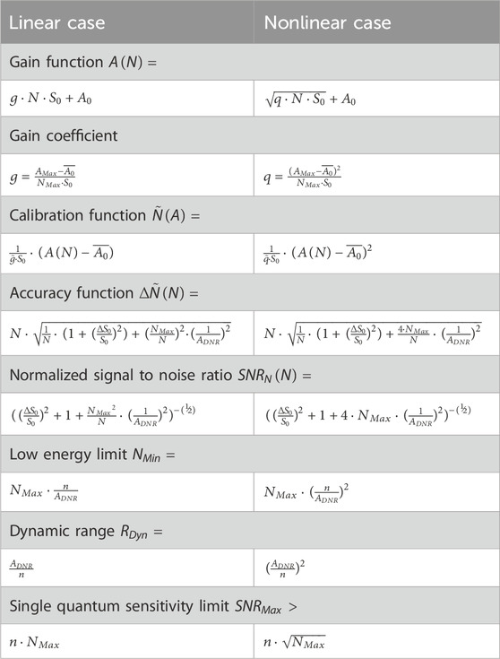
TABLE 1. Comparison of model output for relevant performance parameters of the linear and nonlinear gain function. All parameters can be expressed as algebraic expressions.
In comparison, it is obvious that, for common values of
For
The better low signal performance is countered by an accuracy worse compared to the linear gain function at higher stimuli. Figure 1A shows the comparison of the accuracy functions for a maximum number
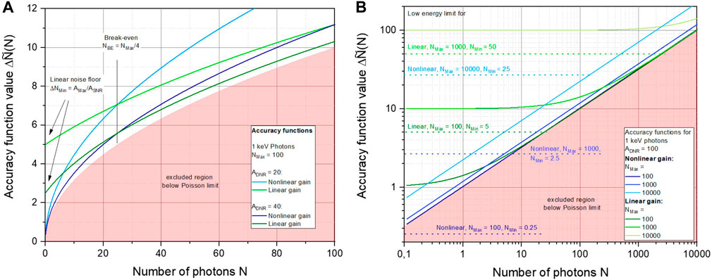
FIGURE 1. Accuracy functions for linear and nonlinear gain functions, for
The behavior scales accordingly for higher values of
Here, it turns out that the
2.3 Discussion
Using the model system as an example, it has been motivated that using a detector with a nonlinear gain function as described above has advantages over a linear approach when used within the context of photon counting applications. For low stimuli, the uncertainty on the retrieved photon number converges to zero for the nonlinear gain while the linear gain reaches a finite noise floor level, which is due to the different scaling of the amplifier noise contributions. Main advantage of the nonlinear gain is a substantially increased dynamic range and improved low signal detection limit, as can be taken from the left plot in Figure 1.
The advantage of the linear gain approach, in contrast, is the higher accuracy for the largest part of the input stimulus range. In addition, it should not be ignored, that a detector system implementing a nonlinear gain also faces some practical challenges. The idealized square root behavior is in practice difficult to implement. Practical implementations therefore use approximations of the ideal behavior. In addition, the optimized behavior is valid only for a single target energy and intensity. When these values change, deviations from the ideal behavior are to be expected. Finally, the calibration of such a detector can be a cumbersome task, given that imaging detectors for photon science target a large sensitive region with many channels, and needs to cover the complete dynamic range.
But if a large dynamic range is requested and both low and high intensity features are to be acquired simultaneously, and the higher inaccuracy for larger signals can be tolerated, a nonlinear gain is the better solution. It is an extremely useful tool for the exploration of large dynamic ranges.
3 Detectors for photon science applications
The ideal gain function for applications limited by the counting error follows a square-root behavior. To implement or mimic this behavior, several approaches are commonly applied in state-of-the-art photon science instrumentation.
At the time of writing, standard pad or pixel detectors based on PIN diodes for conversion of the X-ray photons to signal charge are widely used. This type of detector is technologically simple and easy to manufacture with high yield. When applied in large scale systems, integration is done using a hybrid pixel approach, in which front-end ICs providing one preamplifier channel per pixel are bump-bonded to the sensors, connecting preamplifier channel to its sensor pixel with solder bumps.
In this detector architecture, the task of applying the nonlinear gain is transferred to the front-end electronics, especially the preamplifier. Different approaches exist for implementing or approximating the requested shape of the gain function. The multilinear approach approximates the optimum nonlinear gain curve by a combination of multiple linear gains. One possibility to implement multilinearity is to having several (typically three) preamplifier channels per pixel operating in parallel and each having a different gain—one for low, one for medium and one for high intensities [1]. Depending on the actual stimulus, the information of the channel with the gain fitting the stimulus requirement in the best way is selected for data analysis.
A similar approximation can also be made using one single preamplifier per channel only, if the preamplifier can adapt automatically to the signal. Integrated, pixel-individual control electronics adjusts the preamplifier gain dynamically as a function of the signal level [2] by selecting one of three different gain values. The internal control logic monitors the output signal and switches the gain to the next higher value as soon as the amplitude exceed a certain threshold. In these and similar approaches, the design of the preamplifier determines the gain(s), and the shape of the effective gain function. The lowest gain is selected to meet the requirement on the upper limit of the dynamic range, while the highest gain defines the lower dynamic range limit.
The problem with Pad detectors is that their pixel capacitance is directly coupled to the pixel area, which, in combination with the high preamplifier bandwidth required for fast readout, results in relatively high noise figures, effectively limiting their low energy performance. This problem can be mitigated if the detector itself provides for a certain level of amplification, like for instance by using avalanche multiplication. Classical APDs however, suffer from homogeneity issues. The Monolithic Array of Reach-THrough APD (MARTHA) structure, however, uses avalanche multiplication for pushing the low energy dynamic range limit while avoiding the weak points of the classical approach.
3.1 MARTHA devices
MARTHA devices are based on the concept of Avalanche PhotoDiodes (APDs). APDs provide inherent localized amplification of the signal charge within the sensor, and the amplification is achieved by avalanche multiplication of the primary signal charge itself.
At the time of writing, APDs are applied in a large variety of contexts, but many more potential applications could benefit from their use. The main issue is here, that APD arrays show bad position resolution and homogeneity of sensitivity over larger areas, especially if benchmarked against what is possible for simple photo diode arrays. Consequently, APDs play a comparably minor role. Only small formats of 16 up to 64 pixels are commercially available, and the smallest dead space gaps between pixels are in the range of 40 µm [3]. Institutional R&D is ongoing for several years to close the gap to the photo diode arrays.
For the fabrication of larger APD pixel or strip arrays one has to overcome two critical obstacles. The first problem concerns the homogeneity of the avalanche gain. The ionization rates in the avalanche process depend on the electric field strength, which by itself is determined by the actual doping profile in the implants defining the potential in the multiplication region. Consequently, any fluctuation in the doping process directly affects the magnitude of the electric field. Fluctuations in implant energies results in depth variations of the implants, affecting size and position of the multiplication region, and fluctuations in the implanted dose will directly modify the overall space charge. Both effects have an exponential impact on the ionization rate, and thus the gain. These gain fluctuations need to be minimized by careful technological processing using highly specialized, well controlled and monitored processes for all relevant implantations. The effect of the yet remaining gain variations can be mitigated by operating the APD arrays at a comparably low gain. In general, gain values of 20 and below are recommended to keep the effect of gain fluctuations in a manageable range. This is a common approach, for which the R&D activities are summarized under the name Low Gain Avalanche Diodes (LGAD) development—see, for example, references [4–6].
The second problem is the early breakdown at the edges of the segmented n + diodes defining the pixel electrodes. This is caused by the elevated field strength at convexly curved doping shapes as can be found at the edges of the anode implants. To avoid the breakdown, implanted guard ring structures are commonly provided, which rigorously suppress avalanche processes at the edges of the implants. The downside is that these arrays are blind in the inter-pixel gap regions.
Concepts to suppress edge breakdown while maintaining high detection efficiency in the gap region are currently in the focus of research and development [7–10]. The Inverse LGAD (iLGAD) [7, 8] is the most fundamental approach to achieve a homogeneous lateral electric field distribution. It uses a segmented p + cathode on a p type substrate as pixel/strip read out structure. One global non-structured n + anode and p type multiplication region on the opposite side of the substrate covers the entire sensor array. The pn-junction formed by the anode and the multiplication region, however, must not touch the cutting edge, requiring more expensive double sided processing, which is even more challenging in case thinned substrates are used.
If operated as X-ray detector, photons have to enter on the non-structured n-side. If a photon is absorbed in the multiplication region, the photon generated charge experiences different amplification, depending on the depth at which they are absorbed. Although there are successful attempts to mitigate this effect [8] it still compromises the detection efficiency especially for low energy X-rays.
Another approach is to replace the implanted standard inter-pixel guard structure by a trench isolation [9]. The blind inter-pixel region can be drastically but not completely reduced to a level sufficient for particle detection. For precise energy measurements or photon counting, a homogeneous response is required.
In the Deep LGAD concept [10], the p-avalanche multiplication structure is implanted before the growth of a thick, high resistive n-type epitaxial layer, which separates avalanche multiplication from n + pixel implants located on top of the epitaxial layer. Reported simulation results show a very good edge breakdown suppression and a fairly homogeneous response behavior. Problematic with this approach is that the pn-junction between epitaxial layer and p-type bulk conceptually extends to the cutting edge of the sensor, leading to significant leakage current generation.
The MARTHA concept discussed here offers an alternative way to completely suppress edge breakdown while providing a fairly uniform signal response also in the inter-pixel gaps.
3.1.1 MARTHA concept
Figure 2 shows a cross section through two neighboring pixels of the proposed MARTHA structure. For any photon detector, optimum quantum efficiency can only be achieved without any obstacles for the incident photons. For this purpose, a Reach Through APD [11] is an ideal solution. It operates at full depletion and provides a homogeneous photon entrance window with 100% fill factor on the backside. The bulk acts as drift region. If the bulk is p-doped, the structures can be manufactured using single sided processing only, with guard structures only on the n-side.
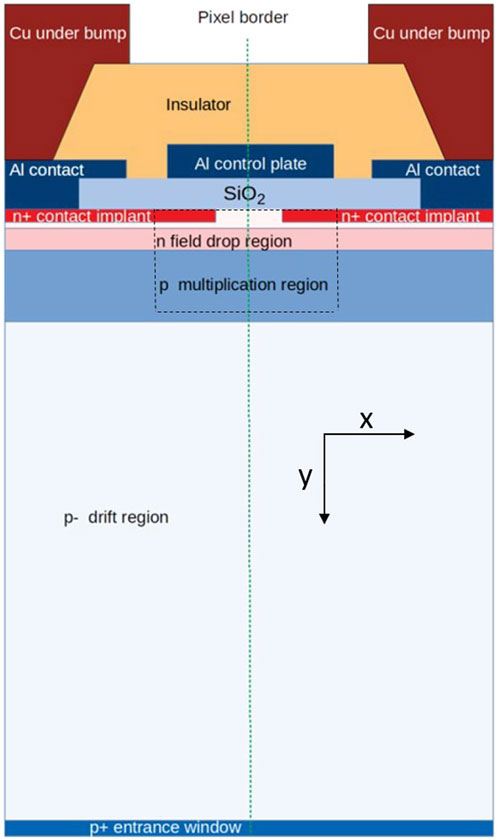
FIGURE 2. Cross section through two neighboring n + doped MARTHA pixels. Shown is the region between the two pixel centers. Radiation enters from the bottom side, and the aluminum contacts on the left and the right serve as contact points for the preamplifier electronics. The distance between the pixel centers is 50 µm. Distances are not to scale. The x and y coordinates indicate the directions relevant for Figure 4.
The pixel electrodes are formed by conventional n + anode implants. An aluminum control grid over the complete array provides flexibility in controlling the SiO2/Si interface potential in the inter pixel gap regions. This additional electrode can later be replaced by a proper surface implantation in a future implementation. Key features of the MARTHA structure are the global multiplication region (MR) and the field drop region (FDR), which is located above the MR. The MR is defined by a p-type high energy (HE) implant in a depth of several microns from the surface, the FDR by a relatively deep-n implant below the anode implants. Both implants are global and unstructured. In this way, MR and pixel implants are vertically separated in a similar way as in the Deep LGAD concept mentioned above, but the MARTHA approach has the advantage that the required doping profiles can be confined to the pixel region.
If the structure is fully depleted, the MR extends between the MR HE implant and the FDR. The FDR is important for the mitigation of the edge breakdown. Its main effect is to suppress the aforementioned peaks in the field strength. Its effect can be deduced from equivalence between the depleted implant dose and the field strength, which can be concluded from the Poisson equation. Accordingly, the absolute maximum electric field at a pn-junction is
with
where
where
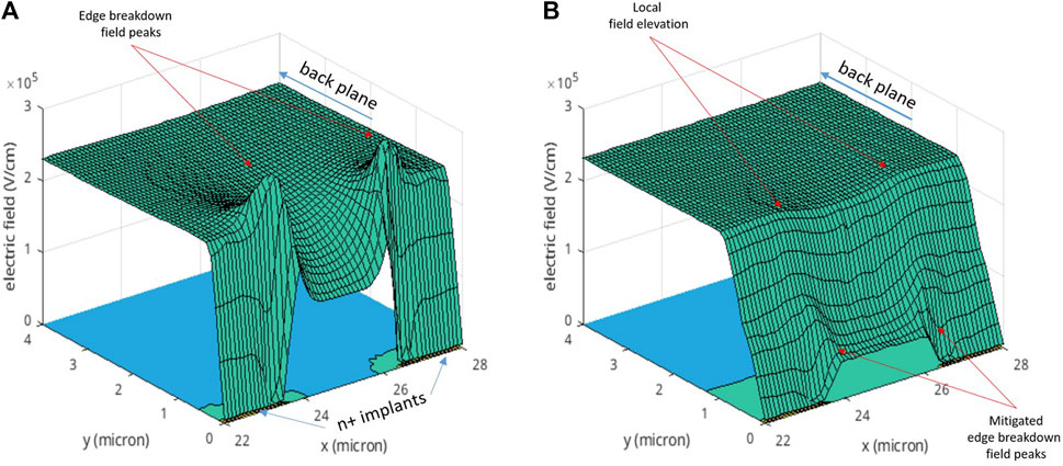
FIGURE 3. Zoom into simulation of inter pixel electric field distributions (absolute values), without (A) and with (B) field drop layer (FDR). The x and y coordinates correspond to the lateral surface coordinate and the depth in the wafer as indicated in Figure 2. The inter-pixel gap is 3 µm wide. Without FDR, the electric field peaks are prominent. A structure with FDR, in contrast, shows substantially smaller peaks, which are still visible, but suppressed to a large extend and well below the critical value for avalanche generation.
This loss can, however, be compensated if the depth of the multiplication region is increased, to that the gross charge amplification remains the same. For this purpose, the aforementioned HE implant is used to create a wide, vertically extended MR below the newly introduced deep n-doped FDR.
3.1.2 Simulation results
The simulation refers to two neighboring half strips including the gap in between. Each half strip extends over 50 µm. Taking into account the applied symmetric left/right Neumann boundary conditions the simulation domain corresponds to a strip detector array with 100 µm pitch. For this simulation, the gap between the pixels was 3 µm wide. When investigating the region below the pixel implants, the MR, between the MR implant and the FDR, shows a parallel-plate capacitor like electric field distribution. Reason for this is the very low doping concentration between FDR and the high-energy MR implant, where almost no space charge is integrated.
Figure 4 shows vertical cross sections of doping profiles through pixel and gap regions (left image) and the resulting electric fields (right image) of the upper part of a 450 µm thick sensor, determining the various regions of a MARTHA structure. The doping profile of the HE implant used in the TCAD simulations was measured by Secondary Ion Mass Spectroscopy (SIMS) on structures from a wafer from the prototyping production.
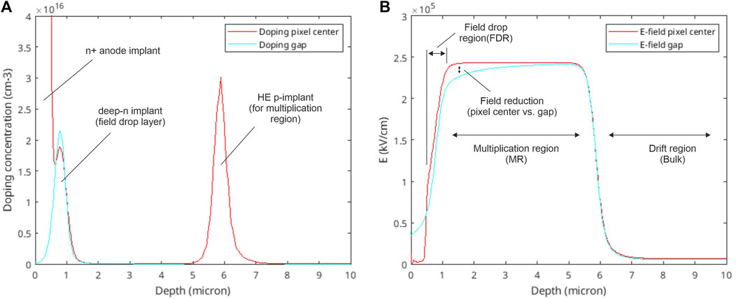
FIGURE 4. Vertical doping profiles (A) and resulting absolute electric fields (B) in the various vertical zones. Two different cuts, one through the pixel center and one through the inter-pixel gap are shown. Clearly visible are the near-homogeneous field in the multiplication region especially in the pixel center. The field reduction in the inter-pixel gap is caused by the more negative surface potential, but its influence is mitigated by compensating effects.
In the inter-pixel region, however, a reduction of the electric field in the MR can be observed, in the order of around some 10%, which increases with decreasing depth. This field reduction is a result of the potential at the SiO2/Si interface, which must be more negative than the anode potentials in order to provide sufficient inter strip/pixel isolation. But this electric field does not result in a reduced avalanche generation in the gap region. Figure 5 shows the result of a charge generation scan simulation over the horizontal coordinate, which was done to evaluate the sensor response in the gap region. The simulation demonstrates that almost no charge loss in the gap region occurs. About 800 electrons were injected in a depth of 448 µm below the anode contact. In this simulation, the structure works with a gain of about 14 in the preset bias conditions.
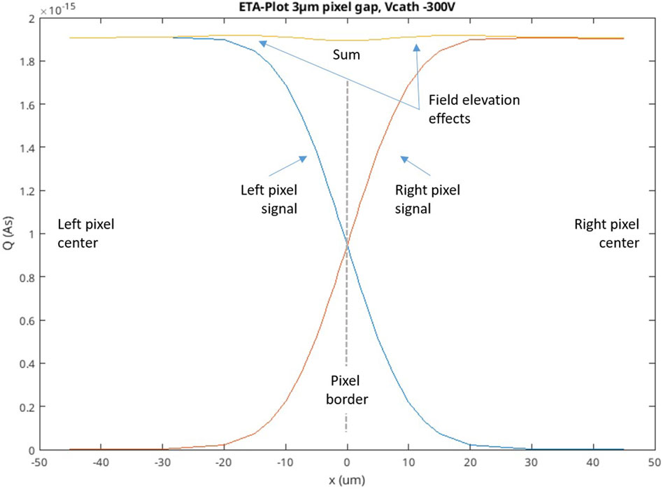
FIGURE 5. Simulation of signal charge response, to test charges generated at different horizontal positions x in a depth of 448 µm. The signal level detected by the left anode is shown in blue, and the right anode signal is shown red. The sum of the signals is indicated by the yellow line. The simulation indicates that the structure does not have insensitive regions in the inter-pixel region. Overall simulated signal injection was about 800 electrons, and the structure operates at a gain of about 14.
Two mechanisms help to compensate the effect of the reduced electric field. At first, the negative gap potential creates an additional drift field, diverting charge generated below the gap region towards the n + doped anodes, where they are exposed to the nominal field strength and experience the specified amplification. In addition, the simulations suggest that a 2-D effect, already faintly visible in Figure 3B, also helps to compensate the effect of the field drop. A local field elevation appears on each side of the gap, which is laterally displaced from the n + pixel edge by a few µm towards the pixel center. Although the field elevation is of the order of about only few percent, its magnitude is sufficient to affect the amplification. Accordingly, the simulated response curves shown in Figure 5 indicate a region with slightly elevated response compared to the anode centers, at the order of up to 1%, in the regions left and right of the pixel borders, showing a maximum at about +/- 15 µm.
Similar simulations were made to study timing behavior and signal formation inside a MARTHA structure. A test charge of 0.134 fC was generated close to the backside in a depth of 448 µm beneath the left anode. Figure 6 shows the time dependence of signal currents and their integrals, the amplified signal charge. The plot compares the MARTHA pixel structure with standard pixel without avalanche multiplication. The simulation reveals that the detection of the full signal lasts longer in the MARTHA scenario, as the holes generated in the multiplication layer have to drift a significant distance towards the cathode until the full signal is established. This is a feature common for all types of APDs.
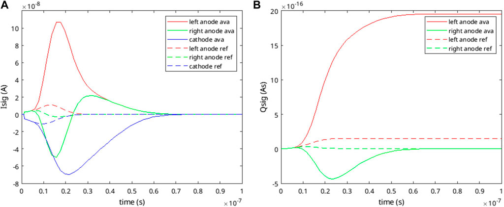
FIGURE 6. Evolution of signal currents (A) and signal charge (B) in a MARTHA structure after generation of a test charge of 0.134 fC at the backside of the sensor beneath the left anode. Generation depth is 448 µm. Solid lines represent the amplified currents and charges. For comparison, the same simulation was performed on a standard PIN diode structure without avalanche generation (dashed lines).
Accordingly, the induction current on the right anode is more pronounced compared to the situation at the standard diode. This is because in the standard diode the current is induced by drifting electrons according to the weighting field only, while for the MARTHA structure the right anode additionally ‘sees’ the induction current of generated holes drifting in the opposite direction. It gradually disappears the more the holes approach the cathode. Eventually the right anode net signal is zero in both cases. In summary, the signal rise time is comparably fast, but the simulations indicate that the detection of the full signal lasts longer compared to a diode.
Conceptually, the MARTHA structures are suitable for both X-ray and particle detection, but some optimization with respect to the application is required. Common to both applications is the need for high detection efficiency. MARTHA structures fulfill this requirement, as they are backside illuminated structures with high fill factor, and the FDR eliminates the need for insensitive guard ring structures. Applying suitable antireflective coating (ARC) on the backside entrance window to match the QE to the application requirements allows for customization of the MARTHA structures also for use with optical wavelengths.
Using MARTHA structures for the X-ray wavelength range requires low noise operation for good energy resolution and precise photon counting, especially when low photon energies are used. In addition, an adaption of the substrate thickness is required. To detect higher X-ray energies with acceptable QE, substrates with a thickness at the order of 450 µm or higher are required. These substrates are compatible with the HLL standard entrance window technology, which provides for excellent quantum efficiency up to an X-ray energy of 12 keV [14].
For applications in particle tracking, in contrast, thinned SOI substrates are a suitable option as an effective way to reduce the radiation length. Here, substrates with a thickness of 50 µm or less are feasible.
The devices in the ongoing prototyping production were optimized for X-ray detection. The structures are integrated on highly resistive p-type float-zone wafers with standard thickness of 450 µm. Reach through diodes need to be operated in full depletion. The high-energy implant defining the MR is applied to the area inside the pixel/strip array only, and the implant is lithographically masked at the sensor edges. This simplifies the design by avoiding interference with the guard ring structure on the n-side.
Silicon wafers with this bulk thickness are suitable for X-rays in a medium energy range up to 12 keV. Using a wide MR and a thick wafer leads to a relatively high operation voltage. Four our chosen parameters, depletion of the high field region and the thick wafer needs about −140 V and −120 V, respectively. Adding a moderate over-depletion voltage results in an operation voltage of about −300 V. On the other hand, the electric field depends only weakly on the backside voltage. Therefore, if the sensor is operating with low gain only modest gain changes are to be expected, in case the bias voltage fluctuates or the bulk doping shows variations.
For soft x-rays below 1 keV, thin entrance window implants with minimum dead layer are required. These thin entrance windows suppress the recombination of signal charge in the undepleted part of the heavily p-doped cathode, so quantum efficiency and spectral performance improve. The respective technology steps are compatible to the MARTHA process.
To summarize, MARTHA structures have the potential to overcome the traditional limitations of APD arrays. In photon science applications, their gain properties help to push the low energy limit of the dynamic range. Concerning the high-energy limit of the dynamic range, gain-reducing effects observed at higher intensities [15] are subject of ongoing investigations. These could also help to accommodate the requirements from the application.
In case minor modifications concerning biasing are adopted, the devices can work together with most classical front-end solutions forming a hybrid pixel assembly. If combined with an advanced multilinear frontend, they can service the complete dynamic range as requested by state-of-the-art photon science experiments and provide for an attractive alternative to traditional pad and pixel detectors especially for detecting low energy X-rays.
Based on the abovementioned TCAD simulations, a generic MARTHA technology plan was conceived and optimized. A first prototyping production was finished recently at the MPG HLL; the prototype detector structures await qualification measurements.
3.2 pnCCDs for high dynamic range
Pad or Pixel detectors in a hybrid pixel detector are an appropriate solution if for instance extremely high framerates are required, as they provide for the option of full parallel readout of the complete detector. Disadvantages are high complexity of integration, high power consumption, comparably large volumes and the need for advanced mechanical and thermal interfaces, in combination with a low energy threshold, which is comparably high. In addition, the hybrid pixel approach demands similar pixel pitch on sensor and front-end electronics. This brings about limitations in terms of scalability of pixels sizes. In case resources are less abundant and the experiment requires a more compact sensor system, a lower system noise or smaller pixels are requested, and lower framerates can be tolerated, pnCCDs can be an attractive alternative.
3.2.1 pnCCD structure
The pnCCDs have originally been developed as sensors for imaging X-ray spectroscopy for the X-ray satellite mission XMM-Newton [16, 17] and since then found application in a wide variety of experiments in X-ray astrophysics as well as high luminosity X-ray sources [18–21].
Figure 7 illustrates the structure of a pnCCD. The pnCCD concept is based on sidewards depletion, and the devices are manufactured in a double sided process. The backside provides a homogeneous, unobstructed, ultra-thin entrance window for radiation. Customization of the entrance window, e.g., by deposition of anti-reflective coatings or light blocking filters is possible if required by the application. On the frontside, a high-energy (HE) n implant several micrometers below the surface defines the potential minimum for electrons which forms the transfer channel. In transfer direction, p + implants connected to form a three-phase register structure define the CCD pixels. The pixel size can be scaled between 36 µm up to 150 µm to match the experimental requirements.
FIGURE 7. Structure of a pnCCD. A pnCCD is built by utilizing p + implants forming the different registers and a deep-n implant forming the transfer channel in several micrometers of depth. By clocking the registers, the charge is transferred to the readout nodes. The transfer direction, indicated by the arrows, is perpendicular to the p + register implants (shown in red).
Perpendicular to the transfer direction, additional deep implants, the n-type channel guide and the p type channel stop, define the pixel structure. These implants create potential barriers between the pixel columns, confining the signal charge to the pixel. Utilizing a three phase clocking scheme, the charge is transferred from pixel to pixel, and finally handed over to the n + readout anode. The readout node is connected to the gate of the FirstFET, a low noise n-channel jFET with an equivalent gate capacitance of 50–100 fF. It is typically read out in a source follower configuration. With readout rates of 4 µs per line, an input capacitance this low provides for noise figures of a few electrons ENC.
A pixel of the pnCCD stores the signal charge below one of its registers inside a potential pocket in the n-type HE implant, which also serves as transfer channel. The register structure confines the signal charge transversally, and lateral confinement is given by the deep-n channel guide and deep-p channel stop implants. The depth of this potential well defines the pixels CHC. A state-of-the-art pnCCD, with a pixel size of 75 μm2, can store a few 100 ke-per pixel in standard operating conditions [22].
Although this is sufficient for most spectroscopic applications, the situation is different for ultra-luminous sources, as used for scattering experiments. Here, certain regions on the sensor are illuminated with high intensity, several thousand up to several hundred thousand photons and more can be collected within a single pixel. The amount of signal charge thus generated exceeds the charge-handling capacity of a pnCCD in standard operating conditions, leading to an overflow of the charge into neighboring pixels, an effect observable as blooming or smearing in the recorded images. Increasing the pixel CHC of a pnCCD is, however, possible by optimizing the operating conditions.
The standard operating conditions create the potential well defining the pixel in a depth of several micrometer below the surface, with the depth mainly being defined by the deep-n transfer channel implant. A more negative backside voltage, however, lowers the positive potential formed by this implant. Below a certain voltage level, the vertical potential barrier is overcome and the charge in the transfer channel is pushed closer to the surface, into a secondary potential well formed by the channel guide implants. In effect, this increases the capacitance of the pixel and allows storing more charge within it. A pnCCD with 75 μm2 pixels operated in this high dynamic range mode exhibits a pixel CHC to up to 2 × 10⁶ e− and more, without exhibiting bleeding effects, which is sufficient for the use in photon science experiments [22].
3.2.2 pnCCD readout
Conceptually, pnCCDs are charge integrating devices, which are read out on demand. The image is generated by integrating signal charge for a defined integration time. Afterwards, the charge is read out by transferring it to the readout nodes.
A fundamental limitation of CCDs is that the charge needs to be transferred serially to the readout anode for every pixel, which puts up an intrinsic limit for the degree of readout parallelization. Unlike many conventional CCDs, pnCCDs provide one readout node per sensor column, and the front-end electronics processes the information of all sensor columns in parallel, so that no lateral transfer is required. This is referred to as full column-parallel readout. By suitable segmentation and matching interconnection of the register contacts, a split-frame readout can be realized. For such a device, readout anodes and first FETs are present on both edges of the CCD, to which the signal charge from the adjacent half of the sensor pixels is transferred. In this way, a two-fold column-parallel readout can be implemented, effectively reducing the readout time by a factor of two. A higher degree of parallelization cannot be realized on a monolithic pnCCD device. Further topological modifications are possible for pnCCDs, which, however, do not influence the readout speed. A frame store area [23], for instance, is primarily introduced to suppress so-called out-of-time events (OOTs), which are events registered by the CCD during the readout phase of the image. Due to the frame store area, OOTs can be suppressed to a large extend at the cost of substantially larger device area and additional transfer time, which slows down the readout. Therefore, a frame store is mainly useful for improving the image quality under continuous beam conditions with low to medium beam intensity.
Once the charge is transferred to the readout anode, it causes a voltage change at the gate of the FirstFET. In the classical JFET configuration, the FirstFET of a pnCCD can only be operated in source follower configuration for topological reasons. Here, constant current bias is provided to each FirstFET, usually by a current source integrated in the associated front-end channel. In first order approximation, the additional charge on the FirstFET gate increases the gate voltage by about:
This source voltage step is acquired by comparing the source voltage level of the FirstFET. The baseline level before the transfer, and the signal level after the transfer are acquired and subtracted from each other. This technique is commonly referred to as correlated double sampling (CDS), and requires a time-variant preamplifier/shaper circuit. CDS provides superior 1/f noise suppression.
Several readout ASICs are available that are capable to process the signal of the FirstFETs via CDS, using either multi-correlated double sampling or a trapezoidal weighting function for filtering [24, 25]. Readout rates down to 2 µs per column can be realized with excellent noise properties and fano-limited energy resolution for X-ray spectroscopy.
This excellent performance is also a consequence of the nature of the pnCCD being a sidewards depleted device. The conceptually small capacitance of the FirstFET Gate/readout anode increase the signal voltage step, directly affecting the signal to noise ratio.
The FirstFET gate/readout anode contacts can be reset to a defined voltage level using the so-called ResetFET It can be biased statically, causing slow discharge from the readout anode to the drain of the reset FET, keeping the readout anode voltage in a dynamic equilibrium depending on the reset FET bias and the amount of incoming charge. This mode works best for low to medium occupancy, e.g., in spectroscopic applications. Alternatively, the reset FET can be operated in pulsed mode, resetting the readout anode contacts after a fixed number of readout cycles. This mode is useful to restore defined biasing conditions in operation modes with large quantities of signal charge. In the most extreme cases, the readout anodes have to be reset after each readout cycle.
Considering a CCD with
In this way, a state-of-the-art column-parallel pnCCD can be operated at framerates of between 480 Hz and 930 Hz for a standard mode device or 460–890 Hz for a framestore device, assuming a split-frame CCD topology with a 1 k × 1 k pixel large imaging area. Accordingly, the readout of smaller sensors scales linearly with their size.
Conventional large area pnCCD systems have successfully been deployed to experiments at free electron lasers, namely, the CFEL-ASG Multi-Purpose instrument (CAMP) [19] and the Laser Applications in Material Processing (LAMP) [20] experiments at the Free-electron LASer in Hamburg (FLASH), and the Linac Coherent Light Source (LCLS), respectively. The concept for the LAMP instrument is shown in Figure 8B, a photo of one pnCCD module is shown in Figure 8A. The X-ray laser illuminates the specimen, and the various CCD detectors record the speckle. The image data is used to reconstruct the structure of the specimen [26]. The main challenge in this kind of experiment is the simultaneous observation of large and small scattering angles that typically have orders of magnitude difference in intensity. To resolve single scattered photons, a sufficiently low noise is required, while high numbers of photons demand a large charge handling capacity.
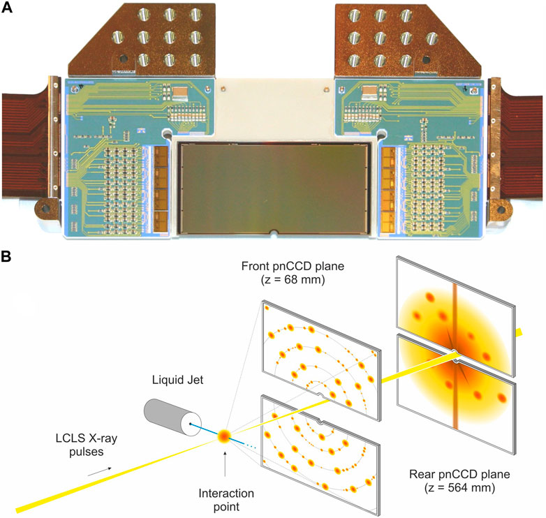
FIGURE 8. Photo of a pnCCD module as used in the CAMP and LAMP experiments (A). The structure is a standard mode, split frame pnCCD. To cover a larger solid angle, two modules can be placed close to each other with minimum dead area. The hole in the central region allows the un-scattered primary beam to pass. Setup of diffraction experiments at CAMP and LAMP using the pnCCD modules (B), using two planes of two pnCCD modules each. The setup corresponds to the one reported in [26].
3.2.3 pnCCD gain
While the register structure of a pnCCD is capable of handling several 106 e- within a single pixel, processing the charge puts up a challenge for the following readout chain. At first, the input stage of the preamplifier ASICs will face signal voltages of several volts, due to the small readout anode capacitance, so special precautions have to be taken not only in order to be able to process the signal levels correctly, but also to prevent damage to the preamplifiers. The respective ASICs need to be furnished with a HV input stage, with configurable attenuator circuitry if necessary.
What is more, the requirement to resolve single photons as well as the extremely high signals in the peaks simultaneously cannot be fulfilled by the conventional CCD readout systems applying preamplifiers with linear gain. As discussed before, multi-linear or non-linear amplification can optimize the system response for photon counting applications. The JFET used for the conventional pnCCD readout, however, is operated in a standard source follower configuration, has a linear characteristic and does not support a customized gain nonlinearity.
The nonlinear or multilinear gain could be integrated into the readout amplifier, but at the time of writing, a pnCCD compatible preamplifier solution implementing these features does not exist. Current pnCCD preamplifiers are conceived for spectroscopy and offer a number of different gain settings, but they can only be operated with one specific gain setting at a time. Depending on the gain setting, information from either high or low intensity features is therefore lost. As a workaround, scattering images from the same specimen are taken with several gain settings, and the data is combined later on in the analysis. This pragmatic workaround is, however, only suitable for specific types of application scenarios.
A customized preamplifier with the option of multilinear amplification, which would be a new development, would be useful for standard CCDs with a simple anode-based readout, but would not necessarily be the optimum solution for the pnCCD. This is because of the pnCCDs FirstFET, which is the first element in the signal amplification chain. The gain nonlinearity is most effective if it is applied as early in the signal processing as possible.
As shown in section 2, a linear gain function introduces a constant offset to the accuracy function, while the accuracy function for the nonlinear gain converges to zero for small signals. In case of a linear amplifier (e.g., the FirstFET) as primary and a nonlinear amplifier as secondary stage, the FirstFET introduces an offset to the accuracy function, and the secondary stage amplifies this offset with a gain corresponding to its level. For a nonlinear first stage followed by a linear preamplifier, however, the offset to the accuracy function is zero, and, although the linear secondary stage introduces an offset on its own, this offset is not amplified further, so that this configuration has better accuracy at low signal levels.
Implementing the gain nonlinearity into the FirstFET will therefore be superior compared to solutions based on nonlinear or multilinear preamplifiers. An approach currently being developed at the MPG HLL is the replacement of the conventional FirstFET based on a JFET with DePFET based end-of-column amplifiers for the readout of pnCCDs. Critical issue here is the transfer of the signal charge from the transfer channel of the column defined by the HE implant to the internal gate of the DEPFET serving as EOC amplifier. In this process, all charge needs to be transferred, even for very high signal levels, without compromising the image information. Once this process is complete, the device benefits from the unique capabilities of the DEPFET.
As described below, DEPFET structures allow the implementation of a customized non-linear amplification already on sensor die level. A combination of a pnCCD pixel array with an optimized pixel CHC for photon counting with high dynamic range, and a DePFET based EOC amplifier with customized nonlinear amplification is a useful detector device for x-ray scattering imaging with high dynamic range. In addition, it could also help to speed up pnCCD readout.
Although a source follower configuration for readout has some benefits, e.g., its invariance against bias voltage settings and its robustness against radiation-induced threshold voltage shifts, it also puts a limitation on the readout speed. In the source follower configuration, the load capacitance connected to the source node needs to be recharged each time the source voltage changes. This recharge process is driven by the
For photon science a large format pnCCD with a DePFET based readout node, incorporating a non-linear signal response would provide kHz readout rate and large sensitive area with maximized dynamic range. A first small format prototype combining a pnCCD with a DePFET based first amplifier has recently been manufactured. The test system is under construction.
3.3 DEPFETs for photon science application
As mentioned above, DEPFET [27] devices provide for a different approach to create required nonlinear characteristics, not in the preamplifiers, but in the sensor itself. This is the principle of in-sensor signal compression. Although a more sophisticated sensor is required, the design of the front-end amplifiers can be simpler and less customization is required. DEPFET devices can be used in multiple ways and in a variety of contexts. As mentioned, they can be combined with a pnCCD pixel structure replacing the traditional JFET based FirstFET, adding gain customization and higher readout speed.
They can, however, also be used as building block of an active pixel sensor (APS). The advantage here is a significantly higher framerate, as a much higher degree of readout parallelization is achieved in this way. One example is the so-called EDET sensor using a 4-fold multiparallel readout to achieve a framerate of 80 kHz for a 1 MPixel array. The extreme case is the full parallel readout using the DEPFET APS as basic cell of a hybrid pixel detector, which has been realized for the so-called DSSC (DEPFET Sensor with Signal Compression [34]).
3.3.1 The DEPFET detector/amplifier structure
The combined detector amplifier structure DEPFET [27] (Depleted P-channel FET) has found application in a variety of projects, ranging from high-energy physics [28, 29], extraterrestrial physics [30, 31], planetology [32, 33], and photon science [34]. A DEPFET structure essentially consists of a PMOS transistor integrated on the surface of a fully depleted, n-type silicon bulk. By means of sidewards depletion, the potential minimum for electrons created in this way is shifted towards the surface on which the PMOS structure is located (see Figure 9). Using an additional n implant, the potential minimum is further enforced and confined to the region just below the PMOS gate. Bulk-generated electrons will follow the drift field created by the sidewards depletion, and will be collected in the potential minimum beneath the PMOS gate. Here, their presence modulates the PMOS current in the very same way as charge on the external gate. Therefore, the potential minimum is referred to as internal gate. The figure of merit for the internal gate is the so-called charge transconductance, or
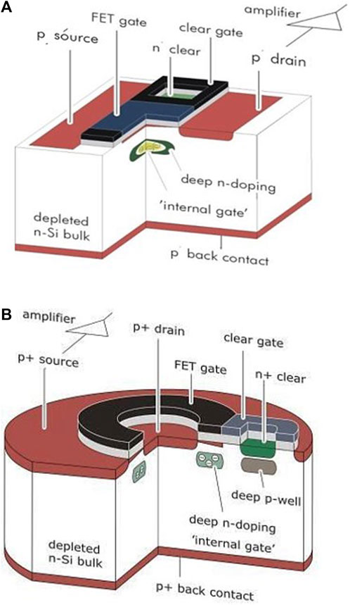
FIGURE 9. Cross-cuts through simple DEPFET devices with linear (A) and circular (B) transistor geometry. Basic structure is a PMOS transistor. A space-charge region created by a deep-n implant below the PMOS collects the bulk-generated signal charge. The charge in this “internal gate” controls the PMOS current. The charge can be removed using an additional NMOS, the so-called ClearFET. Both variants, circular and linear, have been used for experiments, but the linear variant has advantages in terms of scalability and high integration density.
The DEPFETs nature as sidewards depleted device brings about additional benefits. DEPFETs have an extremely low internal gate capacitance of only few fF, and therefore exhibit intrinsically high signal to noise ratios. They have in common with pnCCDs that in most cases they are illuminated from the backside, which allows for 100% fill factor and provides a certain degree of self-shielding, especially against low-energy X-rays. In addition, the sensors can be furnished with an entrance window configuration optimized for the respective application, e.g., antireflective coating for QE optimization for use in the optical wavelength, or thin entrance window implants for good spectral performance even for the lowest X-ray energies.
3.3.2 DEPFET clear
Conceptually, the DEPFET is a charge integrating type of device. Without external influence, the internal gate will collect all bulk-generated electrons, which continuously lower its potential. To clear the internal gate of the collected charge and to reset the DEPFET structure to a defined state, the clearFET, a dedicated NMOS structure merged with the PMOS, is used. The clearFET uses a separate cleargate contact as gate and an implanted n + contact, the clear contact, as drain, while the internal gate acts as source. In normal biasing conditions (Clear OFF state), the clear contact is shielded from the bulk and the internal gate by the barrier created by the cleargate and an additional deep-p shielding implant. When the internal gate keeps collecting charge, its potential will eventually reach the potential of the barrier towards the clear. This point defines the CHC of the DEPFET, as from now on, excess charge will start leaking to the clear, and the potential of the internal gate will remain constant.
By applying a positive voltage to the cleargate, the potential barrier between internal gate and clear is lowered, and by setting the clear to a positive voltage as well, electrons from the internal gate are extracted by the clear. If clear and cleargate potentials are set appropriately (Clear ON state), all collected charge is removed from the internal gate.
During operation, clear pulses with a fixed frequency are applied to the pixels. In the phase between the clear pulses, the DEPFETs internal gate will integrate and store bulk-generated charge. Each clear pulse will completely empty the internal gate, and the height of the step produced by the clear pulse is used as a measure for the total amount of charge collected in the internal gate during the charge integration phase. This is done by comparing the signal levels of the DEPFET in the (partially) filled state before the clear and the empty state after the clear. The signal step is evaluated using CDS with dedicated preamplifier/shaper ASICs. Sometimes, e.g., in cases requiring extremely short readout times, no individual baseline, only one pixel-individual reference value is measured for the complete acquisition cycle. Thus, the same value is subtracted from all full state signal levels, compromising the noise figure in favor of the readout speed.
An important point to mention is that the DEPFET can be used as an integrating type of detector using readout on demand. Its internal gate can store charge regardless from the presence of a transistor current. This allows the detector pixel to reside in a low power biasing state, while all the pixels are still sensitive.
3.3.3 DEPFET readout
As mentioned before, the charge in the DEPFETs internal gate influences the channel conductivity in the PMOS channel. To evaluate the channel conductivity, two common methods are in use. Like the FirstFET of a pnCCD it can be operated as a source follower. Changes in the charge collected in the internal gate will then be converted into a voltage step at the source of the DEPFET, which, in first order approximation, is
as the external gate tries to keep the source voltage at the old level. To circumvent the intrinsic limitations of the source follower, an increasing number of applications use the so-called drain readout, where the DEPFET is biased with constant potentials on drain and source, and changes in the internal gate charge are converted to a current step, which is evaluated by means of a Trans-Impedance Amplifier (TIA):
Main advantage of this approach is the higher speed. For the source follower the source node has to be recharged to its new potential during signal formation. In this process, the capacitance of the source in combination with the
3.3.4 DEPFET matrix operation
Due to their nature as sidewards depleted devices, DEPFETs can be utilized as sensitive elements for pixels in a variety of detector configurations, covering a wide range of pixel sizes from the mm scale, e.g., if surrounded by driftrings, down to few tens of µm if highly dense, coupled designs are chosen. They also provide for a huge variety of options for in-pixel functionality, like electronic shutters, multiple storages, repetitive sampling and many more [35, 36]. In the simplest configuration, however, the sensor surface is subdivided in a rectangular array of pixels, each of which is furnished with a DEPFET as central detector/amplifier element.
Conceptually, the DEPFET provides for a high degree of flexibility concerning pixel interconnection and readout, as all relevant terminals are individually accessible. Arbitrary patterns of pixels could be flexibly addressed and read out on demand, with a readout speed adapted to the respective signal. In practice, however, only two different readout configurations have found their way into application. The first approach is the fully parallel readout, where all pixels are connected to the same control- and bias traces, and all readout terminals are connected to their own individual readout electronics channel. This approach has been implemented for DEPFETs for the DSSC, and also for high-speed spectroscopy. Fully parallel readout offers highest framerate and readout speed capabilities, especially if combined with drain readout. This approach is, however, also most challenging for large area matrices due to, e.g., the required high integration density of the readout electronics, fast timing requirements, and high demands on the driver electronics for the control terminals.
The second approach is the so-called n-fold parallel readout, where different subsets of pixels share their readout electronics, and only one subset of pixels is read out at a time. A topologically simple subdivision here, which is also the most widely used, is connecting all pixels of one, or sometimes a number of
3.3.5 DEPFETs with nonlinear amplification
It was stated above that the nonlinear characteristics needed to match the accuracy of counting error can also be achieved by modifying the response of the detector itself, rather than by dedicated front-end electronics. The DEPFET structure is an ideal platform for the implementation of such an approach due to its operation principle. The DEPFETs gain characteristics can be precisely modified using
The DEPFET translates the presence of signal charge in the internal gate into a modulation of the PMOS current. The mechanism here is that the charge carriers in the internal gate induce mirror charge in the PMOS channel, which contribute to the overall channel conductivity, in the same way as charge on the external gate creates the channel in the first place. To achieve maximum influence of charge in the internal gate, the design must minimize stray capacitance towards adjacent electrodes other than the PMOS channel. To achieve this, a weak deep-n implant creates a space charge region, which confines the signal charge in a certain depth and position right below the external gate.
Within a typical pixel environment, potential barriers from source and drain and the potential barrier to the clear surround the internal gate. The potential barrier to the clear usually defines the pixels CHC, as charge starts leaking to the clear once the internal gate becomes negative enough to allow electrons to overcome this barrier.
The idea behind the technique of
Once the threshold fill level is reached, charge will start to extend to the overflow region, which will see a much higher parasitic capacitance towards the source, so its influence on the PMOS current will be much lower. The parameters of the deep-n overflow implant, mainly dose and size, adjust both the fraction of source area the overflow will extend to and the threshold value at which the overflow will occur. In effect, these parameters determine the onset point (commonly referred to as “kink”) and the effective
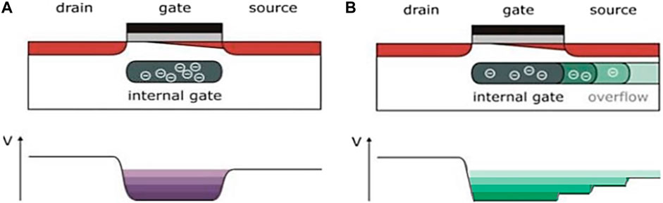
FIGURE 10. Principle of nonlinear response with a DEPFET device. Standard DEPFET Devices (A) have their internal gate underneath the external gate. Mirror charge is induced only in the PMOS gate, and stray capacitance is minimized. For a DEPFET with nonlinear response (B), dedicated overflow regions under the source are created. Above a certain fill level, signal charge starts to spread underneath the source. Here, the parasitic induction to the source is much larger, effecting a much lower gq than for the base charge. The overflow regions can be created using “graded” internal gate implantations. The superposition of multiple deep-n implants creates an internal gate extending underneath the source in several steps. This creates fill level sections with different gq each.
In this way, a DEPFET device with graded internal gate is generated, where different sections in the dynamic range show different
An example of DEPFET characteristics with nonlinear gain manufactured for the DSSC at the MPG HLL is shown in Figure 11. The DSSC uses large modules with hexagonal DEPFET pixels with circular geometry similar to Figure 9B. Gate and source concentrically surround the drain, which is located in the center of the pixel, only sparing the clear region. Accordingly, the various overflow regions extend concentrically underneath the part of the source region defined by the pson. Outside the overflow regions, the conventional p + implant in form of a concentric ring reaching out to the first drift electrode defines the source region. To fill the pixel area of 200 × 200 µm2, a drift structure with two drift rings surrounds the DEPFET readout node. The DEPFETs operate in pulsed clear operation mode, where all pixels are read in parallel with an overall maximum framerate of 5 MHz. The preamplifiers contact the sensor pixels via bump bonding.
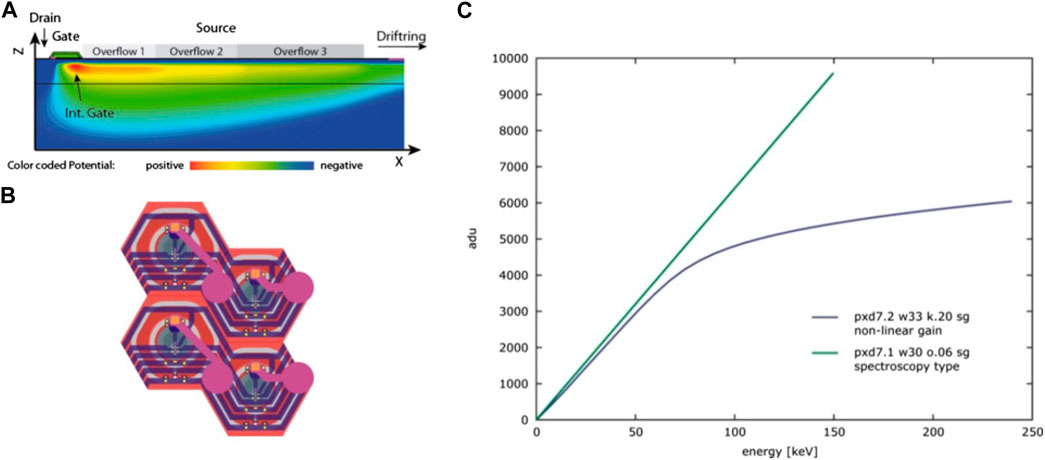
FIGURE 11. Implementation example for nonlinear characteristics. Inlay (B) shows the layout of nonlinear DEPFET pixels for DSSC in hexagonal geometry with 200 µm pixel size. Here, the graded internal gate potential is created by an overlay of three different deep-n implants. Inlay (A) shows a radial cut from the center of the pixel to its circumference. The potential distribution in the pixel area is color-coded. The three overflow regions of the internal gate are indicated by yellow to red colors, indicating the potential becoming more negative for regions closer to the pixel center. Inlay (C) shows the resulting gain curve is shown in blue. For comparison, the green curve shows the (linear) gain curve of a traditional spectroscopy grade DEPFET device.
The hexagonal approach for DSSC works well, but is of limited scalability, as far as pixel size is concerned. The smaller the pixel size, the more difficult it gets to superimpose the various deep-n implants underneath the limited source area. For smaller pixels, a different approach providing for easier scalability has been developed [39, 40]. Here, the
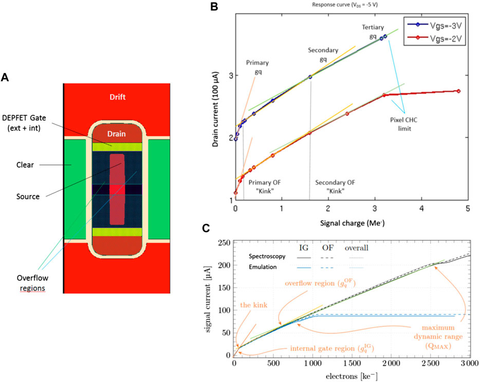
FIGURE 12. Implementation examples for nonlinear characteristics. Inlay (A) shows the pixel design for the EDET DH80 k direct electron detector for TEM imaging with 60 × 60 μm2 pixel size. Here, the graded potential was created by geometrically tailoring the p + implant for the source, which partially compensates the deep-n for the internal gate. This has a similar effect on the internal gate as the graded deep-n approach, but is technologically simpler. The layout generates the gain curves as shown in (B, C) for different operating conditions. The wedge shape on the right side of the source implant creates the second kink, or overflow (OF). Inlay (B) shows the simulated performance curves, inlay (C) the performance as measured. The upper plot shows the simulated performance curves, the lower one the performance as measured on prototype devices. The main features from the simulation can be found in the measured performance curves as well, although the secondary kink seems to be at slightly lower charge values, and the difference between secondary and tertiary gq appears to be smaller than expected. The blue curves correspond to simulated operating conditions after receiving severe radiation damage and show th expected decrease in CHC. This effect can be mitigated by annealing.
Unlike DSSC, the target application for the EDET detector is not photon counting, but intensity measurement in the focal plane of a TEM. Here, the transition of the TEM primary electrons deposits the signal charge in the detector, and the intensity is measured by counting the number of primaries. To avoid compromising the spatial resolution by multiple scattering, the detectors pixels are integrated on a thinned SOI substrate, with a substrate thickness of only 50 to 30 µm. The target application uses a primary electron energy of around 300 keV, depositing 8,000 electrons (MPV) each in the 50 µm thick substrate. To achieve sufficient contrast, a pixel should be able to store the signal charge of up to 100 primaries, which yields a pixel CHC larger than 800 × 103 electrons. It needs to be noted that for this application, the stimulus error
Due to the spatial constraints the design has to be more compact compared to the circular DSSC sensor with its isolated 200 × 200 µm2 pixels. The basic building block of the EDET sensors is a so-called couple of two pixels with linear geometry, with 60 × 60 µm2 area each. The couple partners are rotated by 180° with respect to each other. The pixels within one couple share source, clear, cleargate and gate contact, so the pixels have to be read out in parallel. Each couple partner is read out via its individual drain contact. The final matrix layout places couples next to each other in a row, in such a way that they share the common clear areas. Negatively biased p + regions, the so-called drift electrodes, separate the different rows of couples and act as a focusing implant for the bulk generated charge similar to the driftrings for DSSC.
The main improvement compared to the DSSC technology is that the geometry of the source electrode generates the nonlinear gain. As for DSSC, two implants define the source area, the pson and the p+. But as the p + compensates the deep-n in large parts, and the pson does not, the overflow region extends only underneath the pson. Thus, the layout of the p + implant modifies both size and potential of the overflow region underneath the pson. By modifying the details of the p + shape, e.g., adding a wedge or curvature, the effective
The CHC of the pixels has two limitations. As soon as the overflow region of a pixel is filled to a level at which the potential of the internal gate becomes more negative than the potential barrier to the neighboring couple partner, charge will start to spill over to the internal gate of the couple partner (primary CHC). The couple partner will then start to see the charge injected into its neighbor. This “couple spillover” will continue as long as the pixels have different fill levels. Once the couple partner is filled up as well, the couple will resume being filled up until the clear barrier is overcome and charge loss occurs (secondary CHC). The layout of a pixel couple is what is show in Figure 12, alongside with simulated and measured performance curves. An initial CHC of 3 × 10⁶ electrons has been verified. CHC will suffer in the long run under irradiation mainly due to cleargate voltage shifts, but this effect can be mitigated by annealing. In addition, radiation hard oxides for the DEPFET have been successfully prototyped.
For the intended application [41], direct bump-bonding of the front end electronics on the sensitive area is not the preferred solution, as the materials of the frond end ICs and the bumps cause backscattering, which spoils the imaging performance. Therefore, the signals are routed to the edge of the sensor die, where the handle wafer below the thin sensor substrate has not been removed, providing for a solid frame around the sensitive region. This so-called service balcony integrates the complete front-end and control electronics as well as passives for voltage decoupling, forming a so-called all-silicon-module (ASM). The ASM interfaces the peripheral readout electronics as well as the thermomechanical support of the sensors. A photo of a quadrant ASM is shown in Figure 13, alongside with an image taken with a shadow mask ono the TEM using a prototype matrix.
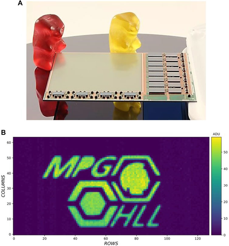
FIGURE 13. (A) Photo of an EDET Quadrant matrix with 512 × 512 pixels of 60 × 60 × 60 μm2 size, integrated on an ASM together with passives and front end electronics. (B) Example image taken with a prototype matrix on a TEM using a shadow mask.
The sensors are read out using readout-on-demand, reading a total number of four pixel rows, i.e., two couple rows, in parallel with an advanced timing of 100 ns per readout. In this way, a complete sensor matrix of 512 × 512 pixels can be read in 12.8 µs. The system uses drain readout, using the so-called DCD-E IC as front-end, a 256 channel TIA/digitizer IC with a resolution of 8 bit. Each DCD hands its digitized data over to one digital sequencer/buffer IC of type DMC, which stores the data before it is transferred to the peripheral data acquisition system using a 1.6 GHz AURORA link. In this way, bursts of up to 50 images with maximum time resolution can be acquired. Using selective readout of window ROIs, both (window) framerate and number of images per burst increase by the same factor.
4 Summary
Three different approaches for dealing with the increasing demands on photon science instrumentation, currently under development at the MPG HLL were presented. Especially challenging is meeting the requirements on dynamic range at low and high end simultaneously. Optimum solutions here require sophisticated front-end electronics and detector structures capable of applying customized nonlinear gain characteristics.
The newly developed MARTHA structures, a new type of APD arrays operated in low gain, overcome traditional drawbacks of APD arrays and have the potential to increase the low energy detection limit by applying avalanche multiplication. If combined with multilinear front-end electronics, they could serve as drop-in replacement for existing pad or pixel detector based solutions for hybrid pixel detector systems.
New operation modes for pnCCDs allow to drastically increase their CHC up to the point where they become interesting for high contrast photon science measurement. They can offer a technologically simple solution for covering large areas in applications, where framerate is not the main driver. To accommodate for the high dynamic range, DEPFET based EOC amplifiers with nonlinear gain are used to customize the dynamic range to the requirements. The use of DEPFET based EOCs here also helps to increase readout speed of the CCDs.
Finally, DEPFET active pixel arrays offer the potential to combine nonlinear gain, implemented in each pixel, with multiple possible readout modes. Systems implementing full parallel readout as well as four-fold multiparallel readout have already been implemented. In addition to its potentially higher readout speed, the DEPFET also offers higher flexibility in terms of readout modes, e.g., reading of windows and ROIs, and pixel sizes. In case of a one- or twofold multiparallel readout, however, a pnCCD using the DEPFET only as EOC amplifier could be an alternative, if no advanced readout modes and pixel sizes within a certain range are requested.
Although not discussed in this paper, modularity is another important prerequisite for photon science detectors. Many experiments benefit from large solid angles, so assembling large composite focal planes from multiple smaller detector modules with minimum dead area is an important capability. Most hybrid pixel detectors are build that way, but also pnCCDs and DEPFET pixel arrays can be used for building highly integrated, compact, 4-side buttable sensor tiles. The required advanced mechanical and thermal support structures have been successfully prototyped.
Author contributions
JN: Conceptualization, Writing–original draft, Writing–review and editing. AB: Conceptualization, Investigation, Methodology, Writing–original draft, Writing–review and editing. RR: Conceptualization, Investigation, Methodology, Writing–original draft, Writing–review and editing. JT: Conceptualization, Investigation, Methodology, Writing–original draft, Writing–review and editing.
Funding
The author(s) declare that no financial support was received for the research, authorship, and/or publication of this article.
Conflict of interest
The authors declare that the research was conducted in the absence of any commercial or financial relationships that could be construed as a potential conflict of interest.
Publisher’s note
All claims expressed in this article are solely those of the authors and do not necessarily represent those of their affiliated organizations, or those of the publisher, the editors and the reviewers. Any product that may be evaluated in this article, or claim that may be made by its manufacturer, is not guaranteed or endorsed by the publisher.
References
1. Hart M, Angelsen C, Burge S, Coughlan J, Halsall R, Koch A, et al. Development of the LPD, a high dynamic range pixel detector for the European XFEL. In: Proceedings of the 2012 IEEE Nuclear Science Symposium and Medical Imaging Conference Record (NSS/MIC); November 2012; Anaheim, CA, USA (2012). p. 534–7. doi:10.1109/NSSMIC.2012.6551165
2. Allahgholi A, Becker J, Bianco L, Delfs A, Dinapoli R, Goettlicher P, et al. AGIPD, a high dynamic range fast detector for the European XFEL. J Instrumentation (2015) 10:C01023. doi:10.1088/1748-0221/10/01/C01023
3. Photonics Online. Silicon avalanche photodiode (APD) arrays (2024). Available at: https://www.photonicsonline.com/doc/silicon-avalanche-photodiode-apd-arrays-0001.
4. Pellegrini G, Fernandez-Martinez P, Baselga M, Fleta C, Flores D, Greco V, et al. Technology developments and first measurements of low gain avalanche detectors (LGAD) for high energy physics applications. Nucl Instrum Methods A (2014) 765:12–6. doi:10.1016/j.nima.2014.06.008
5. Cartiglia N, Arcidiacono R, Boscardin M, Dalla Betta GF, Cartiglia N, Cenna F, et al. Design optimization of ultra-fast silicon detectors. Nucl Instrum Meth A (2015) 796:141–8. doi:10.1016/j.nima.2015.04.025
6. Sadrozinski H-W, Baselga M, Ely S, Fadeyev V, Galloway Z, Ngo J, et al. Ultra-fast silicon detectors. Nucl Instrum Meth A (2014) 765:226–31. doi:10.1016/j.nima.2013.06.033
7. Paternoster G, Borghi G, Arcidiacono R, Boscardin M, Cartiglia N, Centis Vignali M, et al. Novel strategies for fine-segmented low gain avalanche diodes. Nucl Instrum Meth A (2021) 987:164840. doi:10.1016/j.nima.2020.164840
8. Zhang J, Barten R, Baruffaldi F, Bergamaschi A, Borghi G, Boscardin M, et al. Development of LGAD sensors with a thin entrance window for soft X-ray detection. JINST (2022) 17:C11011. doi:10.1088/1748-0221/17/11/C11011
9. Cartiglia N, Arcidiacono R, Borghi G, Boscardin M, Costa M, Galloway Z, et al. LGAD designs for future particle trackers. Nucl Instrum Meth A (2020) 979:164383. doi:10.1016/j.nima.2020.164383
10. Zhao Y, Ayyoub S, Chen W, Gee C, Islam R, Mazza M, et al. A new approach to achieving high granularity for silicon diode detectors with impact ionization gain. J Phys Conf Ser (2022) 2374:012171. doi:10.1088/1742-6596/2374/1/012171
11. McIntyre RJ. Recent developments in silicon avalanche photo-diodes. Measurement (1985) 3:146–52. doi:10.1016/0263-2241(85)90024-7
12. Synopsys TCAD. TCAD solutions (2024). Available at: www.synopsys.com/manufacturing/tcad.html.
13. van Overstraeten R, DeMan H. Measurement of the ionization rates in diffused silicon p-n junctions. Solid-State Electro (1970) 13:583–608. doi:10.1016/0038-1101(70)90139-5
14. Ebermayer S, Andritschke R, Elbs J, Meidinger N, Strüder L, Hartmann R, et al. Quantum efficiency measurements of eROSITA pnCCDs. Proc SPIE (2010) 7742:77420U. doi:10.1117/12.856939
15. Currás E, Fernández M, Moll M. Gain reduction mechanism observed in low gain avalanche diodes. Nucl Instrum Meth A (2022) 1031:166530. doi:10.1016/j.nima.2022.166530
16. Jansen F, Lumb D, Altieri B, Clavel J, Ehle M, Erd C, et al. XMM-Newton observatory. A&A (2001) 365:L1–6. doi:10.1051/0004-6361:20000036
17. Strüder L, Brie U, Dennerl K, Hartmann R, Kendziorra E, Meidinger N, et al. The European photon imaging camera on XMM- Newton: the pn-CCD camera. A&A (2001) 365:L18–26. doi:10.1051/0004-6361:20000066
18. Merloni A, Predehl P, Becker W, Böhringer H, Boller T, Brunner H. eROSITA science book: mapping the structure of the energetic universe (2012). Available at: https://arxiv.org/abs/1209.3114.
19. Erk B, Müller JP, Bomme C, Boll R, Brenner G, Chapman HN, et al. CAMP@FLASH: an end-station for imaging, electron and ion-spectroscopy, and pump-probe experiments at the FLASH free-electron laser. J Synchrotron Radiat (2018) 25:1529–40. doi:10.1107/S1600577518008585
20. Osipov T, Bostedt C, Castagna J-C, Ferguson KR, Bucher M, Montero SC, et al. The LAMP instrument at the linac coherent light source free-electron laser. Rev Scientific Instr (2018) 89:035112. doi:10.1063/1.5017727
21. Strüder L, Epp S, Rolles D, Hartmann R, Holl P, Lutz G, et al. Large-format, high-speed, X-ray pnCCDs combined with electron and ion imaging spectrometers in a multipurpose chamber for experiments at 4th generation light sources. NIMA (2010) 614:483–96. doi:10.1016/j.nima.2009.12.053
22. Schmidt J, Hartmann R, Holl P, Huth M, Lutz G, Soltau J, et al. Dynamic range of fully depleted pnCCDs: modeling and experimental confirmation. Proc SPIE (2014) 9154. doi:10.1117/12.2055343
23. Meidinger N, Bonerz S, Eckhardt R, Englhauser J, Hartmann R, Hasinger G, et al. First measurements with a frame store PN-CCD X-ray detector. NIMA (2003) 512:341–9. doi:10.1016/S0168-9002(03)01912-0
24. Hermann S, Buttler W, Hartmann R, Meidinger N, Porro M, Strueder L, et al. CAMEX readout ASICs for pnCCDs. In: Proceedings of the 2008 IEEE Nuclear Science Symposium Conference Record; October 2008; Dresden, Germany (2008). doi:10.1109/NSSMIC.2008.4774983
25. Porro M, Bianchi D, De Vita G, Hartmann R, Hauser G, Hermann S, et al. VERITAS: a 128-channel asic for readout of pnCCDs and DEPFET arrays for X-ray imaging, spectroscopy and XFEL applications. IEEE TNS (2013) 60(1):446–55. doi:10.1109/TNS.2012.2228410
26. Chapman H, Fromme P, Barty A, White TA, Kirian RA, Aquila A, et al. Femtosecond X-ray protein nanocrystallography. Nature (2011) 470:73–7. doi:10.1038/nature09750
27. Kemmer J, Lutz G. New detector concepts. NIMA (1987) 253:365–77. doi:10.1016/0168-9002(87)90518-3
28. Prereira DE. DePFET active pixel sensors for the vertex detector of the Belle-II experiment. JINST (2013). doi:10.1088/1748-0221/9/03/C03004
29. Ye H, Abudinen F, Ackermann K, Ahlburg P, Albalawi M, Alonso O, et al. Commissioning and performance of the Belle II pixel detector. NIM A (2021) 987:164875. doi:10.1016/j.nima.2020.164875
30. Meidinger N, Eder J, Fürmetz M, Nandra K, Pietschner D, Strecker R, et al. Development of the wide field imager for athena. Proc SPIE (2015) 9601. doi:10.1117/12.2187012
31. Meidinger N, Barbera M, Emberger V, Fürmetz M, Manhart M, Müller-Seidlitz J, et al. The wide field imager instrument for athena. Proc SPIE (2017) 10397. doi:10.1117/12.2271844
32. BunceMartindale EJA, Lindsay S, Muinonen K, Rothery DA, Pearson J, McDonnel I, et al. The BepiColombo mercury imaging X-ray spectrometer: science goals, instrument performance and operations. Space Sci Rev (2020) 216:126. doi:10.1007/s11214-020-00750-2
33. Majewski P, Andricek L, Christensen U, Hilchenbach M, Lauf T, Lechner P, et al. DEPFET macropixel detectors for MIXS: first electrical qualification measurements. IEEE Trans Nucl Sci (2010) 57(4):2389–96. doi:10.1109/TNS.2010.2053557
34. Maffessanti S, Hansen K, Aschauer S, Castoldi A, Erdinger F, Fiorini C, et al. A 64k pixel CMOS-DEPFET module for the soft X-rays DSSC imager operating at MHz-frame rates. Sci Rep (2023) 13:11799. doi:10.1038/s41598-023-38508-9
35. Andricek L, Bähr A, Lechner P, Ninkovic J, Richter RH, Schopper F, et al. DePFET -recent developments and future prospects. Front Phys Sec Radiat Detectors Imaging (2022) 10. doi:10.3389/fphy.2022.896212
36. Bähr A, Feller A, Lechner P, Ninkovic J, Richter R, Schopper F, et al. Advanced DePFET concepts: quadropix. NIM A (2018) 912:70–4. doi:10.1016/j.nima.2017.10.048
37. Lechner P, Andricek L, Aschauer S, Bähr A, De Vita G, Hermenau K, et al. DEPFET active pixel sensor with non-linear amplification. In: Proceedings of the 2011 IEEE Nuclear Science Symposium Conference Record; October 2011; Valencia, Spain (2011). doi:10.1109/NSSMIC.2011.6154112
38. Aschauer S, Majewski P, Lutz G, Soltau H, Holl P, Hartmann R, et al. First results on DEPFET Active Pixel Sensors fabricated in a CMOS foundry—a promising approach for new detector development and scientific instrumentation. JINST (2017) 12:P11013. doi:10.1088/1748-0221/12/11/P11013
39. Predikaka M, Bähr A, Koffmane C, Ninkovic J, Prinker E, Richter R, et al. EDET DH80k - characterization of a DePFET based sensor for TEM direct electron imaging. NIM A (2020) 958:162544. doi:10.1016/j.nima.2019.162544
40. Predikaka M. Characterization of a novel DePFET based sensor for an ultra-fast Transmission Electron Microscopy application. PhD Thesis. Munich, Germany: Technische Universität München (2022). Available at: https://nbn-resolving.de/urn/resolver.pl?urn:nbn:de:bvb:91-diss-20220627-1656556-1-5.
41. Dourki I. Development of a novel electron detector with 80 kHz frame rate for imaging applications: simulation of the detector response and first experimental results. PhD Thesis. Hamburg, Germany: University of Hamburg (2019). Available at: https://ediss.sub.uni-hamburg.de/handle/ediss/6325.
Keywords: photon science, silicon sensors, APD, DEPFET, pnCCD, pixel detectors, X-rays
Citation: Ninkovic J, Bähr A, Richter RH and Treis J (2024) Novel sensor developments for photon science at the MPG semiconductor laboratory. Front. Phys. 12:1321164. doi: 10.3389/fphy.2024.1321164
Received: 13 October 2023; Accepted: 09 January 2024;
Published: 23 January 2024.
Edited by:
Jiaguo Zhang, Paul Scherrer Institut (PSI), SwitzerlandReviewed by:
Giacomo Borghi, Polytechnic University of Milan, ItalyJonathan Correa, Helmholtz Association of German Research Centres (HZ), Germany
Copyright © 2024 Ninkovic, Bähr, Richter and Treis. This is an open-access article distributed under the terms of the Creative Commons Attribution License (CC BY). The use, distribution or reproduction in other forums is permitted, provided the original author(s) and the copyright owner(s) are credited and that the original publication in this journal is cited, in accordance with accepted academic practice. No use, distribution or reproduction is permitted which does not comply with these terms.
*Correspondence: J. Ninkovic, Jelena.ninkovic@hll.mpg.de