Wideband hybrid metamaterial absorber via compound design of multiple mechanisms
 Zhenxu Wang1,2†
  Xinmeng Xiong1† Jian-Gang Liang1*
  Jiafu Wang2*
  Xinmin Fu2 Chang Ding2
  Yajuan Han2 Yong Sun2 Yudeng Wang2 Junxiang Zhou2 Juanna Jiang2
  Wenjie Wang2 Shaobo Qu2
- 1Air and Missile Defense College, Air Force Engineering University, Xi’an, Shaanxi, China
- 2Shaanxi Key Laboratory of Artificially-Structured Functional Materials and Devices, Air Force Engineering University, Xi’an, Shaanxi, China
Broadband and high efficiency are the two core indexes of absorption research, which usually requires a balance between them. Therefore, how to take into account both and achieve broadband and efficient absorption is a hot topic in current research. In this paper, by the compound design of multiple mechanisms, a kind of wideband hybrid metamaterial absorber (HMA) is proposed. The overall structure consists of a layer of patterned resistive film and a layer of magnetic absorbing material (MAM) separated by the air. The resistive layer is designed as square ring type to regulate the local magnetic field, which results in significant magnetic field enhancement within the MAM layer, and this mechanism provides a prerequisite for wideband and high-efficiency absorption in the low frequency band. Furthermore, due to the electrical losses of the resistive film, another absorption band is additionally excited in the high frequency band. Thanks to the multiple mechanisms, the absorption efficiency above 90% in the 3.2–22.0 GHz frequency band can be realized, and the thickness of the overall structure is 7.0 mm that is 0.07 of the wavelengths at the lowest frequency point. To demonstrate this method, a prototype is designed, fabricated and measured. Both the simulation and experiment results verify the effectiveness of the proposed method. This work provides a new method to design wideband and high-efficiency electromagnetic absorption structures and may find potential applications in multi-functional planar or conformal structures.
Introduction
Originated from the technology of radar stealth for the military targets, the research of radar absorbing technology has been one of the hottest topics in recent years. As an important and efficient electromagnetic (EM) wave absorbing method, radar absorbing materials (RAMs) have been widely used not only in the military fields, for example, electromagnetic interference shield (EMI), the radar reflection cross section (RCS) reduction [1–3], but also in the civil fields such as solar energy harvesting, biological sensing, thermophotovoltaics, photodetection and so on [4–8]. The traditional RAMs, especially for magnetic absorbing materials (MAMs), which are generally comprised of magnetic metals or ferrite nanocrystalline particles dispersed in a polymer matrix and are based on the strong absorption of the EM, cannot meet the higher and higher requirement of working frequency band and incident angle nowadays.
Metamaterial, as a method to design artificial material, provides a train of thoughts and design concepts to realize some peculiar physical phenomena and effects that are impossible or very hard to be achieved in natural materials including negative refractive index [9], EM wave cloaking [10], inverse Doppler effect [11], and so on. As a new methodology of artificial medium, metamaterials have been widely used in many fields, such as super-lenses, invisibility cloaks, and perfect absorbers [12–14]. For the field of RAMs, on account of the efficient absorption and flexible design, metamaterial absorber (MA) has always been a hot spot at home and abroad, which has been widely used in many pivotal fields such as radar stealth techniques, image sensing, energy harvesting, thermal emission control [15–17] and so on. Recently, Landy et al. designed a new-style MA which can achieve a simulated absorptivity of 99% at specific frequency by using split ring resonators (SRRs) on the top of a dielectric substrate backed with copper strips [14]. Since then, MAs with the configuration of metal-insulator-metal, which based on electric or magnetic resonance and have unique advantages of flexibly adjustable absorption frequency by merely changing geometrical parameters of the unit cell, have obtained considerable development. However, the bandwidth of this kind of MAs is too narrow for its application. After that, MAs with broad operating bandwidth and high absorbing efficiency simultaneously have always been persistently pursued in this topic. A lot of methods have been come up with and a lot of researches have been conducted. For example, in refer [18], an ultrathin tunable MA combining magnetic nanomaterials and metamaterial resonant structures for use in the lower microwave band (P band) was proposed, and by utilizing electrically controlled varactors and replacing the dielectric slabs with magnetic nanomaterials, the proposed absorber can achieve band tunability at low frequencies as well as thickness reduction. Moreover, in refer [19], a 3D structure MA with the folded resistive patches was proposed, which can achieve efficient 90% absorptivity in the frequency band of 3.6–11.4 GHz. Furthermore, via compound design of metamaterials and conventional MAM, the operating bandwidth of hybrid absorbers can be further expanded, such as in refer [20], a two-layer metamaterial absorber consisting of a nonplanar metamaterial and a layer of MAM was proposed, which can realize 90% absorptivity over the whole 4.5–18 GHz range. However, these proposals with the broadband and efficient absorptivity just concentrate on extending the absorption bandwidth to high frequency bands, while solutions addressing low-frequency absorption always tend to rely only on an increase in total thickness.
In this paper, via compound design of multiple mechanisms, a kind of wideband hybrid metamaterial absorber (HMA) is proposed. The overall structure consists of a layer of patterned resistive film and a layer of MAM separated by the air. The resistive layer is designed as square ring type to regulate the local magnetic field, which results in significant magnetic field enhancement within the MAM layer, and this mechanism provides a prerequisite for wideband and high-efficiency absorption in the low frequency band. Furthermore, due to the electrical losses of the resistive film, another absorption band is additionally introduced in the high frequency band. Thanks to the multiple mechanisms, the absorption efficiency above 90% in the 3.2–22.0 GHz frequency band can be realized, and the thickness of the overall structure is 7.0 mm that is 0.07 of the wavelengths at the lowest frequency point. To demonstrate this method, a prototype is designed, fabricated and measured. Both the simulation and experiment results verify the effectiveness of the proposed method. This work provides a new method to design wideband and high-efficiency electromagnetic absorption structures and may find potential applications in multi-functional planar or conformal structures.
Model analysis
The schematics and working principles of the proposed wideband HMA are shown in Figure 1. Clearly, the overall structure consists of a layer of patterned resistive film and a layer of MAM separated by the air and the metal plate. The upper resistive layer is designed as square ring type to regulate the local magnetic field. This mechanism results in significant magnetic field enhancement within the MAM layer, which provides a prerequisite for wideband and high-efficiency absorption in the low frequency band. Furthermore, due to the electrical losses of the resistive film, another absorption band is additionally introduced in the high frequency band. Therefore, derived from the high magnetic loss of the MAM and electrical loss of the resistive layers, wideband and high-efficiency absorption can be achieved. In addition, the symmetrical lattice enables the overall structure to have satisfactory stability for polarization.
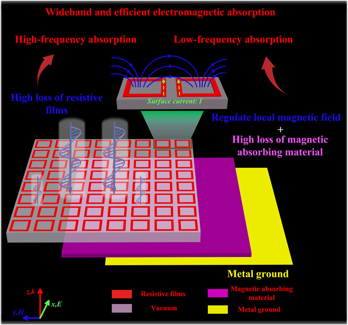
FIGURE 1. The schematics and working principles of the proposed HMA.
Unit structure design and analyze
In our previous work [21], the mechanism called magnetic squeezing effect has been explored, which means that, in the positive resonance region of EM metamaterials, a strong magnetic squeezing effect will occur and more concentrated magnetic field lines will be confined in the EM metamaterials. And this mechanism has been proved to have a wide range of application scenarios in the MAs, particularly in the design of composites of EM metamaterials and MAMs. Actually, according to Faraday’s law of electromagnetic induction, the effect can be excited by any structures that can be capable of generating surface currents, but only varies in intensity. We take the short metallic wire as an example. Just as shown in Figure 2, the schematic diagrams of a meta-atom containing one short metal wire and two short metal wires are given in Figures 2A,B, respectively. The Figures 2Ai,Bi are the top views, while the Figures 2Aiii,Biii are the side views. Figures 2Aii,Bii show the surface current distributions at 13.0 GHz under the x-polarized waves illumination. Similarly, Figures 2Aiv,Biv show the magnetic field distributions at 13.0 GHz under the x-polarized waves illumination. Clearly, whether a meta-atom contains one short metal wire or two short metal wires, surface currents will be induced in the structure surface under the EM waves irradiating, and according to Faraday’s law of electromagnetic induction, the local magnetic field near the metal wires will be modulated, as we expected before. Furthermore, when a meta-atom contains two short metal wires, the surface currents on the two short metal wires flow in the same direction. Comparing the magnetic field distribution in Figures 2Aiv,Biv, we can see that the local magnetic field under the metal wires in Figure 2Biv is slightly stronger than the local magnetic field in Figure 2Aiv, that is to say, the local magnetic field can be modulated more strongly when the number of short metal wires in one meta-atom is increased.
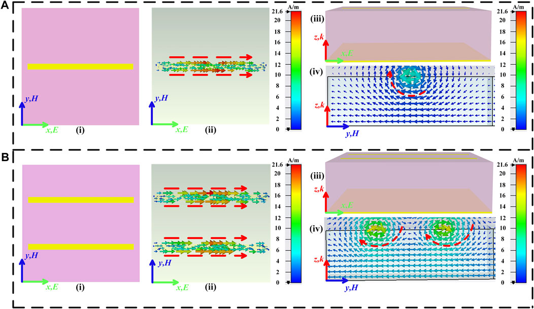
FIGURE 2. The schematic diagrams of a meta-atom containing (A) one short metal wire and (B) two short metal wires: (i) top view; (ii) the surface current distributions; (iii) side view; (iv) magnetic field distributions.
The above is a qualitative analysis of the magnetic squeezing effect excited by the short metal wires. In order to analyze this effect from a quantitative point of view, we replaced a portion of the air beneath the metal wire with a layer of MAM (the thickness is 1.0 mm), as shown in Figure 3. Figures 3A,B show a comparison of the front view of the two states, respectively. Figure 3C shows the reflectivity comparisons. The blue curve represents the reflectivity of the situation of only the short metal wire, as can be seen from the small graph inlaid inside Figure 3C, due to the overall structure being lossless and the resonance of the short metal line occurs around 13.0 GHz, there is a slight variation around 13.0 GHz. The black curve shows the reflectivity of the 1.0 mm thickness MAM layer, which shows a certain degree of attenuation throughout the frequency band due to its magnetic loss. Correspondingly, the red curve shows the reflectivity of the composite of the short metal wire and the MAM layer, which shows a further attenuation in the wide frequency band up to 14.6 GHz. Especially near the 13.1 GHz, the reflectivity is further attenuated by more than 10 dB. Furthermore, as can be seen from Figure 3C, when the frequencies above 14.6 GHz, compared to the MAM, the reflectivity attenuation of the composite structure decreases instead. After analysis, the reason is that when the frequency exceeds 14.6 GHz, it will be in the negative region of the resonance of the short metal lines. As analyzed in the previous work [20], in the negative region of the resonance, the induced magnetic field will be in the opposite direction to the incident magnetic field, resulting in weakening of the magnetic field strength at the location of the MAM. In order to analyze and verify this theory more intuitively, we monitored the magnetic field distribution at 13.0 GHz (in the positive resonance region) and 16.0 GHz (in the negative resonance region) by utilizing CST simulation software, as shown in Figures 3D,E, respectively. It is clear from Figure 3D that at 13.0 GHz, a strong magnetic squeezing effect occurs and more concentrated magnetic field lines are confined below the short metal wire. Such an effect results in a significant increase of the magnetic field strength at the location where the MAM locating, which is the fundamental condition for the composite structure to have significant reflectivity attenuation near 13.0 GHz. On the contrary, as shown in Figure 3E, at 16.0 GHz, the magnetic field strength at the location of MAM layer becomes weakened, which is why the reflectivity attenuation becomes weaker in the frequency band after 14.6 GHz.
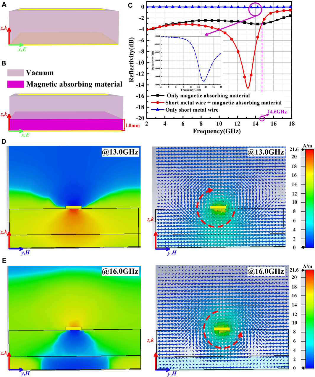
FIGURE 3. The schematic diagrams of a comparison of the front view of the two states: (A) original structure; and (B) a portion of the air beneath the metal wire is replaced by a layer of MAM (the thickness is 1.0 mm). (C) the comparisons of the reflectivity of the 1.0 mm MAM layer, only the short metal wire and the composite of the two. The magnetic field distribution at (D) 13.0 GHz and (E) 16.0 GHz.
Based on the analysis above, a kind of wideband HMA is designed, just as shown in Figure 4A. In order to further expand the absorption bandwidth and achieve polarization-insensitive performance, the overall structure is designed to be symmetrical and the resistive films are used to design as patterned shapes instead of metallic copper. After optimization, the final geometrical parameters are: the periodicity of the meta-atom p = 10.0 mm, l = 8.0 mm, w = 1.0 mm, d1 = 2.0 mm and d2 = 5.0 mm, and the sheet resistance is chosen as: R = 100 Ω/sq. By using CST Microwave Studio 2018, we simulated the reflectivity spectra of the HMA and 2.0 mm thick MAM under normal incidence. The comparison of them is shown in Figure 4B. In the simulation, the boundary conditions along the x- and y-directions are set as the unit cell boundaries, while the z-direction is set as open add space. It is well known that the reflected energy R(ω) and transmitted energy T(ω) can be obtained from the reflection coefficients S11(ω) and transmission coefficients S21(ω), that is, R(ω) = |S11(ω)|2 and T(ω) = |S21(ω)|2, and the absorbed energy A(ω) can be calculated by A(ω) = 1−T(ω)−R(ω) = 1−|S11(ω)|2−|S21(ω)|2. Furthermore, due to the existence of the metal ground, the transmission coefficients S21(ω) = 0 in the frequency range. So, the absorbed energy can be simplified to A(ω) = 1−|S11(ω)|2. That means, the reflectivity spectra can be used to represent the absorption performance. The black curve of the Figure 4B shows the reflectivity of the 2.0 mm thick MAM layer, it is clear that there is only a very narrow absorption band around 5.0 GHz. In contrast, the red curve in the Figure 4B represents the reflectivity of our proposed HMA. The comparison indicates that, in the low-frequency band, by modulating the local magnetic field utilizing the symmetrical square ring type resistive film, not only is the absorption bandwidth effectively extended, but also the absorption efficiency is greatly improved. In addition, in the high-frequency band, a wide absorption bandwidth is additionally introduced due to the electrical losses of the resistive film. As a result, under normal incidence, the −10 dB frequency band is extended to 3.2–22 GHz.
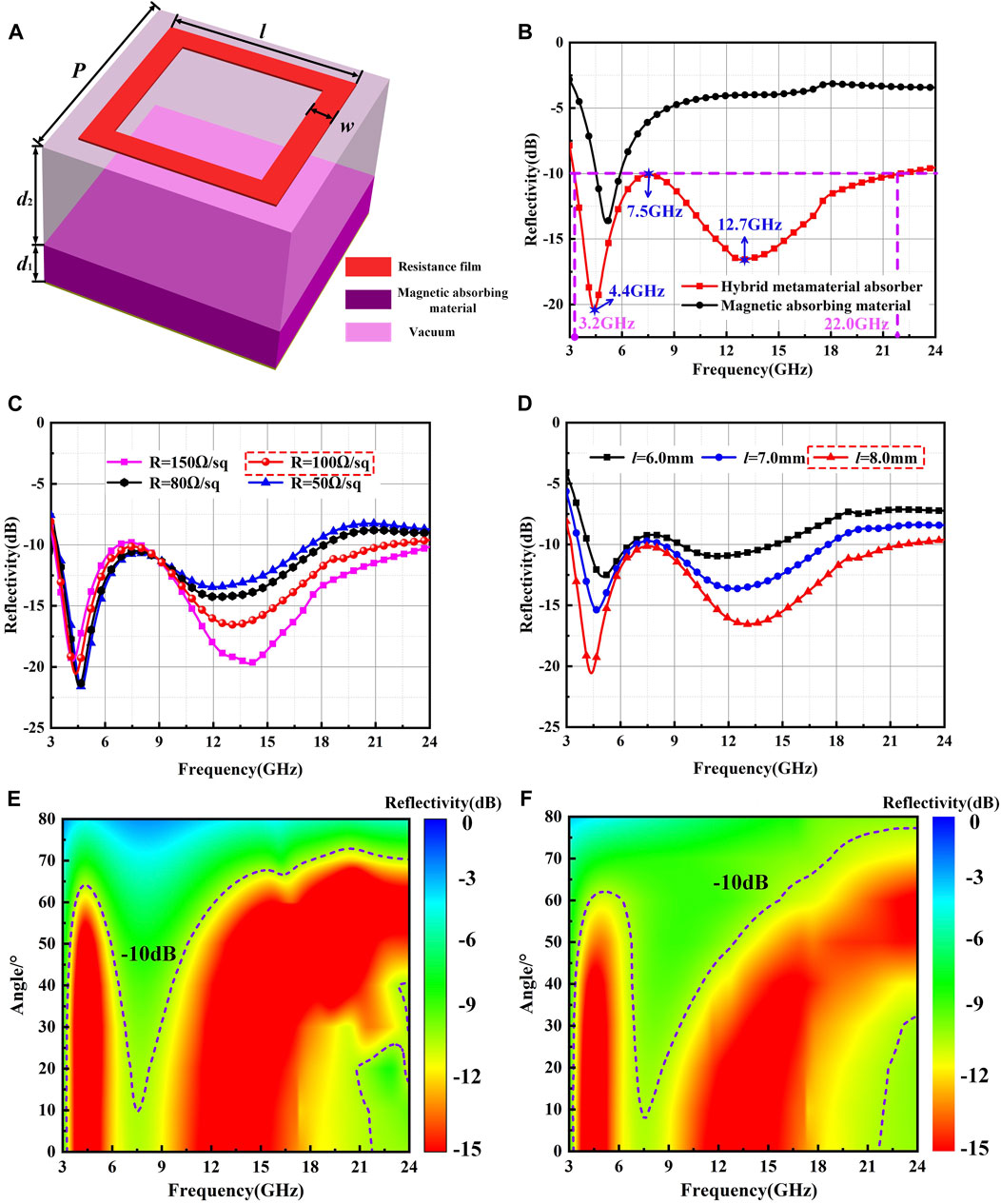
FIGURE 4. (A) Schematic illustration of the unit of proposed HMA. (B) The comparison of the reflectivity of the proposed HMA (the red curve) and 2.0 mm thick MAM (the black curve) under normal incidence. The comparison of the reflectivity with the variation of (C) the sheet resistance value R and (D) the length l. The simulated reflectivity spectra of the proposed HMA at different angles under (E) TE polarized waves and (F) TM polarized waves.
In addition, in the Figure 4C, we give a comparison of the reflectivity of the HMA with the variation of the sheet resistance value R of the resistive film while other geometrical parameters remain constant. It is obvious that with the gradual increase of the sheet resistance value, in the high frequency band, not only the absorption efficiency of the hybrid metamaterial absorber is gradually enhanced, but the absorption bandwidth is also gradually widened. However, as for the low frequency band, the absorption condition is almost unchanged. This is consistent with our design concept that by replacing metallic copper with resistive film to design the patterned shapes, an additional absorption band in the high frequency band can be introduced. Also, in Figure 4D, a comparison of the reflectivity of the HMA with the variation of the edge length l when other geometrical parameters remain constant. Clearly, as the edge length l decreasing, in the low frequency band, due to the weaker modulation of the local magnetic field, the absorption efficiency of the hybrid metamaterial absorber becomes weaker, and for the high frequency band, since the electrical loss of the resistive film becomes weaker, the absorption efficiency is correspondingly weaker. Furthermore, the reflectivity spectra of the proposed HMA varied with different incident angles for TE and TM polarized waves are shown in Figures 4E,F, respectively. Clearly, we can see that, the absorptivity has a high stability in both TE and TM modes for normal incidence. However, as the angle of incidence increases, for TE mode, the electric field component remains unchanged and the transverse magnetic field component is decreasing, so the absorption bandwidth in the low frequency band will decrease, and the high absorption band will move to higher frequency band. For TM mode, as the angle of incidence increases, the transverse magnetic field component remains unchanged and the electric field component is decreasing, so the low absorption band will remain unchanged, and the absorption bandwidth in the high frequency band will decrease.
In order to further verify our design strategy, by utilizing CST Microwave Studio 2018, we monitored the magnetic field distribution and surface current distribution of several typical frequency points, as shown in Figure 5. The Figures 5A,C represent the magnetic field distribution and surface current distribution of 4.4 GHz. Consistent with the previous analysis in Figures 2, 3, at 4.4 GHz, the surface currents flow in the same direction on both sides of the square ring, and an obvious magnetic squeezing effect occurs. More concentrated magnetic field lines are confined below the square ring type resistive film, resulting in a significant increase of the magnetic field strength at the location where the MAM locating and a significant reflectivity attenuation near the frequency point. The magnetic field distribution of 7.5 GHz is depicted in Figure 5B. Different from the Figure 5A, the magnetic field strength at the location of MAM layer becomes weakened, which is corresponding to a decrease of the absorption efficiency. The Figure 5D also shows the surface current distribution of 12.7 GHz. Clearly, there is a significant increase in surface current intensity on the square ring, and derived from the high electrical losses of the resistive film, in high frequency band, efficient absorption can be realized. Moreover, we also monitored the energy dissipation distribution at 4.4 GHz and 12.7 GHz, which were shown in Figures 5E,F, respectively. Obviously, at 4.4G Hz, the energy of the incident wave is mainly dissipated in the underlying MAM. And, at 12.7 GHz, most energy of the incident wave is mainly dissipated in the resistive film. This is consistent with the previous results for the magnetic field distribution and surface current distribution.
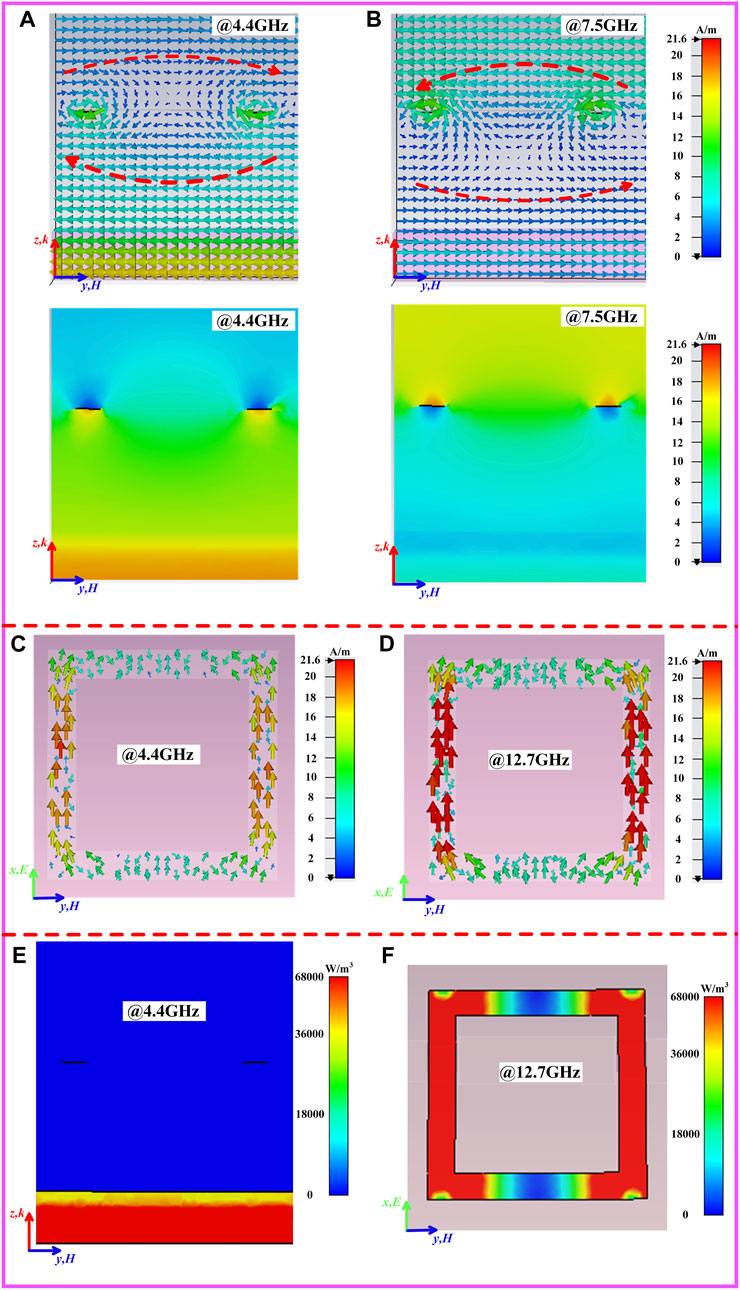
FIGURE 5. The magnetic field distribution of (A) 4.4 GHz and (B) 7.5 GHz. The surface current distribution of (C) 4.4 GHz and (D) 12.7 GHz. The energy dissipation distribution of (E) 4.4 GHz and (F) 12.7 GHz.
Experimental verification
In order to verify our design concept, a prototype of the proposed HMA with the area of 400 × 400 mm2 is fabricated and measured, which is shown in Figure 6A. The components from top to bottom are: square ring type resistive film, PMI foam, MAM with 2.0 mm thickness and metal ground. As is shown in the Figure 6A, the experiment was conducted, in the microwave anechoic chamber, the experiment was conducted. Since the structure is symmetric and polarization-insensitive, for convenience, we only measured the reflectivity curve under one polarization. Under normal incidence, the comparison between the simulated and measured reflectivity curves is given in Figure 6B. Clearly, considering the tolerance in the fabrication and experiment, the trend of both was the same, therefore, we can agree that our proposed HMA can achieve wideband and efficient absorption in 3.2–22.0 GHz.
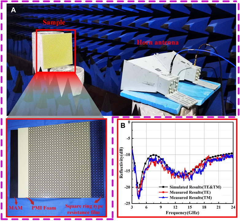
FIGURE 6. (A) The fabricated prototype of proposed HMA and the measured environment. (B) The comparison between the simulated and measured reflectivity curves.
Conclusion
In conclusion, via compound design of multiple mechanisms, a kind of wideband HMA is designed, fabricated and measured. The overall structure consists of a layer of patterned resistive film and a layer of MAM separated by the air. The resistive layer is designed as square ring type to regulate the local magnetic field, which results in significant magnetic field enhancement within the MAM layer, and this mechanism provides a prerequisite for wideband and high-efficiency absorption. Furthermore, due to the electrical losses of the resistive film, another absorption band is additionally introduced in the high frequency band. Thanks to the multiple mechanisms, the absorption efficiency above 90% in the 3.2–22.0 GHz frequency band can be realized, with a bandwidth around 1:7 and the thickness of the overall structure is 7.0 mm that is 0.07 of the wavelengths at the lowest frequency point. To demonstrate this method, a prototype is designed and fabricated, both the simulation and experiment results verify the effectiveness of the proposed method. This work provides a new method to design wideband and high-efficiency electromagnetic absorption structures and may find potential applications in multi-functional planar or conformal structures.
Data availability statement
The original contributions presented in the study are included in the article/supplementary material, further inquiries can be directed to the corresponding authors.
Author contributions
ZW: Writing–original draft, Writing–review & editing. XX: Writing–review & editing. J-GL: Writing–review & editing. JW: Writing–review & editing. XF: Writing–review & editing. CD: Writing–review & editing. YH: Writing–review & editing. YS: Writing–review & editing. YW: Writing–review & editing. JZ: Writing–review & editing. JJ: Writing–review & editing. WW: Writing–review & editing. SQ: Writing–review & editing.
Funding
The author(s) declare financial support was received for the research, authorship, and/or publication of this article. This work was supported by the National Natural Science Foundation of China under Grant Nos. 61971435, 62101588 and 61971437, the National key Research and Development Program of China under Grant No. 2022YFB3806200.
Conflict of interest
The authors declare that the research was conducted in the absence of any commercial or financial relationships that could be construed as a potential conflict of interest.
Publisher’s note
All claims expressed in this article are solely those of the authors and do not necessarily represent those of their affiliated organizations, or those of the publisher, the editors and the reviewers. Any product that may be evaluated in this article, or claim that may be made by its manufacturer, is not guaranteed or endorsed by the publisher.
References
1. Liu T, Cao X, Gao J, Zheng Q, Li W, Yang H. RCS reduction of waveguide slot antenna with metamaterial absorber. IEEE Trans antennas propagation (2012) 61(3):1479–84. doi:10.1109/tap.2012.2231922
2. Wang Z, Fu X, Wang J, Fan Y, Li Y, Yan M, et al. Multi-octave radar cross section reduction via integrated dispersion engineering of polarization-conversion metasurface and metamaterial absorber. J Phys D: Appl Phys (2019) 53(3):03LT01. doi:10.1088/1361-6463/ab50e4
3. Iwaszczuk K, Strikwerda AC, Fan K, Zhang X, Averitt RD, Jepsen PU. Flexible metamaterial absorbers for stealth applications at terahertz frequencies. Opt express (2012) 20(1):635–43. doi:10.1364/oe.20.000635
4. Hao J, Wang J, Liu X, Padilla WJ, Zhou L, Qiu M. High performance optical absorber based on a plasmonic metamaterial. Appl Phys Lett (2010) 96(25):251104. doi:10.1063/1.3442904
5. Reinhard B, Schmitt KM, Wollrab V, Neu J, Beigang R, Rahm M. Metamaterial near-field sensor for deep-subwavelength thickness measurements and sensitive refractometry in the terahertz frequency range. Appl Phys Lett (2012) 100(22):221101. doi:10.1063/1.4722801
6. Yong Z, Zhang S, Gong C, He S. Narrow band perfect absorber for maximum localized magnetic and electric field enhancement and sensing applications. Scientific Rep (2016) 6(1):24063–7. doi:10.1038/srep24063
7. Wu C, Neuner B, John J, Milder A, Zollars B, Savoy S, et al. Metamaterial-based integrated plasmonic absorber/emitter for solar thermo-photovoltaic systems. J Opt (2012) 14(2):024005. doi:10.1088/2040-8978/14/2/024005
8. Shrekenhamer D, Xu W, Venkatesh S, Schurig D, Sonkusale S, Padilla WJ. Experimental realization of a metamaterial detector focal plane array. Phys Rev Lett (2012) 109(17):177401. doi:10.1103/physrevlett.109.177401
9. Smith DR, Padilla WJ, Vier DC, Nemat-Nasser SC, Schultz S. Composite medium with simultaneously negative permeability and permittivity. Phys Rev Lett (2000) 84(18):4184–7. doi:10.1103/physrevlett.84.4184
10. Chen H, Wu BI, Zhang B, Kong JA. Electromagnetic wave interactions with a metamaterial cloak. Phys Rev Lett (2007) 99(6):063903. doi:10.1103/physrevlett.99.063903
11. Seddon N, Bearpark T. Observation of the inverse Doppler effect. Science (2003) 302(5650):1537–40. doi:10.1126/science.1089342
12. Fang N, Zhang X. Imaging properties of a metamaterial superlens. In: Proceedings of the 2nd IEEE Conference on Nanotechnology; August 2002; Washington, DC, USA. IEEE (2002). p. 225–8.
13. Ma HF, Cui TJ. Three-dimensional broadband ground-plane cloak made of metamaterials. Nat Commun (2010) 1(1):21–6. doi:10.1038/ncomms1023
14. Landy NI, Sajuyigbe S, Mock JJ, Smith DR, Padilla WJ. Perfect metamaterial absorber. Phys Rev Lett (2008) 100(20):207402. doi:10.1103/physrevlett.100.207402
15. Wang B, Liu M, Huang T, Zhao C. Micro/nanostructures for far-field thermal emission control: an overview. ES Energ Environ (2019) 6(4):18–38. doi:10.30919/esee8c360
16. Hunt J, Gollub J, Driscoll T, Lipworth G, Mrozack A, Reynolds MS, et al. Metamaterial microwave holographic imaging system. JOSA A (2014) 31(10):2109–19. doi:10.1364/josaa.31.002109
17. Mason JA, Smith S, Wasserman D. Strong absorption and selective thermal emission from a midinfrared metamaterial. Appl Phys Lett (2011) 98(24):241105. doi:10.1063/1.3600779
18. Ning J, Chen K, Zhao W, Zhao J, Jiang T, Feng Y. An ultrathin tunable metamaterial absorber for lower microwave band based on magnetic nanomaterial. Nanomaterials (2022) 12(13):2135. doi:10.3390/nano12132135
19. Shen Y, Pang Y, Wang J, Ma H, Pei Z, Qu S. Origami-inspired metamaterial absorbers for improving the larger-incident angle absorption. J Phys D: Appl Phys (2015) 48(44):445008. doi:10.1088/0022-3727/48/44/445008
20. Li W, Wu T, Wang W, Guan J, Zhai P. Integrating non-planar metamaterials with magnetic absorbing materials to yield ultra-broadband microwave hybrid absorbers. Appl Phys Lett (2014) 104(2). doi:10.1063/1.4862262
Keywords: wideband, metamaterial absorber, high-efficicent, multiple mechanisms, magnetic absorbing material
Citation: Wang Z, Xiong X, Liang J-G, Wang J, Fu X, Ding C, Han Y, Sun Y, Wang Y, Zhou J, Jiang J, Wang W and Qu S (2023) Wideband hybrid metamaterial absorber via compound design of multiple mechanisms. Front. Phys. 11:1301458. doi: 10.3389/fphy.2023.1301458
Received: 25 September 2023; Accepted: 31 October 2023;
Published: 14 November 2023.
Edited by:
Yuxuan Ren, Fudan University, ChinaCopyright © 2023 Wang, Xiong, Liang, Wang, Fu, Ding, Han, Sun, Wang, Zhou, Jiang, Wang and Qu. This is an open-access article distributed under the terms of the Creative Commons Attribution License (CC BY). The use, distribution or reproduction in other forums is permitted, provided the original author(s) and the copyright owner(s) are credited and that the original publication in this journal is cited, in accordance with accepted academic practice. No use, distribution or reproduction is permitted which does not comply with these terms.
*Correspondence: Jian-Gang Liang, cat-liang1975@163.com; Jiafu Wang, wangjiafu1981@126.com
†These authors have contributed equally to this work