A Balanced Tri-Band Substrate Integrated Waveguide Bandpass Filter With High Selectivity
 Li Min
 Mingyue Pan2
  Congcai Xu
- 1School of Information Engineering, Suqian University, Suqian, China
- 2School of Electrical and Automation Engineering, Nanjing Normal University, Nanjing, China
This paper proposed a balanced tri-band bandpass filter (BPF) with high selectivity based on substrate integrated waveguide (SIW) technology. The tri-band filtering response and multiple transmission zeros (TZs) are attained by elaborately merging cascaded quadruplet (CQ) topology and split topology. The proposed balanced tri-band bandpass filter is designed, which integrates high selectivity differential-mode (DM) transmission and good common-mode suppression by cleverly placing TE102-mode SIW cavity on the symmetric plane. To verify the proposed concept, a prototype of balanced tri-band BPF operating at 9.33, 9.67, and 10.02 GHz has been implemented. Measured results show eight TZs at out of DM passbands and more than 35 dB CM suppression within the DM passbands, which agree well with the simulated results.
Introduction
In recent years, balanced circuits are widely used because of their ability of noise suppression and low electromagnetic interference [1]. Specially, balanced bandpass filters (BPFs) with different transmission structures, such as microstrip [2, 3] and patch resonator [4] have attached much attention recently [2]. presents a new fourth-order balanced dual-band bandpass filter (BPF) based on four coupled bi-section half-wavelength (λ/2) stepped-impedance resonators (SIRs) [3]. presents a balanced filter by centrally-loaded half-wavelength resonator. In [4], a novel dual-band balanced BPF is constructed based on patch resonators and meandered slotlines (MSLs). Unfortunately, at high frequencies, these structures which can achieve good CM suppression suffer from high insertion loss and radiation.
To solving this problem, substrate integrated waveguide (SIW) technology which exhibits its inherent advantages of compactness, low insertion loss at high frequency, and high power capacity is widely employed in microwave and millimeter-wave devices [5–8]. To take advantage of these superiorities, some SIW balanced BPFs have been investigated [9–11]. In [9], a dual-band balanced BPF is designed based on 10 cascaded cavities in planar, while its frequency selective is poor. To improve frequency selectivity, both source-to-load and cross-couplings are introduced by implementing four resonant modes in two cavities to design a balanced dual-band SIW BPF [10]. In addition [11], presents another dual-band differential BPF with controllable differential-mode (DM) center frequencies, and high common-mode (CM) suppression. Although the above designs have many advantages in some aspects, they are limited to dual-band case and cannot meet the multiband requirement in the multi-standard wireless system. As far as the author is concerned, there are few design for multi-band SIW balanced BPF, let alone the one with compact size high frequency selectivity.
In this paper, a balanced tri-band SIW BPF with high selectivity is proposed for micro-and millimeter-wave multi-standard application. By intelligently combining CQ topology with splitting topology, the tri-band filtering response and high selectivity can be achieved simultaneously. Meanwhile, the flexible DM transmission and CM rejection characteristics are obtained with reasonable arrangement of SIW cavity and the resonant modes. The measured results are in good agreement with simulated ones which show the advantage of high selectivity.
Balanced Tri-Band Filter Design
Figure 1 depicts the physical configuration of the proposed balanced tri-band BPF. The design consists of a group of SIW cavities with almost same structures in the top and bottom layers. There is a common ground layer between the two layers. Each layer consists of two resonant TE102-mode cavities and four resonant TE101-mode cavities. The two resonant TE102-mode cavities are coupled with each other, and each resonant TE102-mode cavity is cascaded with two resonant TE101-mode cavities, respectively. Circular and rectangular coupling slots are etched on the common ground layer for signal coupling transmission. The balanced BPF is externally fed by the 50 Ω microstrip lines. Figure 2 shows the electric and magnetic field distributions of the TE102-mode in SIW cavity. Obviously, the electric field distribution in the single SIW cavity is odd symmetric with respect to the symmetrical plane (T-T′). The filed characteristic can be fully explored to realize a balanced SIW cavity with DM transmission and CM suppression.
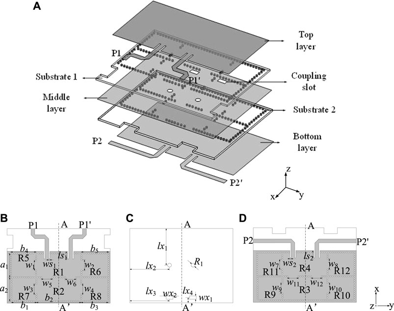
FIGURE 1. Physical configuration of proposed balanced tri-band BPF. (A) 3-D view, (B) top layer, (C) middle layer, (D) bottom layer.
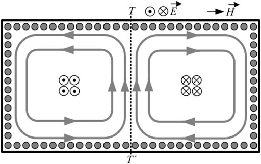
FIGURE 2. Field pattern of TE102-mode in single SIW cavity.
The work mechanism of this design under the DM and CM excitation will be analyzed below. The main structure of the design is composed of four resonant TE102-mode cavities, and the four cavities are arranged according to the CQ topology. Therefore, when the DM signals are injected from the input ports (P1 and P1′) placed at the symmetrical sides of the A-A′ plane, TE102-mode will be excited in resonant cavity 1 (R1). Then, the signal will be transmitted to resonant cavity 2 (R2) in the form of magnetic coupling and excites TE102-mode through the coupling window. Afterwards, the signal in R2 is transmitted to the resonant cavity 3 (R3) in the form of magnetic coupling through the rectangular coupling slots etched in the common ground layer. Subsequently, it is delivered to the resonant cavity 4 (R4) in the form of magnetic coupling through the coupling window. It is worth noting that two circular coupling slots are etched at the middle metal layer with the position where the electric field intensity distribution is strongest in order to achieve electrically coupled transmission between R1 and R4. Finally, the DM signal is obtained by the differential output port (P2 and P2′) in the R4. In addition, each TE102-mode resonator carries two TE101-mode resonators for desired triple-band response. It is worth mention that eight transmission zeros (TZs) are produced in the design of the triple-band response. Among them, the six TZs between the passbands are introduced due to the band-stop resonator while the other two TZs of the stopband on the third passband are caused by cross coupling. When signals at input pairs are CM ones, it is obvious that the CM signal can be converted to two out-of-phase signals which will cancel with each other out through these TE102-mode balanced SIW cavities, thus resulting in the high CM suppression.
Based on the above analysis, Figure 3 describes the schematic coupling topology and equivalent DM topology for the proposed balanced tri-band BPF. In the topology, the white circles S+ and S− represent balanced input pairs P1 and P1′ while the white circles L+ and L− represent the output pairs P2 and P2′, respectively. Besides, the black circles indicate the TE102-modes while the gray circles describe the TE101-modes. The black dashed lines represent electrical coupling while the black solid lines denote magnetic coupling. Its equivalent two-port filter DM topology of the balanced tri-band BPF is shown in Figure 3B. The DM transmission performance is the same as the topology exhibited in Figure 3A.
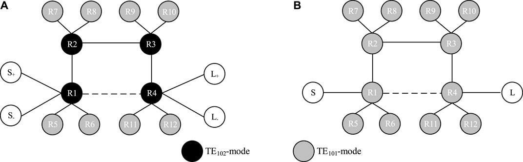
FIGURE 3. Topologies of proposed balanced tri-band BPF. (A) Four-port schematic topology, (B) Equivalent two-port DM topology.
A tri-band balanced BPF is designed with the targeted specifications as follows:
1) Passband 1: 9.17–9.47 GHz (CF: 9.40 GHz, BW: 300 MHz);
2) Passband 2: 9.58–9.77 GHz (CF: 9.69 GHz, BW: 190 MHz);
3) Passband 3: 9.89–10.26 GHz (CF: 9.98 GHz, BW: 370 MHz)
4) TZ1: 9.1 GHz;
5) TZ2: 10.3 GHz;
6) In-band return loss: 20.0 dB.
So the required coupling coefficients and resonator frequencies can be calculated with well-established synthesized method [12] as follows, K1,2 = K3,4 = 0.062,K1,4 = −0.048,K2,3 = 0.079, K1,5 = K2,7 = K3,9 = K4,11 = 0.0356, K1,6 = K2,8 = K3,10 = K4,12 = 0.03418, Qe = 12.56, f01 = f02 = f03 = f04 = 9.7049 GHz, f05 = f07 = f09 = f011 = 9.8338 GHz, f06 = f08 = f010 = f012 = 9.51588 GHz, respectively. The resonator frequencies can be extracted by the size of SIW cavities through eigenmode simulation. While the required internal coupling, external quality factor can be extracted in the following,
where f0i and f0j represent the resonant frequencies of different cavities (R1,R2,R3,R4,R5,R6,R7,R8,R9,R10,R11,R12) respectively, Kij represents the coupling coefficient between the SIW cavity resonators, and τS11 (ω0) represents the S11 group delay corresponding to the resonant frequency point which can be obtained through simulation.
Firstly, the initial parameters of the SIW cavity are determined according to the above analysis. Then, the desired results of the balanced tri-band BPF can be optimized by High Frequency Structure Simulator (HFSS). The final parameters of the proposed balanced tri-band BPF are: a1 = 14.4, a2 = 14.4, b1 = 15, b2 = 26.9, b3 = 16.3, b4 = 15, b5 = 16.3, w1 = 6.2, w2 = 6.4, w3 = 6.3, w4 = 6.4, w5 = 6.5, w6 = 6.5, w7 = 6.2, w8 = 6.4, w9 = 6.3, w10 = 6.4, w11 = 6.5, w12 = 6.5, ls1 = 4.5, ls2 = 4.5, ws1 = 0.65, ws2 = 0.65, lx1 = 8.4, lx2 = 23.9, lx3 = 24, lx4 = 3.2, wx1 = 2, wx2 = 4, R1 = 2.4 (units: mm).
Results and Discussion
The proposed balanced tri-band BPF is fabricated on RT/Duroid 5880 substrate with thinkness of 0.508 mm, εr = 2.2, and tanδ = 0.0009. Figure 4 shows the photograph of the fabricated balanced tri-band BPF. The designed circuit has a compact size of about 2.88λg × 1.44λg without the feeding lines, where λg is the guided wavelength at 9.33 GHz. The simulated and measured S-parameters are illustrated in Figure 5. In the DM response, the DM passbands centered at 9.33, 9.67, and 10.02 GHz, with BW1 = 290 MHz and BW2 = 185 MHz, BW3 = 363 MHz respectively. The measured in-band minimum insertion losses (ILs) are 1.5, 1.95 and 1.42 dB while the input return losses (RLs) are better than 15 dB. The eight TZs can be observed at 9.15, 9.48, 9.53, 9.57, 9.78, 9.81, 9.87, and 10.32 GHz. The in-band CM suppression is greater than 35 dB.
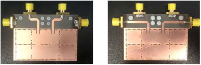
FIGURE 4. The photograph of the fabricated circuit.
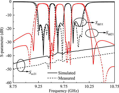
FIGURE 5. Simulated, and measured S-parameters of proposed balanced tri-band BPF.
Comparison of the proposed balanced tri-band BPF with other works is shown in Table 1. It is apparent that our work exhibits many advantages in terms of high selectivity, higher CM suppression and realizes a lower insertion loss.
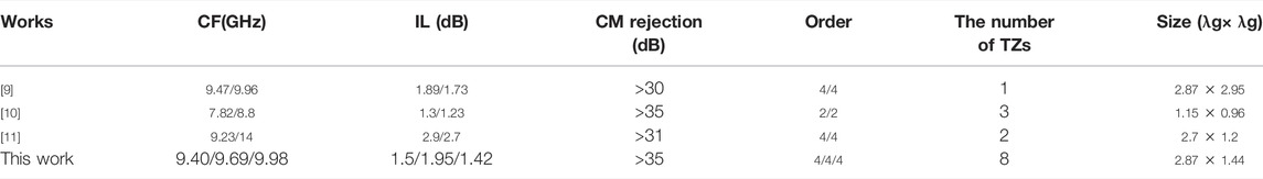
TABLE 1. Comparisons with previous works.
Conclusion
A high selectivity balanced tri-band BPF based on SIW technology has been presented. Results indicate that it presents the function of tri-band DM transmission, integrating high CM suppression and high selectivity. The simulated and measured results have been given with good circuit performance. With all these good properties, we believe the balanced tri-band BPF design can be well implemented for a wide range of micro- and millimeter-wave applications.
Data Availability Statement
The original contributions presented in the study are included in the article/supplementary material, further inquiries can be directed to the corresponding author.
Author Contributions
ML conducted extensive analysis and wrote parts of this paper. MP gave assistance in the measurement and wrote parts of this paper. DW, ZL, and CX revised this paper.
Funding
This work was supported in part by the Natural Science Foundation of the Jiangsu Higher Education Institutions of China, Grant Number: 20KJB510042.
Conflict of Interest
The authors declare that the research was conducted in the absence of any commercial or financial relationships that could be construed as a potential conflict of interest.
Publisher’s Note
All claims expressed in this article are solely those of the authors and do not necessarily represent those of their affiliated organizations, or those of the publisher, the editors and the reviewers. Any product that may be evaluated in this article, or claim that may be made by its manufacturer, is not guaranteed or endorsed by the publisher.
References
1. Shi J, Xue Q. Dual-band and Wide-Stopband Single-Band Balanced Bandpass Filters with High Selectivity and Common-Mode Suppression. IEEE Trans Microwave Theor Techn. (2010) 58(8):2204–12. doi:10.1109/tmtt.2010.2052959
2. Lee C-H, Hsu C-IG, Hsu C-C. Balanced Dual-Band BPF with Stub-Loaded SIRs for Common-Mode Suppression. IEEE Microw Wireless Compon Lett (2010) 20(2):70–2. doi:10.1109/lmwc.2009.2038433
3. Shi J, Xue Q. Balanced Bandpass Filters Using Center-Loaded Half-Wavelength Resonators. IEEE Trans Microwave Theor Techn. (2010) 58(4):970–7. doi:10.1109/tmtt.2010.2042839
4. Dong G, Wang W, Wu Y, Li W, Liu Y, Tentzeris MM. Dual-band Balanced Bandpass Filter Using Slotlines Loaded Patch Resonators with Independently Controllable Bandwidths. IEEE Microw Wireless Compon Lett (2020) 30(7):653–6. doi:10.1109/lmwc.2020.2995963
5. Guo Y-J, Xu K-D, Deng X, Cheng X, Chen Q. Millimeter-wave On-Chip Bandpass Filter Based on Spoof Surface Plasmon Polaritons. IEEE Electron Device Lett (2020) 41(8):1165–8. doi:10.1109/led.2020.3003804
6. Xu K-D, Xia S, Jiang Y, Guo Y-J, Liu Y, Wu R, et al. Compact Millimeter-Wave On-Chip Dual-Band Bandpass Filter in 0.15-μm GaAs Technology. IEEE J Electron Devices Soc (2022) 10:152–6. doi:10.1109/jeds.2022.3143999
7. Xu K-D, Weng X, Li J, Guo Y-J, Wu R, Cui J, et al. 60-GHz Third-Order On-Chip Bandpass Filter Using GaAs pHEMT Technology. Semicond Sci Technol (2022) 37(5):055004. doi:10.1088/1361-6641/ac5bf8
8. Cui Y, Xu K-D, Guo Y-J, Chen Q. Half-mode Substrate Integrated Plasmonic Waveguide for Filter and Diplexer Designs. J Phys D: Appl Phys (2021) 55(12):125104. doi:10.1088/1361-6463/ac44bf
9. Xu X, Wang J, Zhang G, Chen J. Design of Balanced Dual‐band Bandpass Filter Based on Substrate Integrated Waveguide. Electron Lett (2013) 49(20):1278–80. doi:10.1049/el.2013.2371
10. Li P. Balanced Dual-Band SIW Bandpass Filter with Enhanced Selectivity. In: 2020 IEEE MTT-S International Microwave Workshop Series on Advanced Materials and Processes for RF and THz Applications (IMWS-AMP). Suzhou, China (2020). p. 1–3. doi:10.1109/imws-amp49156.2020.9199709
11. Shen Y, Wang H, Kang W, Wu W. Dual-Band SIW Differential Bandpass Filter with Improved Common-Mode Suppression. IEEE Microw Wireless Compon Lett (2015) 25(2):100–2. doi:10.1109/lmwc.2014.2382683
12. Macchiarella G, Tamiazzo S. Design Techniques for Dual-Passband Filters. IEEE Trans Microwave Theor Techn. (2005) 53(11):3265–71. doi:10.1109/tmtt.2005.855749
Keywords: balanced bandpass filter, split topology, tri-band, substrate integrated waveguide, high selectivity
Citation: Min L, Pan M, Wang D, Luo Z and Xu C (2022) A Balanced Tri-Band Substrate Integrated Waveguide Bandpass Filter With High Selectivity. Front. Phys. 10:956745. doi: 10.3389/fphy.2022.956745
Received: 30 May 2022; Accepted: 09 June 2022;
Published: 30 June 2022.
Edited by:
Kai-Da Xu, Xi’an Jiaotong University, ChinaReviewed by:
Yingjiang Guo, University of Electronic Science and Technology of China, ChinaXuedao Wang, Jinling Institute of Technology, China
Copyright © 2022 Min, Pan, Wang, Luo and Xu. This is an open-access article distributed under the terms of the Creative Commons Attribution License (CC BY). The use, distribution or reproduction in other forums is permitted, provided the original author(s) and the copyright owner(s) are credited and that the original publication in this journal is cited, in accordance with accepted academic practice. No use, distribution or reproduction is permitted which does not comply with these terms.
*Correspondence: Congcai Xu, congcaixu_squ@163.com