Analysis and Optimization of Organic Tandem Solar Cells by Full Opto-Electronic Simulation
 Urs Aeberhard1,2*
  Andreas Schiller1,3 Yannick Masson1 Simon J. Zeder1,4 Balthasar Blülle1 Beat Ruhstaller1,3
- 1Fluxim AG, Winterthur, Switzerland
- 2Integrated Systems Laboratory, Department of Information Technology and Electrical Engineering, ETH, Zürich, Switzerland
- 3Institute of Computational Physics, ZHAW, Winterthur, Switzerland
- 4PV-Lab, Institute of Microengineering, EPFL, Neuchâtel, Switzerland
This paper reports on the analysis and optimization of high-efficiency organic tandem solar cells via full opto-electronic device simulation on continuum level and using a hopping model for the explicit description of the charge recombination junction. Inclusion of the electrical sub-cell interconnection allows for a rigorous assessment of the impact of the internal charge distribution and associated built-in fields as well as quasi-Fermi level profiles on the measured device characteristics. It enables the direct evaluation of the external quantum efficiency in a simulation that follows closely the measurement protocol, and sheds light on complications related to the dependence of the band profile on the illumination conditions. The study also points at fingerprints of insufficient junction quality in the electrical characteristics of the tandem device. After studying the impact of key electrical parameters such as, carrier mobility, lifetime and interface hopping rate, onto the device characteristics, the latter are optimized not only optically, but also electronically, adding in both cases an increasing number of layers to the parameters of the global optimization procedure. An improvement of 2% absolute power conversion efficiency by using the full opto-electronic optimization as compared to optical optimization only is found.
1 Introduction
With the demonstration of solar energy conversion efficiencies close to 20% (Wang et al., 2021a), organic photovoltaics (OPV) has recently confirmed its potential for a low cost, flexible and versatile technology for renewable energy supply. These high efficiencies were achieved using a tandem concept, in which two absorber materials with different band gaps are stacked to make better use of the solar spectrum. In fact, due to the prospect of higher conversion efficiencies and larger range of open circuit voltages achievable as compared to single junction technology, multi-junction architectures have become an important focus of organic solar cell research (Ameri et al., 2009; Ameri et al., 2013; Di Carlo Rasi and Janssen, 2019; Zhang et al., 2020). As in the industrially more relevant two-terminal configuration current matching is required to achieve maximum efficiency, the geometry and composition of the complex multi-layer stacks needs to be adjusted carefully. For this task, optical simulations of the absorption within the individual sub-cells were shown to be instrumental (Li et al., 2017; Lingxian et al., 2018; Wang et al., 2021a; Liu et al., 2021). However, small variations in layer thicknesses can have significant impact on charge carrier extraction in low-mobility and defect-rich organic materials, and, hence, on the specifics of the optimum tandem configuration (Tress, 2014). Most importantly, the design of the charge recombination layer connecting the two sub-cells is critical for the performance of the tandem device (Aeberhard et al., 2019; Wang et al., 2021b). The present work intends to assess this impact computationally via full opto-electronic simulation and optimization of the organic tandem solar cell device. To this end, a recently developed interface hopping model describing the charge transfer at the recombination junction (Altazin et al., 2018a) is combined with the standard coupled optical and drift-diffusion-Poisson solvers for organic solar cells, as implemented in the device simulation software Setfos (Fluxim, 2022).
The paper is organized as follows. In Section 2, the physical models and the simulation procedure are briefly reviewed, covering also the approaches for interface hopping and the numerical optimization. In Section 3, the organic tandem solar cell system considered is described in terms of initial geometry and material composition of the layer stack, including a discussion about the extraction of material parameters used. Section 4 provides a detailed discussion of the numerical simulation results, from the analysis of single junction and tandem characteristics—with special focus on the extraction of the tandem external quantum efficiency (EQE)—to the optical and electrical optimization. A brief summary and the main conclusions are given in Section 5.
2 Simulation Approach
The simulations of the organic tandem solar cells are performed using the Setfos tool developed by Fluxim AG, which solves the macroscopic semiconductor transport equations—charge carrier continuity equations with drift-diffusion current coupled to Poisson’s equation for the electrostatic potential (Häusermann et al., 2009; Knapp et al., 2010)—for a quasi-1D problem together with a 1D model for coherent and incoherent light propagation in multi-layer structures based on transfer matrix and net radiation methods (Lanz et al., 2011; Santbergen et al., 2013). Originally developed for the simulation of organic light emitting devices (OLED) (Ruhstaller et al., 2003), Setfos includes advanced mobility models for disordered organic materials, and the physical models implemented have been validated with a broad range of experimental characterization experiments in the fields of OPV (Neukom et al., 2018) and OLED (Jenatsch et al., 2020).
As stated above, the central equations that are solved are the continuity equations for mobile and trapped electron and hole densities n, p, and nt, pt, respectively:
In the above equations, t is the time, z the coordinate along which transport is assumed to proceed, q is the elementary electronic charge, Jn(p) is the electron (hole) current density, is the (optical) volume generation rate, and
where the Einstein relation was used to replace the diffusion constant by the charge carrier mobility µ, and the electric field ℰ is obtained from the solution of Poisson’s equation:
where ε0 is the vacuum permittivity, εr is the relative dielectric constant, and Nacc (Ndon) is the density of ionized acceptor (donor) molecules. In organic semiconductors, the charge carrier mobilities in (5) and (6) may also depend on the local field, in which case a Poole-Frenkel-type expression is used (Frenkel, 1938):
Finally, the charge carrier densities are related via Boltzmann occupation statistics to the effective density of states N0n,p, the HOMO/LUMO energies (including the electrostatic potential profile), and the quasi-Fermi levels EFn,p through,
While Setfos provides solutions of the above equations also in the transient case, the current investigation is restricted to the stationary state, for which any time dependence vanishes. In that case, the trap-mediated inter-band recombination rate for a single defect level at energy Et (measured from the conduction band minimum) with density Nt can be expressed via the Shockley-Read-Hall formalism (Hall, 1952; Shockley and Read, 1952):
where Cn,p are the electron and hole capture rates,
and
Solution of the steady-state drift-diffusion-Poisson problem requires application of appropriate boundary conditions for the charge carrier densities and the electric field. For the latter, the total potential drop over the device thickness L is equated to the difference of applied and built-in potentials,
where the built-in potential is inferred from the top and bottom electrode work functions, qVbi = Φtop − Φbot. For the charge carrier densities, ohmic contacts correspond to a Dirichlet boundary condition defined via the electrode work functions and Exprs. (9) and (10), while thermionic injection is considered using the model of (Scott and Malliaras, 1999) that fixes the injection currents as a (complex) function of carrier mobility, HOMO-LUMO levels, work function, effective density of states, dielectric constant, electric field, and temperature. In order to enable consideration of non-ideal contacts with finite shunt and series resistances RSH and RS, the drift-diffusion model is coupled to an external circuit model containing those resistive elements.
A key feature that enables the electrical simulation of tandem devices with Setfos is the hopping interface model (Altazin et al., 2018b), as it can be used to describe the charge transfer between the monolithically integrated sub-cells. In this model, that is based on the Miller-Abrahams theory of thermally activated hopping in disordered materials (Miller and Abrahams, 1960; Coropceanu et al., 2007), the individual rates for charge transfer can be specified for intra- as well as interband transitions. For the tandem OPV simulations, only HOMO-LUMO transfer is considered, i.e., the junction is assumed to be ideal with respect to leakage currents. The rate of interband hopping connecting the HOMO on the left side with the LUMO on the right side of the interface is then given by (Altazin et al., 2018b)
with
In the above expressions, pr and ar are hole density and molecular lattice spacing of the right side, ν is the attempt frequency of the hopping process (in units of m2s−1), d(x, y) = [(al + ar)2/4 + x2 + y2]1/2 is the hopping distance, γ is the inverse tunneling distance, and ∆El,r is the energy difference between the left and right molecular states involved in the hopping process (see also Figure 1 for an illustration of the hopping model). The associated tunneling particle current density is
where nl and al are now the electron density and molecular lattice spacing on the left side of the interface. Integration into the conventional drift-diffusion-Poisson framework for classical continuum charge transport simulation is then achieved by matching the tunneling current with the drift-diffusion currents on either side of the interface.
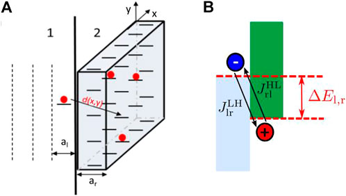
FIGURE 1. Illustration of the charge hopping model implemented in Setfos: (A) Geometrical arrangement of molecular sites and distance of hopping across the interface. (B) Energetic alignment of molecular levels involved in the hopping process.
A further feature of the software Setfos that is used in this work regards the optimization routines. A combination of global and local optimization algorithms is applied to different targets, such as fitting of current-voltage (JV) curves for the extraction of material parameters, and layer thickness optimization of tandem OPV devices for maximum performance based on optical and coupled opto-electronic simulation. For the optical assessment of tandem solar cells, the minimum of the sub-cell photocurrents is maximised. Since the global optimum configuration is achieved in the regime where enhancing the photocurrent in the top cell results in a decrease of the bottom cell current, maximum performance corresponds to the situation of current matching. For the opto-electronic optimization, the photovoltaic power conversion efficiency (PCE) of the tandem device is set directly as the optimization target.
3 Implementation
For the simulation of organic tandem solar cells, we consider the high-efficiency device architecture described in Ref. (Li et al., 2017), consisting of a top cell with a DR3TSBDT:PC71BM absorber layer and a bottom cell based on a DPPEZnP-TBO:PC61BM absorber, connected by a recombination interlayer composed of a combination of ZnO nano-particles and PEDOT:PSS. Thin layers of CuSCN and PFN are used as electron and hole blocking layers at anode and cathode, respectively. The electrodes are formed by ITO and Al. The layer structure and the energy level alignment of the experimental model system used for the simulation are displayed in Figure 2. For the initial layer thicknesses, the values are taken again from Ref. (Li et al., 2017), with the exception of the glass at the top electrode, which is set to 1 mm. Accordingly, the glass substrate is treated as an incoherent layer in the optical simulation. For the electrical simulation, the intrinsic values for HOMO-LUMO levels are taken as indicated in Ref. (Li et al., 2017), and electron and hole transport levels of the individual bulk heterojunctions of the sub-cells are identified as displayed in Figure 2B. The single junction solar cells were implemented following the experimental realization in Ref. (Li et al., 2017), i.e., both absorber materials were sandwiched between PEDOT:PSS as hole transport layer (HTL) and a PFN/Al contact. At the ITO contact, hole injection is modelled via thermionic boundary conditions, while the PFN/Al contact is assumed to be ohmic. For injection of holes into PEDOT:PSS, the ITO work function is set at the standard value of 4.7 eV, while a larger WF of 4.97 eV is used in the case of injection into CuSCN in order to consider the lower effective injection barrier due to the presence of band tails (Kim et al., 2016).
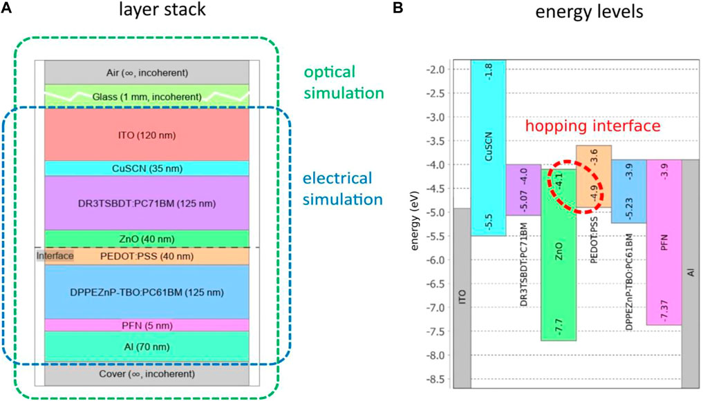
FIGURE 2. (A) Layer stack used for optical and electrical simulations, respectively. (B) Energetic alignment of materials in the electrical device stack. The recombination junction—modelled by the hopping interface—is formed by the ETL of the top cell and the HTL of the bottom cell.
Additionally, a series resistance of 1.2 Ω cm2 is assumed for the top cell in single junction configuration, while a shunt resistance of 1.6 kΩ cm2 is used for all cells.
While the optical material parameters (nk-data) and charge carrier mobilities were taken from the literature 9CuSCN: (Pattanasattayavong et al., 2015; Ezealigo et al., 2020), DR3TSBDT: (Kumari et al., 2017), DPPEZnP-TBO: (Xiao et al., 2017), PFN: (He et al., 2012)], the recombination parameters are adjusted using global multi-parameter optimization routines (dividing rectangles algorithm) to fit the experimental single junction and tandem device characteristics given in (Li et al., 2017). For the tandem simulation, the single junction material parameters are used except for the defect densities in the absorber layers, which are taken as starting values to obtain the defect densities in the tandem configuration. For the effective attempt frequency of the charge hopping at the recombination junction, a value of 𝒱 = 5 × 10⁻⁵ m2/s is chosen. Based on these settings, a good fit of all the JV curves could be achieved with a consistent parameter set, as displayed in Figure 3. All of the optical and electrical parameters used in the simulation of the single junction and tandem devices are given in the Supplementary Material.
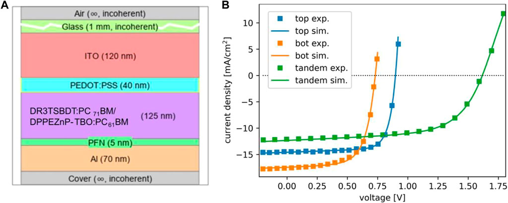
FIGURE 3. (A) Layer stack configuration for modelling of single junction subcells characteristics. (B) Fitting of the experimental single junction sub-cell and tandem current-voltage characteristics (symbols) with the model based on the stacks in (A) and in Figure 2.
The spectrum considered for solar illumination is the ASTM G173-03 (Terrestrial “Global Tilt” AM1.5) reference spectrum from http://rredc.nrel.gov/solar/spectra/am1.5/,which will be referred to as AM1.5G in the following. Due to lack of accurate nk-data for the absorber layers, the generation rate had to be scaled (via ηgen) in order to reproduce the AM1.5G short circuit current given in Ref. (Li et al., 2017) for the reference geometry. For the same reason, the experimental EQE data was not used in the parameter extraction.
4 Numerical Results
4.1 Analysis of Single Junction and Tandem Characteristics
Identification and analysis of electrical losses starts with the comparison of the external quantum efficiency (EQE) with the absorptance. However, the proper determination of the EQE of organic tandem devices is not straightforward, as was realized over a decade ago (Gilot et al., 2010; Gilot et al., 2011). Of course, the main complication—common to all tandem devices—arises from the fact that in order to probe a specific sub-cell, this one needs to be current limiting over the whole range of wavelengths, which requires appropriate bias illumination. For organic devices there is the additional problem that the carrier extraction efficiency depends strongly on the built-in field which, in turn, changes with illumination. This requires the additional application of a bias voltage to establish the conditions found under AM1.5G illumination at global short circuit conditions. Only in this case will the extracted EQE provide the measured short circuit current (JSC) under integration over the AM1.5G flux.
The capability to simulate current flow through the entire device enables us to follow the experimental procedure. This means that we use monochromatic bias light with intensity adjusted to approach AM1.5G generation conditions, such as to establish the appropriate top or bottom limiting situation (i.e., to measure the top-cell EQE we bias the bottom cell and vice versa). Figure 4 shows (a) the extinction coefficients of top and bottom absorbers with the arrows indicating the monochromatic bias illumination at 470 and 700 nm, respectively, and (b) displays the corresponding generation profiles computed by the optical simulation within Setfos, confirming the targeted regime of current limitation.
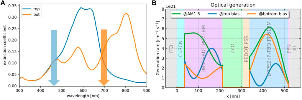
FIGURE 4. Bias illumination applied for the determination of the EQE in the tandem configuration: (A) Sub-cell extinction coefficient and spectral location of the monochromatic bias light. (B) Charge carrier generation profile induced by AM1.5G broadband sunlight and the two monochromatic bias spectra that lead to top or bottom limitation of the photocurrent.
The EQE is then obtained in differential form from the additional current induced by the weak mono- chromatic probe beam. In spite of lacking accurate nk-data in the simulation, there is a rather good agreement with the measured EQE. However, to ensure the internal consistency of the procedure, the short circuit current from the simulation under AM1.5G spectrum is to be compared with the value obtained by integrating the product of EQE and AM1.5G flux over wavelength. Under this spectrum, the tandem device is top limited. We therefore consider the current extracted from the top-cell EQE shown in Figure 5A (dashed lines). The small disagreement of the two currents (12.22 mA/cm2 from EQE vs. 12.19 mA/cm2 from full simulation under AM1.5G flux) is a consequence of the larger reverse top-cell voltage under the 700 nm bias light (Vtop = 0.88 V) as compared to the situation under AM1.5G illumination (Vtop = 0.53 V). This is illustrated in Figures 5B,C that show the band profiles and quasi-Fermi levels for the two illumination conditions and at vanishing applied voltage. If we correct for this difference by application of a corresponding forward bias voltage V = 0.35 V (Figure 5D), the exact same short circuit current is recovered for both EQE (full line in Figure 5A) and full spectrum simulations.
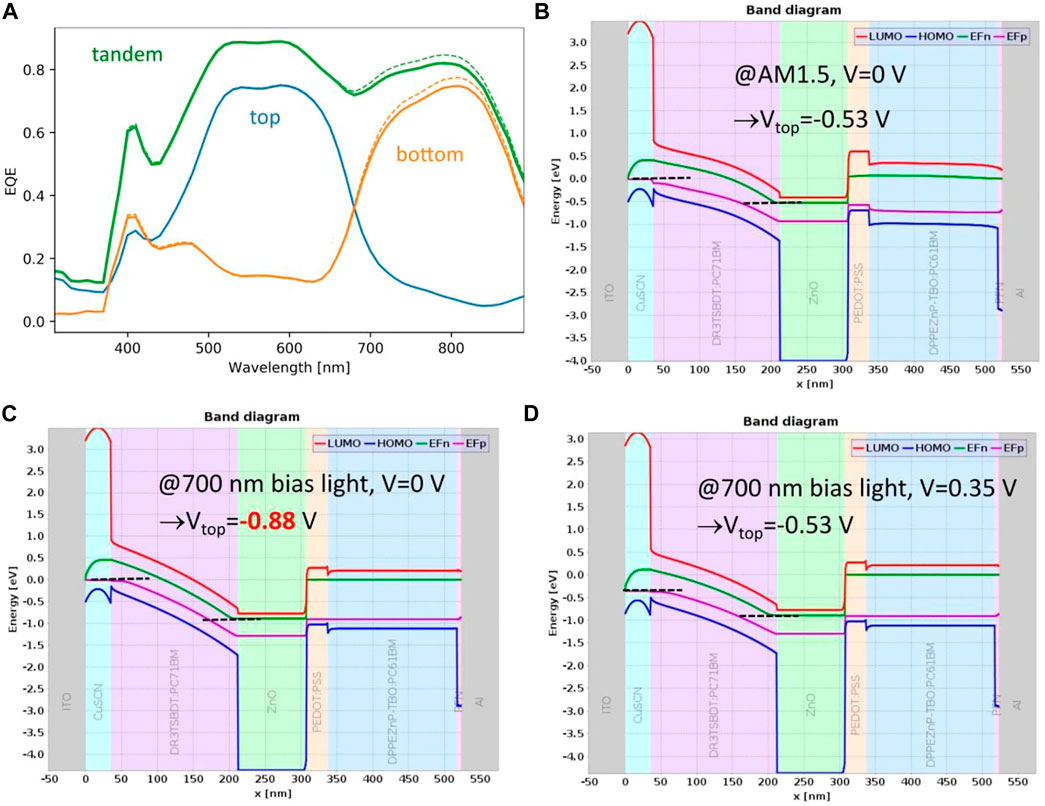
FIGURE 5. (A) Sub-cell EQE from coupled simulations under application of bias light only (dashed lines) and with an additional bias voltage (solid lines). (B) Band profile and quasi-Fermi levels at short circuit conditions (V = 0 V) and under illumination with the AM1.5G spectrum, for which a top-cell voltage of V = 0.53 V develops. (C) Under 700 nm bias light, the top-cell voltage at short circuit conditions amounts to V = 0.88 V. (D) Application of a bias voltage of V = 0.35 V reproduces the AM1.5G short circuit conditions under bias light.
The approach is now ready to be used for the comparison of the EQE with the absorptance. Figure 6 displays the layer-resolved absorptance as a stack plot, overlayed by the bottom/top/tandem EQE curves as yellow dashed/dotted/full lines. Obviously, in the situation considered, carrier extraction is efficient, such that electrical losses are marginal and confined to the long wavelength region. However, this is not obvious from the sub-cell EQEs as extracted from the electrical simulation of the (optically filtered) individual sub-cells (white lines)—an often-used approach (Ding et al., 2011)—which therefore provides only an approximate description of the tandem EQE.
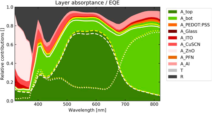
FIGURE 6. Layer-resolved absorptance (parasitic contributions in red) and EQE as obtained from the coupled (yellow) and non-coupled (white) electrical simulations. The contributions of the top and bottom sub-cells are indicated with dashed and dotted lines, respectively. The comparison reveals that the non-coupled simulation underestimates the charge extraction efficiency at short circuit conditions.
To confirm the validity and accuracy of the approach away from the conditions of ideal charge extraction, we consider a device with low bottom cell IQE due to reduced hole mobility and increased SRH recombination—i.e., reduced mobility-lifetime product µτ—in the bottom absorber layer, corresponding to devices exhibiting reduced JSC and fill factor (FF) in their current-voltage characteristics (Figure 7A). In this situation, the tandem becomes bottom limited, which is correctly reflected in the bottom cell EQE (Figure 7B) and in the corresponding short circuit current (Figure 7C), which agree up to numerical inaccuracies. The same applies in a device with low top cell IQE (Figures 7D–F).
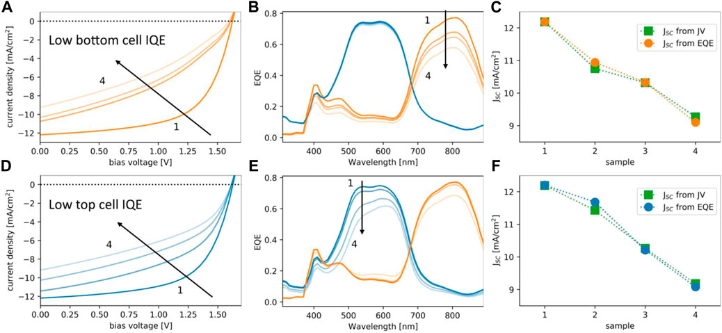
FIGURE 7. Impact on the tandem characteristics of electrical non-idealities at sub-cell level: (A) Current- voltage characteristics for bottom cell IQE from high (sample 1) to low (sample 4). (B) Corresponding evolution of the sub-cell EQE (coupled simulation). (C) Comparison of the tandem JSC as extracted from the EQE or the JV-characteristics, respectively. (D–F): Same for varying top cell IQE.
Since the recombination junction is instrumental for the charge flow in the tandem device, the impact of the charge transfer rate on the EQE is considered next. From the characteristics of the short circuit current vs. hopping rate—shown in Figures 8A two different regimes can be identified: In the large to intermediate hopping rate regime, there is no impact of the rate on JSC. In this situation, the EQE is insensitive to the illumination conditions, as shown in Figure 8C. In the low hopping rate regime, JSC is significantly reduced, and the EQE becomes strongly illumination intensity dependent (Figure 8B), as the current is now limited by the charge transfer rate at the recombination junction.
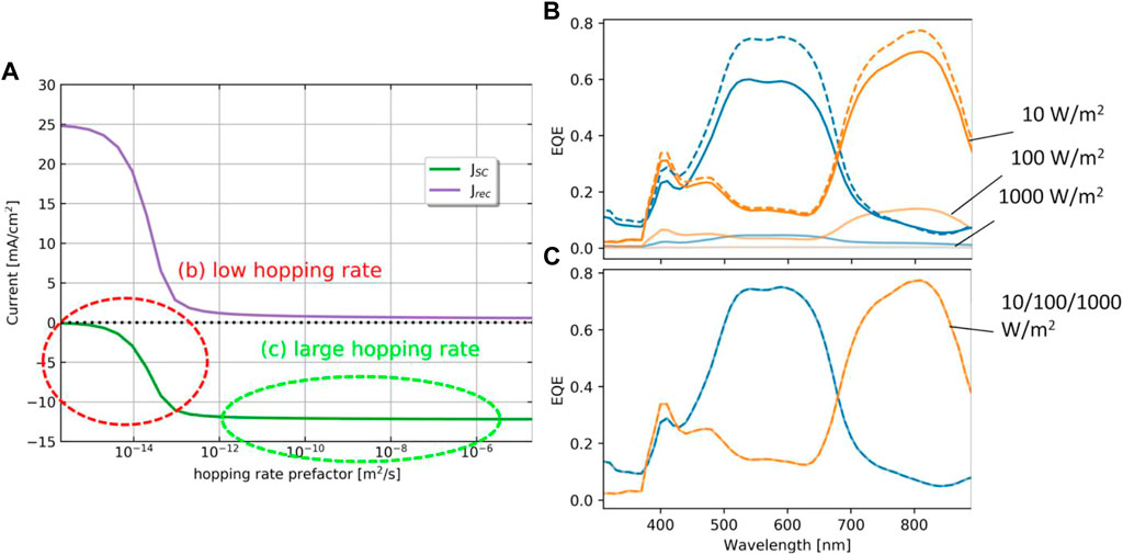
FIGURE 8. Impact on JSC and EQE of the charge transfer rate at the recombination junction: (A) JSC is degraded severely at low hopping rate, while insensitive to the exact value above threshold. (B) In the low hopping rate regime, the EQE is very sensitive to the intensity of the bias illumination, with current being strongly suppressed at high irradiation levels. (C) In the regime of large hopping rates, current is not limited by the rate of charge transfer at the junction, which results in an insensitivity to the illumination level.
While JSC is reduced only in the low hopping rate regime, VOC and FF suffer significant losses already at modest reduction of the hopping rate away from the large hopping regime, as shown in Figure 9A. In fact, there is a threshold value for the hopping rate above which no reduction of VOC can be observed. In that case, one observes a perfect alignment of electron and hole QFLs on either side of the recombination junction, as shown in Figure 9C. Below this threshold, a growing discontinuity in the QFL alignment appears, which corresponds to a junction-related voltage drop that is translated directly into a correspondingly reduced VOC (Figure 9D).
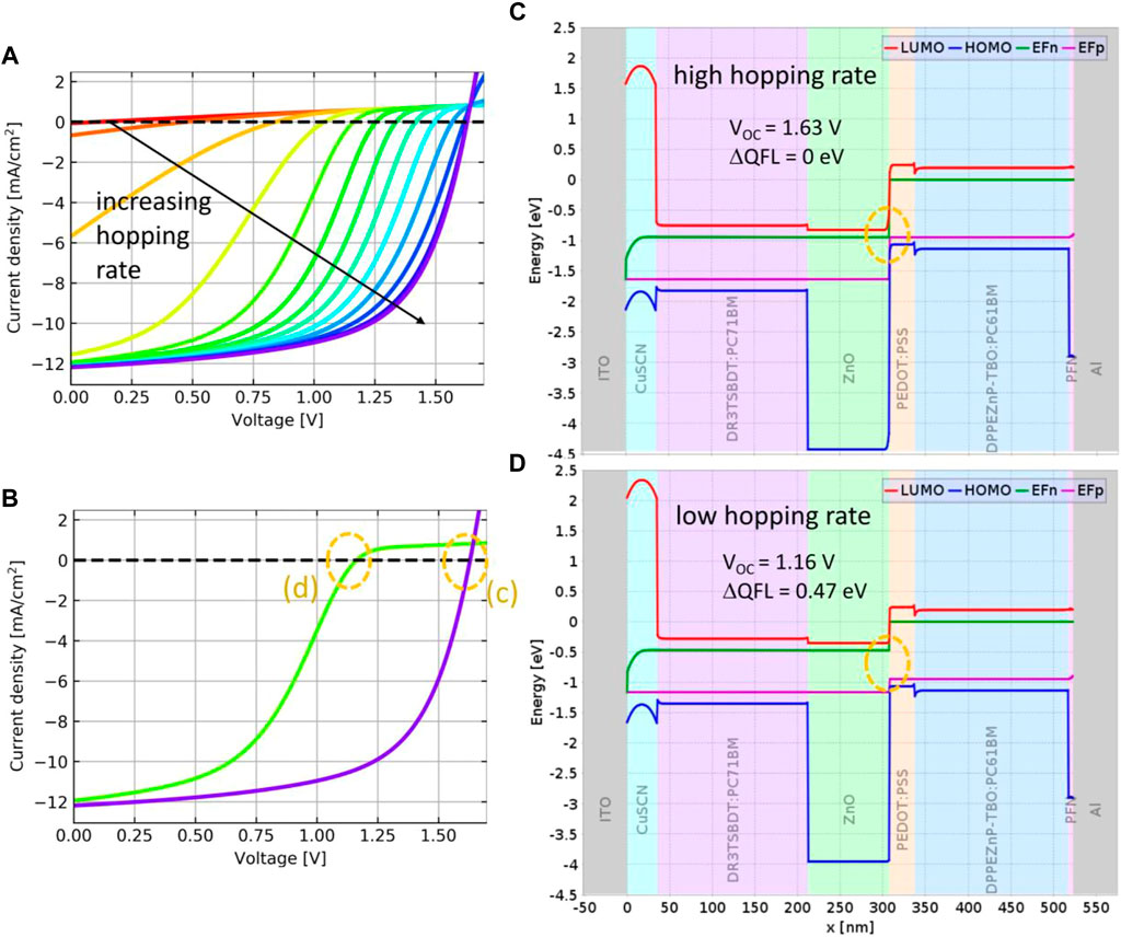
FIGURE 9. Impact on the JV characteristics of the charge carrier hopping rate at the recombination junction: (A) Current-voltage characteristics for attempt frequencies ranging from 2 × 10⁻¹⁶ m2/s to 2 × 10⁻⁴ m2/s. (B) Current voltage characteristics representative for the low (light color) and high (dark color) hopping rate regimes. (C) Band profiles and quasi-Fermi levels at open circuit voltage for the tandem device in the regime of high hopping rate, where the electron and hole QFLs at the junction are perfectly aligned. (D) Band profiles and quasi-Fermi levels at open circuit voltage for the tandem device in the regime of low hopping rate, where a sizable voltage drop originates from the misalignment of the QFLs at the junction.
The availability of the QFL profiles throughout the entire device enables the assessment of the internal voltages Vtop and Vbot of top and bottom sub-cells. As displayed in Figure 10, Vtop is the difference in electron QFL at the internal contact formed by the recombination junction and the hole QFL at the top electrode, while Vbot is the difference between, the electron QFL at the bottom electrode and the hole QFL at the bottom side of the recombination junction. Evaluation of these internal voltages for each value of the external voltage Vapp = Vt applied between top and bottom electrode—and which corresponds to a current density via the tandem characteristics—gives the internal current-voltage characteristics of the sub-cells (dashed lines in Figure 10). These are to be compared to the sub-cell JV curves obtained from the individual electrical simulation of the optically filtered sub-cells (dotted lines), for which the optics of the full stack is considered, and the PEDOT:PSS is used as top-cell bottom electrode and the ZnO as bottom cell top electrode. While the filtered top-cell characteristics underestimates the internal voltage closed to and beyond the sub-cell MPP, it is found that the internal bottom cell voltage obtained from the QFLs is larger than 0.5 V for all values of the external voltage. The graphical construction of the tandem characteristics—which assumes an ohmic internal contact—underestimates VOC in the case of filtered sub-cell characteristics. For the internal JV curves from QFLs, the addition of the curves reproduce VOC correctly, but overestimate the fill factor around MPP. This is consistent with the observation of a finite voltage drop at VMPP in Figure 10A but perfect QFL alignment at VOC as exhibited in Figure 9C. At any rate, the discrepancies between the tandem characteristics obtained from the sub-cell data and the full electrical simulation acquire critical dimensions in the regime of low hopping rates (light solid line).
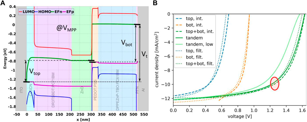
FIGURE 10. (A) Internal voltages Vtop and Vbot as inferred from the QFL profile within the top and bottom sub- cells (shown here at the voltage VMPP of the maximum power point). The terminal voltage Vt corresponds to the difference of the majority carrier QFLs at the external contacts. (B) Comparison of the subcell JV curves obtained from the internal voltages (dashed) with those of the optically filtered sub-cells (dotted). In the case of the filtered cells, the graphical construction of the tandem JV is inaccurate, while the junction-related voltage drop at VMPP is revealed in the difference of the added internal JV curves and the genuine tandem characteristics (solid line).
4.2 Optical and Opto-Electronic Optimization
The most common approach to the optimization of tandem solar cell designs is based on the determination of the minimum of the subcell photocurrents as a function of absorber thickness configuration. For the tandem OPV device under consideration, such a JSC map is shown in Figure 11A. Application of a global optimization algorithm together with the optical simulation correctly identifies the optically ideal absorber thickness combination. Adding an increasing number of device component layers to the multi-parameter optimization routine improves JSC further (Figure 11B).
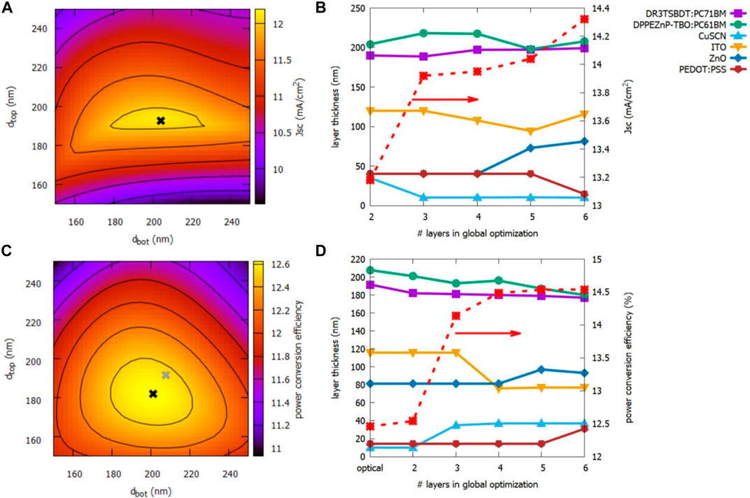
FIGURE 11. Numerical optimization of the tandem OPV layer stack geometry: (A) Short circuit current of the tandem device as a function of top and bottom absorber thicknesses, determined form the optical simulation. The black cross indicates the result of the corresponding numerical optimization routine. (B) Evolution of the short circuit current from optical simulation for subsequent addition of device component layers to the numerical optimization procedure. (C) Power conversion efficiency of the tandem device as a function of top and bottom absorber thicknesses, determined form the fully coupled opto-electronic simulation. The black (grey) cross indicates the result of the global optimization routine using the opto-electronic (optical) simulation. (D) Evolution of the power conversion efficiency from opto-electronic simulation for subsequent addition of device component layers to the numerical optimization procedure.
Eventually, the coupled simulation approach enables the direct optimization of device efficiency under consideration of both, optical and electrical losses. Again, the optimization as restricted to the absorber layers is first compared to the efficiency map as obtained from a brute force sweep over the absorber layer thicknesses. As displayed in Figure 11C, the location of the optimum configuration (black cross) is again identified correctly by the optimization approach. However, the opto-electronically ideal configuration deviates slightly from the optically ideal thickness combination (grey cross). Similar to the optical case, the opto-electronic optimization is then extended to the full layer stack (Figure 11D). While the initial efficiency obtained from the opto-electronic simulation of the optically optimized stack lies only slightly below the one resulting from the opto-electronic optimization, consideration of additional device components leads to an improvement of the conversion efficiency of about 2% absolute. Interestingly, it is not the absorber thicknesses that change most considerably under consideration of electrical aspects, but the contact and charge transport layers. For the latter, improved transport properties overcompensate optical losses at increased layer thicknesses. The ITO front contact adjusts to this new geometry in order to maintain a large optical density in the absorber.
5 Conclusion
We present an approach to the full opto-electronic simulation of organic tandem solar cells that is enabled by the explicit consideration of the charge recombination junction. This provides access to characteristics of the electrically coupled sub-cells such as, external quantum efficiency and internal voltages from quasi-Fermi level profiles under tandem operation, for which prediction based on individual sub-cell characteristics are shown to be prone to inaccuracies. Finally, the coupled approach is demonstrated to allow for device optimization beyond optical considerations, that is, at the maximum power point with the device efficiency as direct target.
Data Availability Statement
The raw data supporting the conclusion of this article will be made available by the authors, without undue reservation.
Author Contributions
AS, YM, SZ, BB, and BR contributed to the development of the numerical simulation software. UA conceptualized the work, performed the simulations, and wrote the manuscript.
Conflict of Interest
UA, AS, YM, SZ, BB, and BR were employed by Fluxim AG.
Publisher’s Note
All claims expressed in this article are solely those of the authors and do not necessarily represent those of their affiliated organizations, or those of the publisher, the editors and the reviewers. Any product that may be evaluated in this article, or claim that may be made by its manufacturer, is not guaranteed or endorsed by the publisher.
Acknowledgments
The authors thank Sandra Jenatsch and Simon Züfle from Fluxim for valuable discussions.
Supplementary Material
The Supplementary Material for this article can be found online at: https://www.frontiersin.org/articles/10.3389/fphot.2022.891565/full#supplementary-material
References
Aeberhard, U., Altazin, S., Stepanova, L., Stous, A., Blulle, B., Kirsch, C., et al. (2019). “Numerical Optimization of Organic and Hybrid Multijunction Solar Cells,” in 2019 IEEE 46th Photovoltaic Specialists Conference (PVSC), 0105–0111. doi:10.1109/PVSC40753.2019.8980824
Altazin, S., Kirsch, C., Knapp, E., Stous, A., and Ruhstaller, B. (2018). Refined Drift-Diffusion Model for the Simulation of Charge Transport across Layer Interfaces in Organic Semiconductor Devices. J. Appl. Phys. 124, 135501. doi:10.1063/1.5043245
Altazin, S., Stepanova, L., Werner, J., Niesen, B., Ballif, C., and Ruhstaller, B. (2018). Design of Perovskite/crystalline-Silicon Monolithic Tandem Solar Cells. Opt. Express 26, A579–A590. doi:10.1364/oe.26.00a579
Ameri, T., Dennler, G., Lungenschmied, C., and Brabec, C. J. (2009). Organic Tandem Solar Cells: A Review. Energy Environ. Sci. 2, 347–363. doi:10.1039/B817952B
Ameri, T., Li, N., and Brabec, C. J. (2013). Highly Efficient Organic Tandem Solar Cells: a Follow up Review. Energy Environ. Sci. 6, 2390–2413. doi:10.1039/C3EE40388B
Coropceanu, V., Cornil, J., da Silva Filho, D. A., Olivier, Y., Silbey, R., and Brédas, J.-L. (2007). Charge Transport in Organic Semiconductors. Chem. Rev. 107, 926–952. doi:10.1021/cr050140x
Di Carlo Rasi, D., and Janssen, R. A. J. (2019). Advances in Solution-Processed Multijunction Organic Solar Cells. Adv. Mat. 31, 1806499. doi:10.1002/adma.201806499
Ding, K., Kirchartz, T., Pieters, B. E., Ulbrich, C., Ermes, A. M., Schicho, S., et al. (2011). Characterization and Simulation of a-Si:H/μc-Si:H Tandem Solar Cells. Sol. Energy Mater. Sol. Cells 95, 3318–3327. doi:10.1016/j.solmat.2011.07.023
Ezealigo, B. N., Nwanya, A. C., Simo, A., Bucher, R., Osuji, R. U., Maaza, M., et al. (2020). A Study on Solution Deposited CuSCN Thin Films: Structural, Electrochemical, Optical Properties. Arabian J. Chem. 13, 346–356. doi:10.1016/j.arabjc.2017.04.013
Fluxim, A. G. (2022). Setfos v5.2. Available at: https://www.fluxim.com/setfos.
Frenkel, J. (1938). On Pre-breakdown Phenomena in Insulators and Electronic Semi-conductors. Phys. Rev. 54, 647–648. doi:10.1103/PhysRev.54.647
Gilot, J., Wienk, M. M., and Janssen, R. A. J. (2011). Measuring the Current Density - Voltage Characteristics of Individual Subcells in Two-Terminal Polymer Tandem Solar Cells. Org. Electron. 12, 660–665. doi:10.1016/j.orgel.2011.01.014
Gilot, J., Wienk, M. M., and Janssen, R. A. J. (2010). Measuring the External Quantum Efficiency of Two-Terminal Polymer Tandem Solar Cells. Adv. Funct. Mat. 20, 3904–3911. doi:10.1002/adfm.201001167
Hall, R. N. (1952). Electron-hole Recombination in Germanium. Phys. Rev. 87, 387. doi:10.1103/physrev.87.387
Häusermann, R., Knapp, E., Moos, M., Reinke, N. A., Flatz, T., and Ruhstaller, B. (2009). Coupled Optoelectronic Simulation of Organic Bulk-Heterojunction Solar Cells: Parameter Extraction and Sensitivity Analysis. J. Appl. Phys. 106, 104507. doi:10.1063/1.3259367
He, Z., Zhong, C., Su, S., Xu, M., Wu, H., and Cao, Y. (2012). Enhanced Power-Conversion Efficiency in Polymer Solar Cells Using an Inverted Device Structure. Nat. Phot. 6, 591–595. doi:10.1038/nphoton.2012.190
Jenatsch, S., Züfle, S., Blülle, B., and Ruhstaller, B. (2020). Combining Steady-State with Frequency and Time Domain Data to Quantitatively Analyze Charge Transport in Organic Light-Emitting Diodes. J. Appl. Phys. 127, 031102. doi:10.1063/1.5132599
Kim, M., Park, S., Jeong, J., Shin, D., Kim, J., Ryu, S. H., et al. (2016). Band-tail Transport of Cuscn: Origin of Hole Extraction Enhancement in Organic Photovoltaics. J. Phys. Chem. Lett. 7, 2856–2861. doi:10.1021/acs.jpclett.6b01039
Knapp, E., Häusermann, R., Schwarzenbach, H. U., and Ruhstaller, B. (2010). Numerical Simulation of Charge Transport in Disordered Organic Semiconductor Devices. J. Appl. Phys. 108, 054504. doi:10.1063/1.3475505
Kumari, T., Lee, S. M., Kang, S. H., Chen, S., and Yang, C. (2017). Ternary Solar Cells with a Mixed Face-On and Edge-On Orientation Enable an Unprecedented Efficiency of 12.1%. Energy Environ. Sci. 10, 258–265. doi:10.1039/C6EE02851A
Lanz, T., Ruhstaller, B., Battaglia, C., and Ballif, C. (2011). Extended Light Scattering Model Incorporating Coherence for Thin-Film Silicon Solar Cells. J. Appl. Phys. 110, 033111. doi:10.1063/1.3622328
Li, M., Gao, K., Wan, X., Zhang, Q., Kan, B., Xia, R., et al. (2017). Solution-processed Organic Tandem Solar Cells with Power Conversion Efficiencies >12. Nat. Photonics 11, 85–90. doi:10.1038/nphoton.2016.240
Lingxian, M., Yamin, Z., Xiangjian, W., Chenxi, L., Xin, Z., Yanbo, W., et al. (2018). Organic and Solution-Processed Tandem Solar Cells with 17.3% Efficiency. Science 361, 1094–1098. doi:10.1126/science.aat2612
Liu, G., Xia, R., Huang, Q., Zhang, K., Hu, Z., Jia, T., et al. (2021). Tandem Organic Solar Cells with 18.7% Efficiency Enabled by Suppressing the Charge Recombination in Front Sub-cell. Adv. Funct. Mat. 31, 2103283. doi:10.1002/adfm.202103283
Miller, A., and Abrahams, E. (1960). Impurity Conduction at Low Concentrations. Phys. Rev. 120, 745–755. doi:10.1103/PhysRev.120.745
Neukom, M., Züfle, S., Jenatsch, S., and Ruhstaller, B. (2018). Opto-electronic Characterization of Third-Generation Solar Cells. Sci. Technol. Adv. Mater. 19, 291–316. doi:10.1080/14686996.2018.1442091
Pattanasattayavong, P., Mottram, A. D., Yan, F., and Anthopoulos, T. D. (2015). Study of the Hole Transport Processes in Solution-Processed Layers of the Wide Bandgap Semiconductor Copper(I) Thiocyanate (CuSCN). Adv. Funct. Mat. 25, 6802–6813. doi:10.1002/adfm.201502953
Ruhstaller, B., Beierlein, T., Riel, H., Karg, S., Scott, J. C., and Riess, W. (2003). Simulating Electronic and Optical Processes in Multilayer Organic Light-Emitting Devices. IEEE J. Sel. Top. Quantum Electron. 9, 723–731. doi:10.1109/JSTQE.2003.818852
Santbergen, R., Smets, A. H. M., and Zeman, M. (2013). Optical Model for Multilayer Structures with Coherent, Partly Coherent and Incoherent Layers. Opt. Express 21, A262–A267. doi:10.1364/OE.21.00A262
Scott, J. C., and Malliaras, G. G. (1999). Charge Injection and Recombination at the Metal-Organic Interface. Chem. Phys. Lett. 299, 115–119. doi:10.1016/S0009-2614(98)01277-9
Shockley, W., and Read, W. T. (1952). Statistics of the Recombinations of Holes and Electrons. Phys. Rev. 87, 835–842. doi:10.1103/physrev.87.835
Tress, W. (2014). Organic Solar Cells: Theory, Experiment, and Device Simulation. Springer International Publishing.
Wang, J., Zheng, Z., Zu, Y., Wang, Y., Liu, X., Zhang, S., et al. (2021). A Tandem Organic Photovoltaic Cell with 19.6% Efficiency Enabled by Light Distribution Control. Adv. Mat. 33, 2102787. doi:10.1002/adma.202102787
Wang, P., Li, W., Sandberg, O. J., Guo, C., Sun, R., Wang, H., et al. (2021). Tuning of the Interconnecting Layer for Monolithic Perovskite/organic Tandem Solar Cells with Record Efficiency Exceeding 21%. Nano Lett. 21. doi:10.1021/acs.nanolett.1c02897
Xiao, L., Liang, T., Gao, K., Lai, T., Chen, X., Liu, F., et al. (2017). Ternary Solar Cells Based on Two Small Molecule Donors with Same Conjugated Backbone: The Role of Good Miscibility and Hole Relay Process. ACS Appl. Mat. Interfaces 9, 29917–29923. doi:10.1021/acsami.7b07960
Keywords: organic photovoltaics (OPV), tandem solar cell, simulation, numerical optimization, drift-diffusion
Citation: Aeberhard U, Schiller A, Masson Y, Zeder SJ, Blülle B and Ruhstaller B (2022) Analysis and Optimization of Organic Tandem Solar Cells by Full Opto-Electronic Simulation. Front. Photonics 3:891565. doi: 10.3389/fphot.2022.891565
Received: 07 March 2022; Accepted: 19 April 2022;
Published: 20 October 2022.
Edited by:
Rudi Santbergen, Delft University of Technology, NetherlandsCopyright © 2022 Aeberhard, Schiller, Masson, Zeder, Blülle and Ruhstaller. This is an open-access article distributed under the terms of the Creative Commons Attribution License (CC BY). The use, distribution or reproduction in other forums is permitted, provided the original author(s) and the copyright owner(s) are credited and that the original publication in this journal is cited, in accordance with accepted academic practice. No use, distribution or reproduction is permitted which does not comply with these terms.
*Correspondence: Urs Aeberhard, urs.aeberhard@fluxim.com