Electron conduction mechanism in indium oxide and its implications for amorphous transport
 Yaoqiao Hu
  Kyeongjae Cho*
- Department of Materials Science and Engineering, The University of Texas at Dallas, Richardson, TX, United States
The electron conduction mechanism in indium oxide (In2O3) and its implications for amorphous transport have been investigated from an orbital overlap perspective. Combined density functional theory and empirical tight binding modeling reveal that the electron transport is facilitated by the neighboring metal atomic s orbital overlap “without” oxygen’s p-orbital involvement. In other words, the electron transport pathway in oxides is only due to the metal-metal medium range connection. This electron conduction mechanism is extended to amorphous In2O3 which unveils that the amorphous disorder influences the electron transport through impacting the metal-metal medium range order including metal-metal coordination number and metal-metal separation. Our results provide an insight into the current theoretical understanding of electron transport in amorphous oxide semiconductors.
1 Introduction
Oxide semiconductors (e.g., ZnO, SnO2, In2O3, Ga2O3, and InGaZnO) have been widely used for thin film transistors and transparent conducting electrodes for decades due to their high phase stability, easy of synthesis at low temperature, wide bandgap, and high carrier mobility. (Nomura et al., 2003; Fortunato et al., 2012; Park et al., 2012; Troughton and Atkinson, 2019; Lee, 2020; Shi et al., 2021). More recently, oxide semiconductors, especially In2O3, have also found their applications as channel materials for back-end-of-line (BEOL) transistors in realizing vertical CMOS technology. (Salahuddin et al., 2018; Hu et al., 2019; Chakraborty et al., 2020; Hu et al., 2020; Si et al., 2020; Si et al., 2021). Oxide semiconductors are typically present in amorphous phase due to their low synthesis temperatures. (Park et al., 2012; Troughton and Atkinson, 2019; Lee, 2020). Understanding the electron transport in amorphous phase oxides would be valuable for tailoring materials properties for the purpose of high-performance electronic device applications.
As the oxide semiconductors are present in thin films, various factors that could influence the electron transport in amorphous oxide semiconductors. It is well known that the oxygen vacancy is ubiquitous in oxides and oxygen vacancies are the sources of electron doping in oxides (Ide et al., 2019; Shi et al., 2021). Film density, which determines the atomic packing density at microscale, is also reported to influence the electron mobility (Ide et al., 2019). Interestingly, Buchholz et al. (Buchholz et al., 2014) have reported a strong dependence of electron mobility on In2O3 film crystallinity where the mobility reaches its maximum value at an intermediate degree of nanocrystalline. Other factors, such as interface and surface have been also mentioned influencing the carrier generation and electron transport in the literature (Shi et al., 2021).
Current understanding on the electron transport mechanism in amorphous oxide semiconductors is based on Hosono’s proposed idea which has been widely accepted in the literature (Takagi et al., 2005; Robertson, 2008; Walsh et al., 2011): the electron conduction pathway (ECP) is due to the orbital overlap between extended s orbitals of neighboring metal atoms. This ECP, because of spherical symmetry of s orbital, is immune from local structural distortion present in amorphous phase so that amorphous oxide semiconductors exhibit high electron mobility comparable to the crystalline phase. This concept also explains well the low electron mobility in amorphous Si where ECP is composed of directional sp (Park et al., 2012)-orbital overlaps which can be easily altered by local structure distortion such as bonding angle variation.
The structures of amorphous oxide semiconductors have been investigated mainly from theoretical modeling approaches. Walsh et al. (Walsh et al., 2009) reported that the amorphous oxide phases are defined by the random packing of cation centered polyhedra, where the local metal-oxygen coordination motifs are largely preserved but the long-range packing of these polyhedra is disordered. Later, Buchholz et al. (Buchholz et al., 2014) systematically studied the structural properties of amorphous In2O3 (a-In2O3) and revealed that long-range order loss is resulted from the InOx polyhedra random rotation around each other. The random polyhedra packing model is a significant advancement towards the understanding of the structure of amorphous oxide semiconductors.
In this work, we devote to investigating the electron transport mechanisms in In2O3 and its implication for amorphous phase electron transport. We base our study on an orbital overlap perspective: the orbital overlap enables electron transport and the continuous orbital overlaps of the involved atomic pair form the ECP. The ECP gives information of how amorphous disorders would influence the electron transport in amorphous phases. Our analysis includes atomic structure characterization, first principles density functional theory (DFT) calculations, and empirically tight binding (ETB) modeling, under which the orbital pair contribution to ECP, i.e., the microscopic electron conduction mechanism, is revealed. Our results provide an important contribution to the current understanding of electron transport mechanism in In2O3 and practical guidance on tailoring In2O3 properties for high-performance In2O3 based electronic devices.
2 Computational methods
2.1 DFT calculation
First principles DFT calculations were performed using Vienna ab initio simulation package (VASP). (Kresse and Hafner, 1994; Kresse and Furthmüller, 1996). Projector-augmented-wave (PAW) (Blöchl, 1994) and pseudopotential methods were used. Generalized gradient approximation of Perdew–Burke–Ernzerhof (GGA-PBE) formalism functional was used for electronic exchange-correlation description. (Perdew et al., 1992; Perdew et al., 1996). For all calculations, an energy cutoff of 420 eV was adopted for the plane-wave basis expansion. Electronic structures including band structure and density of states were calculated using Davidson-block minimization scheme with convergence criteria being energy difference less than 10–5 eV between two adjacent iterations. Brillouin zone sampling grid density varies according to the primitive cell size with an absolute density no less than 0.03Å-1. To accommodate the underestimation of band gap by DFT, band edges were rigidly shifted to reproduce the experimental band gaps.
2.2 Empirical tight binding model
ETB analysis of band structures was following Harisson’s model. (Harrison, 2012). The cutoff radius for orbital overlap interaction is 5Å which includes nearest neighboring, second nearest neighboring, and third nearest neighboring atomic orbital overlap. Orbital overlap strength decays with distance according to V = ηħ2/(md2) where η is orbital-dependent overlap strength and d is the interatomic distance. In our TB mode, four types of orbital overlap are considered: ssσ (metal-s/metal-s), spσ (metal-s/O-p), ppσ (O-p/O-p), and ppπ (O-p/O-p). Initially starting with the parameters given by Harisson for on-site atomic orbital energies and orbital overlap strengths, we semi-empirically fitted the parameters until the TB band structure reproduces the conduction band features of DFT data. ETB parameters used in this work: indium s-orbital on-site energy E (In-s) = −5.0 eV, oxygen p-orbital E (O-p) = −14.1 eV, orbital overlap integrals η (ssσ) = −0.60, η (spσ) = 0.27, η (ppσ) = 0.79, η (ppπ) = −0.21. For simplicity, only s orbitals of metal atoms and p orbitals of oxygen are included in our tight binding model. Comparison of DFT and ETB band structures of In2O3 is shown in Figure 2 in this paper.
2.3 Amorphous phase modeling
The atomic structure of amorphous phase In2O3 was generated by simulating the melt-quench process using ab initio molecular dynamics (AIMD) modeling. (Buchholz et al., 2014; Hu et al., 2023a; Hu et al., 2023b). In the melt step, a large In2O3 crystalline supercell (230 atoms, 15.0 Å × 15.0 Å × 15.0Å) was heated at 3000K for 6ps to obtain amorphous liquid phase. The amorphous liquid phase was then subjected to cooling process at a quenching rate of 200K/ps, followed by a thermal annealing at 300K for 2ps. To make this time-consuming AIMD feasible, a low cutoff energy of 250eV and single Γ-point k-space sampling were used. The obtained melt-quench phase was later geometrically relaxed to its local energy-minimum state by standard DFT modeling. Five independent a-In2O3 atomic structures were generated by repeating the melt-quench process 5 times. Finally, a typical a-In2O3 structure which is not significantly different from other four amorphous structures was selected for structure and electron transport analysis.
3 Results and discussion
Crystalline In2O3 (c-In2O3) assumes the cubic (bixbyite type) crystal structure (Ia3, # 206). The lattice constant for bixbyite c-In2O3 unit cell is a = 10.1Å. The primitive cell of c-In2O3 is shown in Figure 1A. According to Pauling’s rule and other reference works (Pauling, 1929; Walsh et al., 2009; Buchholz et al., 2014), for a typical metal oxide which is an ionic compound, its crystal structure can be viewed as regular packing of MOx polyhedron (Figure 1B). At short-range order (SRO, defined as the metal-oxygen nearest neighboring bonding), each metal cation is surrounded by coordinated oxygen anion forming polyhedron. The polyhedra are then connected together by sharing common oxygen atoms either at the polyhedral corner (corner sharing), or at the edge (edge sharing), or at the face (face sharing). The medium-range order (MRO) is defined as metal-metal second nearest neighboring bonding. MRO is essentially the metal-metal connectivity and is determined by the common oxygen atom sharing. In In2O3, each In atom is coordinated to 6 O atoms forming an octahedron, and different octahedra are linked together by sharing either corner or edge. Each In, in terms of MRO, is coordinated to 12 In atoms, of which 6 are corner sharing (In-In corner) and six are edge sharing (in-In edge). Figure 1C illustrates these two types of In-In coordination: In-In corner where two In atoms share only one common oxygen atom, and In-In edge where two In atoms share two common oxygen atoms.

Figure 1. Atomic structure of In2O3. (A) Primitive cell of bixbyite type In2O3. (B) Polyhedron viewpoint of In2O3 crystal structure. (C) Illustration of corner sharing and edge sharing.
The band structure of c-In2O3 is presented in Figure 2A c-In2O3 has a wide band gap of ∼ 3eV due to the large electronegativity difference between oxygen and indium. In terms of band edge features, a strongly dispersive bottom conduction band can be observed with large contribution from indium s-orbitals and lesser contribution from O-2p orbitals. The much flatter top valence band is almost solely dominated by O-2p orbitals. As a result, In2O3 has a small electron effective mass and a large hole effective mass. The dispersion polarity between conduction band and valence band can be explained by atomic orbital characters. From tight binding point of view, the band dispersion is due to the atomic orbital overlap and a stronger interatomic orbital overlap leads to a stronger band dispersion. Indium s orbitals are more delocalized and spatially more spreading out with larger orbital radii. As a result, stronger overlap is expected between neighboring metal’s s-orbitals. In comparison, O-2p orbital is more localized and directional with smaller orbital radius leading to weaker p-orbital overlap between neighboring O atoms.
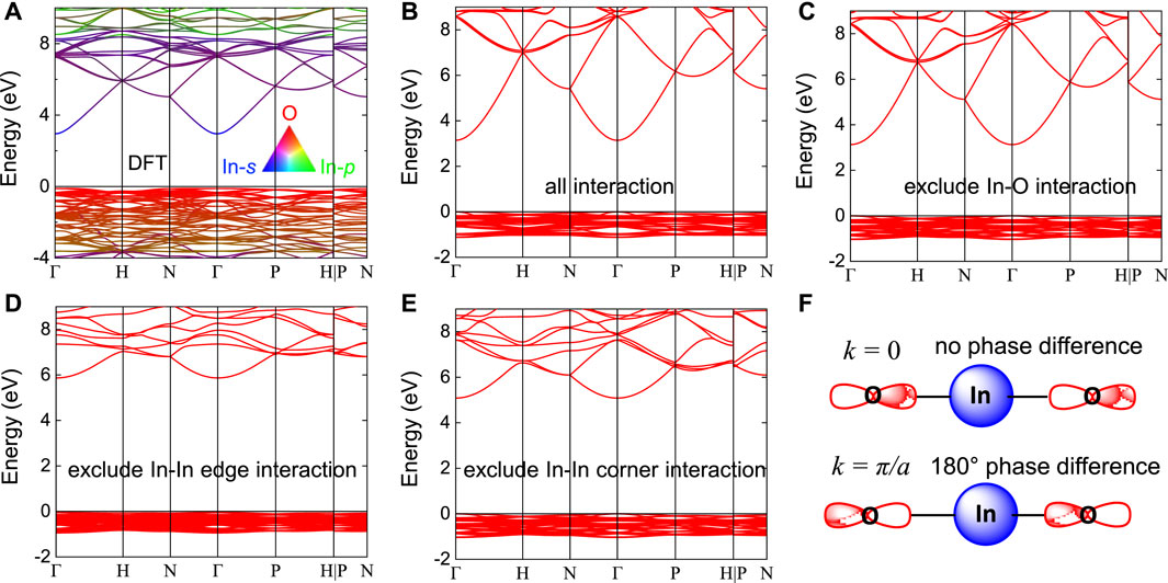
Figure 2. ETB analysis on band dispersion contribution and the derived electron conduction pathway. (A) band structures of In2O3. The band structure is computed using DFT-PBE potential. The band gap was reproduced by rigidly upshifting the conduction band. A color scheme is used to visualize the atomic orbital contribution to each band. (B–E) Band structure of In2O3 calculated using the following assumptions: (B) all orbital overlap interactions included, (C) no orbital interaction between In and O atoms, (D) no orbital interaction between In atoms edge sharing connected, and (E) no orbital interaction between In atoms corner sharing connected. (F) Schematics showing the In-O orbital overlap interaction in In2O3 at k = 0 bonding state and k = π/a antibonding state.
The electron transport is a key property for metals oxides used as transparent conducting oxides and semiconducting channel materials. Drude model states that the carrier mobility depends on the effective mass through μ = eτ/m*, where e is the elementary charge and τ is the electron momentum relaxation time. This expression indicates that electron mobility is determined by the band dispersion since the effective mass is simply the band dispersion curvature. Since the band dispersion is due to the interatomic orbital overlap, stronger orbital overlap interaction would therefore lead to smaller effective mass and higher electron mobility. Microscopically, electron transport is achieved by electron delocalization movement facilitated by orbital overlap. The continuous atomic overlap throughout the entire crystal thus forms the ECP. For In2O3, the conduction band is dominated by metal’s s-orbital and lesser contribution from O-2p orbital. It is thus expected that two types of orbital overlap, metal-s/metal-s direct orbital overlap and metal-s/O-2p/metal-s indirect orbital overlap, could form the ECP.
To resolve the contribution from each type of orbital overlap and to determine the ECP in In2O3, we have performed tight binding analysis on the band structure of In2O3. In tight binding model, individual orbital overlap interaction can be arbitrarily included or excluded, and their effect on the band dispersion can be examined. This directly provides us a way to determine whether a specific orbital overlap contributes to the band dispersion and eventually electron transport. Figure 2 shows the ETB model of In2O3 band structure, with orbital overlap integral empirical parameters fitted to reproduce the DFT band structure. It can be seen that the band dispersion features, especially the bottom conduction band, agree well with the DFT result. Band structures were then calculated based on the following assumptions: (a) all interactions between all atom pairs, (b) In-O orbital overlap interaction excluded, (c) In-In edge interaction excluded, and (d) In-In corner interaction excluded. It is found that when In-O orbital overlap interaction is excluded, the conduction band is identical to that of all interactions included. This suggests that In-O orbital overlap interaction does not contribute to the conduction band dispersion. Therefore, In-O-In indirect orbital overlap behaves as if it is not involved in electron transport and only In-s/In-s direct orbital overlap forms the ECP. The observation that In-O orbital overlap interaction does not contribute to the conduction band dispersion can be explained by the orbital symmetry. In-s orbital presents a spherical symmetry while O-2p orbital has two lobes antisymmetric with respect to the atomic center (Figure 2F). When neighboring atomic orbitals overlap, each O will form a pair of In-s/O-p bonding interaction from one lobe but simultaneously another pair of In-s/O-p antibonding interaction from the other lobe. The bonding and antibonding interaction around O-p completely cancel each other and O atoms always present a zero net orbital interaction with neighboring In atoms. As a result, In-O orbital interaction does not contribute to the E-k dispersion. We thus conclude that in In2O3 metal-s/O-p/metal-s indirect overlap does not contribute to the electron transport in metal oxides and only metal-s/metal-s direct orbital overlap forms the ECP.
This above result is in contrast to the traditional understanding that in metal oxides the conduction band dispersion is mainly facilitated by the metal’s s-orbital overlap with lesser contribution from oxygen p-orbital. As mentioned in the Introduction part, electron conduction is due to the orbital overlap between extended s orbitals of neighboring metal atoms. Our results suggest that the electron transport is “entirely” facilitated by metal’s s-orbital “without” oxygen p-orbital involvement. Our results support Hosono’s model that electron conduction is due to the orbital overlap between metal atoms. Our work further develops this model that metal-metal medium range connection is the determining factor to the electron transport. Note that O-p orbitals are still contributing to the band structure including the valence bands. Oxygen atoms also maintain the lattice charge neutrality and their p-orbitals alternate with indium s-orbitals to ensure orbital stability.
It would be instructive to characterize the amorphous phase atomic structure before diving into the electron transport in amorphous oxides. Upon amorphization, InOx polyhedra will be distorted through O-In-O bond angle and In-O bond length variation. Amorphous phases retain SRO to a large degree in a sense that the local bonding (InOx polyhedra) is only minorly distorted. SRO is largely maintained in amorphous oxides due to the strong chemical bonding between metal and oxygen atoms. No homopolar bonds are expected for amorphous metal oxides (see radial distribution function of In2O3 in Figure 3A). In terms of MRO, a viewpoint on amorphous structure is that MOx polyhedra in amorphous are connected in a distorted way, contrasting to regular packing in crystalline phase. (Buchholz et al., 2014). Such distortion can be viewed as one MOx polyhedron being rotated relative another MOx polyhedron. Figure 3 illustrates this concept using the In2O3 structure. The net effect from polyhedra rotation is that In-In medium range connections are distorted. In In2O3, the metal-metal medium-range connections are critical to electron transport; therefore, the amorphous disorder influence on electron transport could be revealed from metal-metal MRO. “Polyhedra rotation” in amorphous phases also results in short-range disorder including In-O bonding distance and coordination number change. Figures 3C,D show that when InOx rotated, two neighboring InOx polyhedra change from edge sharing to corner sharing which results in In coordination number reduction. This result is consistent with previous work by Buchholz et al. (Buchholz et al., 2014) Figure 3B presents the distribution of the coordination numbers (CN) of In and O atoms. The average CN of In and O are 5.5 and 3.7, respectively, in comparison with six and four in c-In2O3. The “polyhedron rotation” in amorphous phase results in certain amount of loss of MRO, which gradually leads to the complete loss of long-range order.
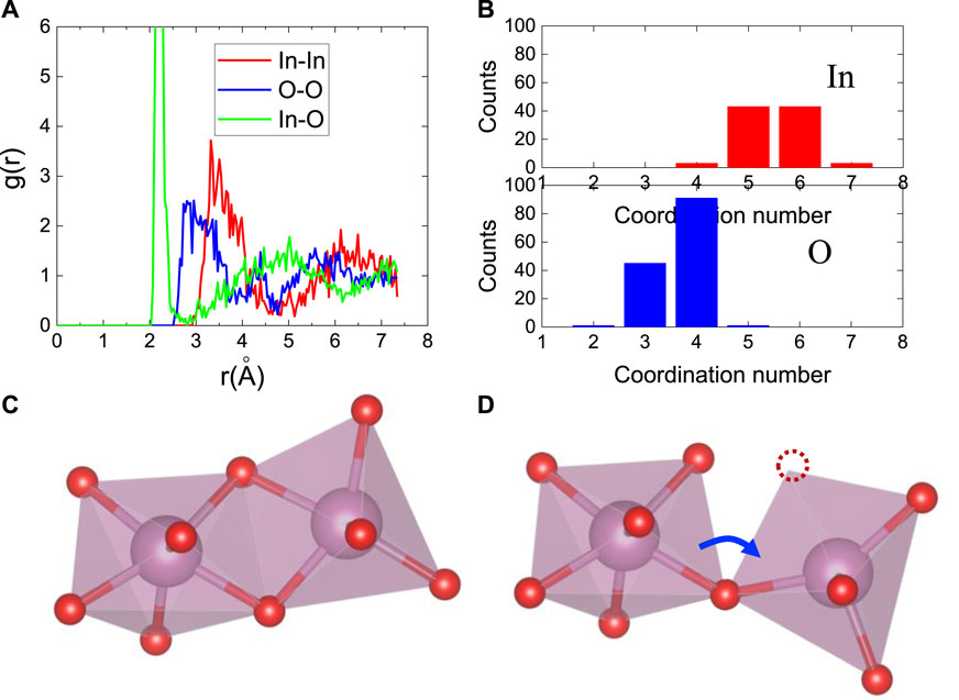
Figure 3. Amorphous structure characteristics using a-In2O3 as an example. (A) Radial distribution function of a-In2O3: In-In pair, In-O pair, and O-O pair. (B) The statistical distribution of In an O coordination number. (C) atomic structure of c-In2O3 showing how InOx polyhedra are connected to each other by sharing O atoms. (D) Schematics of atomic structure of a-In2O3 showing polyhedral rotation leads to edge sharing transition to corner sharing.
As the In-In medium range connection forms the ECP, it is therefore essential to reveal the In-In medium-range connection to shed light on the electron transport in a-In2O3. The metal-metal coordination behavior is the focus for MRO analysis. Based on tight binding analysis, electrons transport through neighboring In-In orbital overlap and In-In edge sharing contributes more to the ECP than In-In corner sharing. The amorphous disorder modifies the In-In connection and thus affects the electron transport. The “polyhedron rotation” in a-In2O3 effectively leads to the polyhedral edge sharing “degrading” to corner sharing (Figure 3D). Figure 4 presents the statistical result of In-In connectivity resolving the In-In edge connection and In-In corner connection in a typical a-In2O3 structure. In c-In2O3, each In is coordinated to 12 In atoms, with six of them bridged by edge sharing O atom and six of them by corner sharing O atom. In contrast, in a-In2O3, the overall In to In CN has reduced from 12 to an average of 11.5. Since the In-In connection is the ECP, the decreased CN of In-In pair will reduce the possible conduction pathways. Another important feature shown in Figure 4 is that upon amorphization, the number of In-In corner sharing increases while the number of In-In edge sharing decreases. The In-In edge sharing transforms to In-In corner sharing due to “InO6 polyhedra” rotation. Since In-In edge is more efficient in In-In orbital overlapping and facilities more to the electron transport, this transition further reduces electron conduction pathways in amorphous In2O3 and limits the amorphous phase mobility. Supplementary Figure S1 also shows that In-In distance also influences the In-In orbital pair overlap interaction strength.
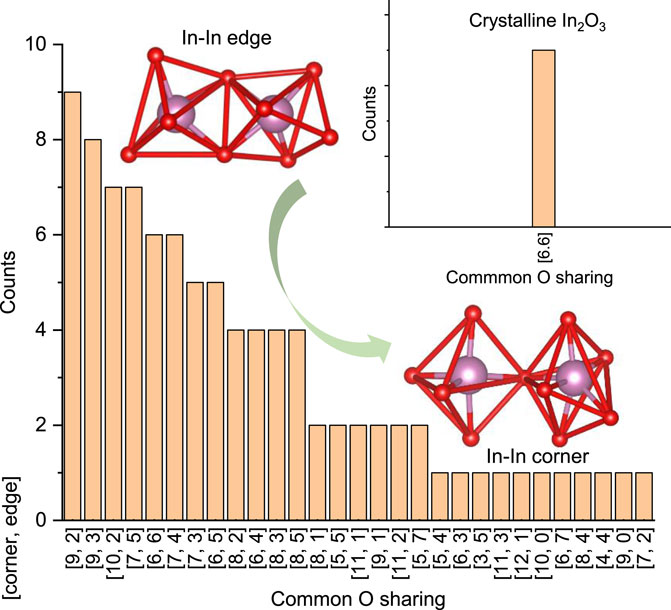
Figure 4. Statistics of In-In connectivity in a-In2O3. In the x-axis, [i, j] stands for coordination number of In-In through In-In common oxygen corner (i) sharing and edge sharing (j). i + j is the total CN of In-In. The inset shows the corresponding result in c-In2O3. Also shown as inserts are a typical In-In coordination through common oxygen edge sharing and a typical In-In coordination through common oxygen corner sharing. In c-In2O3, each In atom is coordinated to 6 In atoms through In-In edge connection (InO6 polyhedron sharing a common edge) and another 6 In atoms with In-In corner connection (InO6 polyhedron sharing a common corner). Upon amorphization, number of In-In corner sharing increases while number of In-In edge sharing decreases. Since In-In edge orbital overlap is more efficient than In-In corner, a-In2O3 has reduced electron conduction pathways comparing to c-In2O3.
The above results indicate that in a-In2O3 the local In-s/In-s orbital overlapping and In-In medium-range connection determine the electron transport effectiveness. The average In-In orbital overlapping integral quantifies the electron mobility in a-In2O3. It is well-known that in covalent bonded systems like Si and Ge, the amorphous phase mobilities typically degrade by 10–100 times compared to the crystalline phase mobility. (Clark, 1967; Marshall et al., 1986). In contrast, ionically bonded oxides can retain their high electron mobility in amorphous phases. (Nomura et al., 2004; Robertson, 2008). This is due to the spherical symmetry of s orbital which is immune from local structural distortion present in amorphous phase, while sp3-orbital overlaps are easily altered by local structure distortion. In our work, we found that the In-In coordination in a-In2O3, which is the structural origin for s-orbital overlap, does not disrupt significantly compared to c-In2O3. This is manifested by the slight change of In-In bond distance (3.39Å→3.44Å) and In CN of In (reducing from 12 in a-In2O3 to 11.5 in c-In2O3). The insignificant In-In connection change from crystalline to amorphous phase is the underlying reason for undisrupted s-orbital overlap in a-In2O3. The theoretical finding presented in this work can be validated by neutron diffraction experiment where the relationship between the In-In position correlation and electron mobility can be mapped. The above result implies that enhancing the In-In connection could improve the amorphous phase electron transport. For example, incorporating higher oxygen content during In2O3 thin film growth could tune In-In corner sharing into In-In edge sharing so that s-orbital overlap is strengthened. Densifying the film might decrease In-In bond distance and increase In-In CN, both of which are beneficial to In-In s-orbital overlap. These results could provide useful guidance for device engineers for better optimizing a-In2O3 based electronic devices.
4 Conclusion
In conclusion, we have investigated the electron conduction mechanism in In2O3 and its implication for amorphous phase transport from an orbital overlap facilitated electron transport perspective. Combined DFT and ETB calculations show that the electron transport is facilitated by the neighboring metal atomic s orbital overlap without oxygen’s p-orbital involvement. The ECP in In2O3 relies only on the metal-metal medium range connection. This electron conduction mechanism is extended to amorphous phase where the amorphous disorder influences the electron transport through impacting the metal-metal MRO including metal-metal CN and metal-metal separation. Our results contribute to the current theoretical understanding of electron transport in oxide semiconductors and to the practical advancement of oxides in technological applications.
Data availability statement
The original contributions presented in the study are included in the article/Supplementary Material, further inquiries can be directed to the corresponding author.
Author contributions
YH: Conceptualization, Data curation, Formal Analysis, Investigation, Methodology, Software, Validation, Visualization, Writing–original draft, Writing–review and editing. KC: Conceptualization, Funding acquisition, Methodology, Project administration, Resources, Software, Supervision, Writing–review and editing.
Funding
The author(s) declare that no financial support was received for the research, authorship, and/or publication of this article. This work was supported by ASCENT, one of the six centers in JUMP, a Semiconductor Research Corporation (SRC) program sponsored by Defense Advanced Research Projects Agency (DARPA).
Conflict of interest
The authors declare that the research was conducted in the absence of any commercial or financial relationships that could be construed as a potential conflict of interest.
Publisher’s note
All claims expressed in this article are solely those of the authors and do not necessarily represent those of their affiliated organizations, or those of the publisher, the editors and the reviewers. Any product that may be evaluated in this article, or claim that may be made by its manufacturer, is not guaranteed or endorsed by the publisher.
Supplementary material
The Supplementary Material for this article can be found online at: https://www.frontiersin.org/articles/10.3389/fmats.2024.1380180/full#supplementary-material
References
Blöchl, P. E. (1994). Projector augmented-wave method. Phys. Rev. B 50 (24), 17953–17979. doi:10.1103/physrevb.50.17953
Buchholz, D. B., Ma, Q., Alducin, D., Ponce, A., Jose-Yacaman, M., Khanal, R., et al. (2014). The structure and properties of amorphous indium oxide. Chem. Mat. 26 (18), 5401–5411. doi:10.1021/cm502689x
Chakraborty, W., Ye, H., Grisafe, B., Lightcap, I., and Datta, S. (2020). Low thermal budget (<250 °C) dual-gate amorphous indium tungsten oxide (IWO) thin-film transistor for monolithic 3-D integration. IEEE Trans. Electron Devices 67 (12), 5336–5342. doi:10.1109/ted.2020.3034063
Clark, A. H. (1967). Electrical and optical properties of amorphous germanium. Phys. Rev. 154 (3), 750–757. doi:10.1103/physrev.154.750
Fortunato, E., Barquinha, P., and Martins, R. (2012). Oxide semiconductor thin-film transistors: a review of recent advances. Adv. Mat. 24 (22), 2945–2986. doi:10.1002/adma.201103228
Harrison, W. A. (2012). Electronic structure and the properties of solids: the physics of the chemical bond. New York, NY: Courier Corporation.
Hu, Y., Hwang, J., Lee, Y., Conlin, P., Schlom, D. G., Datta, S., et al. (2019). First principles calculations of intrinsic mobilities in tin-based oxide semiconductors SnO, SnO2, and Ta2SnO6. J. Appl. Phys. 126 (18), 185701. doi:10.1063/1.5109265
Hu, Y., Schlom, D., Datta, S., and Cho, K. (2023a). Amorphous Ta2SnO6: a hole-dopable p-type oxide. Appl. Surf. Sci. 613, 155981. doi:10.1016/j.apsusc.2022.155981
Hu, Y., Schlom, D., Datta, S., and Cho, K. (2023b). Ilmenite and amorphous SnTiO3 as p-type oxide semiconductors. J. Mat. Chem. C 11 (14), 4830–4836. doi:10.1039/d2tc04937f
Hu, Y., Yao, X., Schlom, D. G., Datta, S., and Cho, K. (2020). First principles design of high hole mobility p-type Sn–O–X ternary oxides: valence orbital engineering of Sn2+ in Sn2+–O–X by selection of appropriate elements X. Chem. Mat. 33 (1), 212–225. doi:10.1021/acs.chemmater.0c03495
Ide, K., Nomura, K., Hosono, H., and Kamiya, T. (2019). Electronic defects in amorphous oxide semiconductors: a review. Phys. Status Solidi A 216 (5), 1800372. doi:10.1002/pssa.201800372
Kresse, G., and Furthmüller, J. (1996). Efficient iterative schemes for ab initio total-energy calculations using a plane-wave basis set. Phys. Rev. B 54 (16), 11169–11186. doi:10.1103/physrevb.54.11169
Kresse, G., and Hafner, J. (1994). Ab initio molecular-dynamics simulation of the liquid-metal–amorphous-semiconductor transition in germanium. Phys. Rev. B 49 (20), 14251–14269. doi:10.1103/physrevb.49.14251
Lee, S. Y. (2020). Comprehensive review on amorphous oxide semiconductor thin film transistor. Trans. Electr. Electron. Mat. 21 (3), 235–248. doi:10.1007/s42341-020-00197-w
Marshall, J., Street, R., and Thompson, M. (1986). Electron drift mobility in amorphous Si: H. Philos. Mag. B 54 (1), 51–60. doi:10.1080/13642818608243177
Nomura, K., Ohta, H., Takagi, A., Kamiya, T., Hirano, M., and Hosono, H. (2004). Room-temperature fabrication of transparent flexible thin-film transistors using amorphous oxide semiconductors. Nature 432 (7016), 488–492. doi:10.1038/nature03090
Nomura, K., Ohta, H., Ueda, K., Kamiya, T., Hirano, M., and Hosono, H. (2003). Thin-film transistor fabricated in single-crystalline transparent oxide semiconductor. Science 300 (5623), 1269–1272. doi:10.1126/science.1083212
Park, J. S., Maeng, W.-J., Kim, H.-S., and Park, J.-S. (2012). Review of recent developments in amorphous oxide semiconductor thin-film transistor devices. Thin Solid Films 520 (6), 1679–1693. doi:10.1016/j.tsf.2011.07.018
Pauling, L. (1929). The principles determining the structure of complex ionic crystals. J. Am. Chem. Soc. 51 (4), 1010–1026. doi:10.1021/ja01379a006
Perdew, J. P., Burke, K., and Ernzerhof, M. (1996). Generalized gradient approximation made simple. Phys. Rev. Lett. 77 (18), 3865–3868. doi:10.1103/physrevlett.77.3865
Perdew, J. P., Chevary, J. A., Vosko, S. H., Jackson, K. A., Pederson, M. R., Singh, D. J., et al. (1992). Atoms, molecules, solids, and surfaces: applications of the generalized gradient approximation for exchange and correlation. Phys. Rev. B 46 (11), 6671–6687. doi:10.1103/physrevb.46.6671
Robertson, J. (2008). Disorder and instability processes in amorphous conducting oxides. Phys. Status Solidi B 245 (6), 1026–1032. doi:10.1002/pssb.200743458
Salahuddin, S., Ni, K., and Datta, S. (2018). The era of hyper-scaling in electronics. Nat. Electron 1 (8), 442–450. doi:10.1038/s41928-018-0117-x
Shi, J., Zhang, J., Yang, L., Qu, M., Qi, D.-C., and Zhang, K. H. (2021). Wide bandgap oxide semiconductors: from materials physics to optoelectronic devices. Adv. Mat. 33 (50), 2006230. doi:10.1002/adma.202006230
Si, M., Hu, Y., Lin, Z., Sun, X., Charnas, A., Zheng, D., et al. (2020). Why In2O3 can make 0.7 nm atomic layer thin transistors. Nano Lett. 21 (1), 500–506. doi:10.1021/acs.nanolett.0c03967
Si, M., Murray, A., Lin, Z., Andler, J., Li, J., Noh, J., et al. (2021). BEOL compatible indium-tin-oxide transistors: switching of ultrahigh-density 2-D electron gas over 0.8×10¹⁴/cm2 at oxide/oxide interface by the change of ferroelectric polarization. IEEE Trans. Electron Devices 68 (7), 3195–3199. doi:10.1109/ted.2021.3061038
Takagi, A., Nomura, K., Ohta, H., Yanagi, H., Kamiya, T., Hirano, M., et al. (2005). Carrier transport and electronic structure in amorphous oxide semiconductor, a-InGaZnO4. Thin Solid Films 486 (1-2), 38–41. doi:10.1016/j.tsf.2004.11.223
Troughton, J., and Atkinson, D. (2019). Amorphous InGaZnO and metal oxide semiconductor devices: an overview and current status. J. Mat. Chem. C 7 (40), 12388–12414. doi:10.1039/c9tc03933c
Walsh, A., Da Silva, J. L., and Wei, S.-H. (2009). Interplay between order and disorder in the high performance of amorphous transparent conducting oxides. Chem. Mat. 21 (21), 5119–5124. doi:10.1021/cm9020113
Keywords: first principles, oxide semiconductor, mobility, tight binding, Amorphous phase
Citation: Hu Y and Cho K (2024) Electron conduction mechanism in indium oxide and its implications for amorphous transport. Front. Mater. 11:1380180. doi: 10.3389/fmats.2024.1380180
Received: 01 February 2024; Accepted: 07 March 2024;
Published: 25 March 2024.
Edited by:
Dongqi Zheng, Apple Inc., United StatesReviewed by:
Kedhareswara Sairam Pasupuleti, Chungnam National University, Republic of KoreaHanchul Kim, Sookmyung Women’s University, Republic of Korea
Copyright © 2024 Hu and Cho. This is an open-access article distributed under the terms of the Creative Commons Attribution License (CC BY). The use, distribution or reproduction in other forums is permitted, provided the original author(s) and the copyright owner(s) are credited and that the original publication in this journal is cited, in accordance with accepted academic practice. No use, distribution or reproduction is permitted which does not comply with these terms.
*Correspondence: Kyeongjae Cho, kjcho@utdallas.edu