Interfacial intermetallic compound modification to extend the electromigration lifetime of copper pillar joints
 Dongsheng Yang*
  Yilong Huang
- Guobo Electronics Co., Ltd., Nanjing, China
Electromigration is the massive metal atom transport due to electron flow, which could induce a disconnect in electronics. Due to the size of copper pillar bump reduction, the portion of interfacial intermetallic compound in solder joints is increasing obviously. However, there is lack of systematical research on the effects of intermetallic compound on the EM lifetime of solder joints. In this paper, the interfacial intermetallic compound of copper pillar joints is modified to extend the electromigration lifetime. The growth rate of intermetallic compound in solder joints sample is calculated firstly. From 230°C to 250°C, the growth rate of intermetallic compound increases from 0.09 μm/min to 0.19 μm/min. With a longer reaction time, the intermetallic compound layers continuously grow. Then electromigration tests were conducted under thermo-electric coupling loading of 100°C and 1.0 × 10⁴ A/cm2. Compared with lifetime of thin and thick intermetallic compound samples, the lifetime of all intermetallic compound sample improved significantly. The lifetime of thin, thick, and all intermetallic compound samples is 400 min, 300 min, and 1,200 min, respectively. The failure mechanism for the thin intermetallic compound sample is massive voids generation and aggregation at the interface between solder joints and pads. For the thick intermetallic compound sample, the intermetallic compound distance is short between cathode and anode in solder joints, leading to lots of crack create in the middle of solder joints. As the all intermetallic compound sample can greatly reduce the number of voids generated by crystal structure transforming, the lifetime extend obviously.
1 Introduction
To meet the requirement of the decrease of bump size and the increase of circuit density, the copper pillar bump for integrated circuit (IC) products has long been realized as one of the most promising solutions for high performance and high data rate electrical signal transmission (Hu et al., 2013). The first introduction of copper pillar bump is developed by IBM company in 1970, which is named as controlled collapse chip’s connect (C4) bumps (Naha et al., 2006). Usually, the copper pillar bumps compromise a Sn96.5Ag3.5 lead-free solder cap, used to bond metallization pads.
n electronics, solder joints in copper pillar bump sample will experience severe electromigration (EM) (Ma et al., 2016a; Ma et al., 2016b; Ding et al., 2022). Under the EM stress, crack can be observed in the copper pillar joints, and the cracks will accumulate, eventually leading to the failure of the entire electronic devices. In EM process, the atoms will massively transport along the direction of electron flow (Gu and Chan, 2008). Besides, Joule heating and current crowding are all associated with EM-induced failure of solder joints, which refers to the disconnection caused by the formation and growth of Kirkendall voids (Gu and Chan, 2008). Recently, many studies reported on EM in solder joints of copper pillar samples, and most of them focused on the mechanism of EM with various under bump metallurgies (UBMs) (Liang et al., 2006; Wang et al., 2012; Chen et al., 2015).
With the growing demand for smaller size and higher integration of microelectronics in electronic packaging, the size of solder joints in copper pillar bump has been gradually decreased (Ko et al., 2019). This means that higher current densities and temperature may occur in the solder joints, giving rise to EM. Thus, EM has become a more and more important indicator of joints reliability, which will determine the lifetime of the service time of electronic products (Song et al., 2020; Wang et al., 2020; Yue et al., 2021). In addition, copper pillar bump needs to be joined to pad by Sn96.5Ag3.5 solder in industry, and intermetallic compound (IMC) is formed through the interfacial reaction between solder and surface-finishing pad material during joining process (Mokhtar et al., 2021), (Xu et al., 2022). This IMC layer can affect the mechanical and electrical reliability of joints under the influence of EM. Due to size reduction, the proportion of IMC in solder joints of copper pillar is remarkably increased. In a particular case, there are even all IMC solder joints. Thus, it is essential to study the effects of IMC on the EM lifetime of solder joints.
The objective of this paper is to investigate the effects of IMC on the lifetime and the cracking failure of solder joints of copper pillar sample caused by EM under 100°C and 1.0 × 10⁴ A/cm2 thermo-electric coupling load. In addition, the growth rate of IMC in solder joints was evaluated.
2 Materials and methods
The copper pillar samples were provided by Advanced Semiconductor Limited, which were prepared by electroplating process and lithography process. As shown in Figure 1, Sn96.5Ag3.5 lead-free solder cap is electroplated on the copper pillar, and a (Cu,Ni)6Sn5 IMC layer formed between solder cap and copper pillar. The size of copper pillar is with diameter of 75 μm and height of 30 μm. To realize metallurgical connection, a pad is prepared, and metallization layers on pad are Cu/Ni/Au. The connection of copper pillar to pad was produced by hot pressing connection (HPC) process, which simultaneously applies pressure and heat. To observe the IMC growing process in solder joints, cross-sectional samples were prepared by mechanical polishing with SiC abrasive sandpaper (240#, 800#, 2000#, and 4,000#), and then polished with a 0.25 μm diamond suspension to eliminate surface scratches. The microstructure of solder joints was observed by a TESCAN Vega three scanning electron microscope (SEM) equipment at 10 kV.
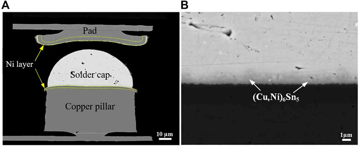
FIGURE 1. (A) The cross-sectional SEM image of copper pillar bump and pad (B) the IMC between solder cap and copper pillar.
3 Results
3.1 The growth rate of IMC layer
Usually, the IMC with thickness of 1–3 μm in solder joints is considered to process sufficient reaction between copper pillar bump and metallization pad. When thick IMC forms, voids and crack may occur in copper pillar joints, leading to shorter service time. Thus, it is necessary to study the growth rule of IMC in solder joints. The temperature and time are the two key parameters to control the IMC growth rate, with constant load of 1 MPa. The reaction temperature sets at 230°C, 240°C, and 250°C, respectively, and the reaction time is from 1 min to 10 min. The IMC thickness was calculated by the IMC area divided by the IMC length, while the IMC area and length were tested from SEM image.
Figure 2 indicates the relationship between heating parameters and IMC thickness of solder joints. Mathematical equations were used to fit the experimental data. At different heating temperature, the IMC is growing gradually with time increases, basically according to the equation of
where d is the thickness of IMC, t is the time, and D is the growth rate. By calculation, the growth rates of IMC are 0.09 μm/min at 230°C, 0.14 μm/min at 240°C, and 0.19 μm/min at 250°C. An obvious rule can be obtained that higher temperature can accelerate the growth rate of IMC. The reason is that higher temperature can increase the solution rate of Ni and Cu atoms to liquid solder, while the higher temperature beneficially accelerates the atomic reaction rate to form IMC. Longer time will extend the reaction to form more IMC at interface.
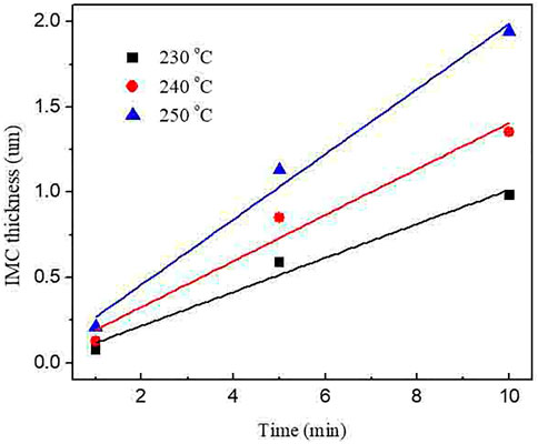
FIGURE 2. IMC thickness at interfa. ce heated at different temperature and time.
Figure 3 illustratesthe microstructure of IMC at different temperature and time. When sample sinter at 230°C for 1 min, very thin IMC formed and the elementary compositions are (Ni,Cu)3Sn4 and (Ni,Cu)3Sn. The result is similar to previous studies (Dai et al., 2022). When reaction time extends to 10 min, besides obvious thickness increase, the elementary composition transforms into (Cu,Ni)6Sn5. No more phase transformation is observed indicates that the (Cu,Ni)6Sn5 is stable crystal structure. When heating time increases to 240°C, the initial crystal structure of IMC is (Ni,Cu)Sn3, and it will also gradually transform into (Ni,Cu)6Sn5 at 10 min. By further increasing temperature to 250°C, the microstructure of IMC transforms quickly, and the initial (Ni,Cu)Sn3 will become to (Ni,Cu)6Sn5 at 5 min. Based on these research, it can be seen that the (Ni,Cu)3Sn4, (Ni,Cu)3Sn, and (Ni,Cu)Sn3 are transition crystal structures, and those structures will be eventually transformed into stable (Ni, Cu)6Sn5 structure. The reason for the crystal structure transformation principle is that, at the beginning of the soldering reaction, the liquid solder would provide sufficient Sn atoms. Thus, the Sn-rich crystal structures primarily grow. However, the formation energy of the alloy (Ni,Cu)6Sn5 is negative, so it is more thermodynamically stable and its alloying capacity is higher, resulting in automatic transformation from transition crystal structures to (Ni,Cu)6Sn5 structure (Leineweber et al., 2021). In summary, when there is sufficient atomic diffusion time, the final crystals structure is the (Ni,Cu)6Sn5 structure. Meanwhile, high temperature would accelerate the atomic diffusion rate, leading the faster crystal structure transformation from transition crystal structures to the most stable (Ni,Cu)6Sn5 structure.
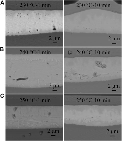
FIGURE 3. (A) IMC structure at 230°C at different time (B) IMC at 240°C, (C) IMC 250°C.
3.2 The daisy chain of copper pillar bumps
To study the effects of IMC on the electromigration lifetime of solder joints, a daisy chain of copper pillar bumps was designed. The daisy chain is composed of two substrates as shown in Figure 4. The copper pillar substrate contains two lead bonding pads, which are used to connect DC power. A 6 × 6 copper pillar array layouts on the substrate, and a metal wire prepared by electroplating connects each two copper pillars, with all copper pillars at non-conducting states. The other pad substrate has a 6 × 6 metallization pad array. Each two pads are connected by metal wire, with all pads at non-conducting states. The two paired substrates were bonding by hot pressing methods.
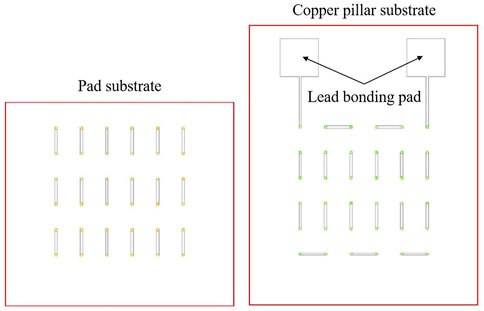
FIGURE 4. The schematic illustration of daisy chain.
3.3 Lifetime of solder joints
Based on the Arrhenius equation, improving temperature can significantly accelerate the atomic diffusion rate. Thus, to accelerate the atomic diffusion and shorten the research period, all experiments were conducted at environment of 100°C. The current density through solder joints sets at 1.0 × 10⁴ A/cm2. The experimental samples were placed on a hot plate, and the heating rate was 5°C/min. When the temperature reached at set value, the current stress was immediately loading to the samples. The failure criterion of solder joints is electrical open. Three kinds of solder joints were prepared to study the effects of IMC on lifetime of solder joints. Table 1 shows the IMC thickness and resistance of copper pillar daisy chain samples. The IMC thickness of thin, thick, and all IMC samples are 1.3 μm, 2.7 μm, and 10.1 μm, respectively. Figure 5 shows the initial microstructure of solder joints after reflow.
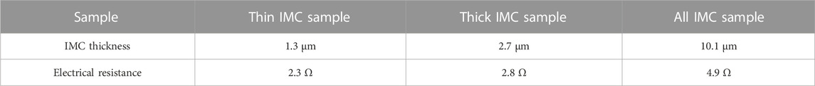
TABLE 1. The IMC thickness and electrical resistance of different samples.
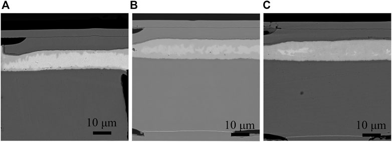
FIGURE 5. (A) Thin IMC sample (B) Thick IMC sample (C) All IMC sample.
Figure 6 shows the resistance change with time increase and cross-sectional image of failed solder joints. At simultaneous stresses of heat and electron flow, the resistance evolution of thin IMC sample could be divided into three steps. In the first step, the resistance has a huge increase from 2.3 Ω to 4.9 Ω. The obvious resistance change is due to quickly IMC increase. As we know, the conductivity of IMC crystal structure is obviously lower than that of Sn96.5Ag0.5 solder (The electrical resistivity of Cu6Sn5 and Sn is 17.5 mΩ cm and 10.9 mΩ cm, respectively) (Dai et al., 2022), (Zhu et al., 2020). Thicker IMC will continuously reduce the electric conduction of joints. In the second step, resistance of joint increases to 5.1 Ω and trend to be stable until to 250 min. After that, the resistance increases significantly until to 400 min when the daisy chain electrically failed. By observing the failed sample (Figure 6B), a crack close to the cathode side crosses the solder joint, but at the right corner of solder joints destruction is more serious. When the electron flow transports from cathode to anode, quick crystal structure transformation generates lots of voids in copper pillar and solder interface, which will finally aggregate to crack. Additionally, because the current tends to transmit along the least resistance pathway, there is a current crowding in the right corner. Therefore, the right corner near the cathode of solder joint has the highest failure risk.
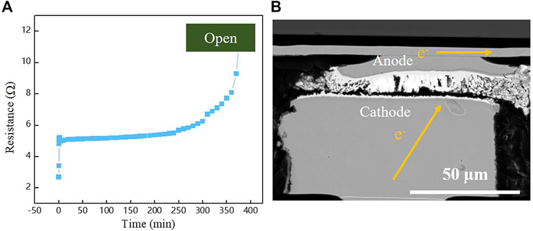
FIGURE 6. (A) The resistance evolution of thin IMC sample (B) the cross-sectional SEM image of failed thin IMC sample.
The same method is applied to monitor the resistance evolution of the thick IMC sample. Indicating in Figure 7A, there is a sharp increase in the initial few minutes, in which the resistance increases from 2.8 Ω to 5.1 Ω. In the second step after 10 min, the state of resistance is stable firstly and has a slight increasement after 150 min. Then, the growth rate of resistance gradually increases until to failure. Figure 7B shows microstructure of failure sample, lots of cracks form in the middle area of the joint. In this sample, initial IMC layer distance between copper pillar side and metallization pad side is less than 5 μm, voids generate at both anode and cathode will aggregate together. Thus, the time for crack crossing the solder joint unexpected shorten, resulting in a lifetime of thick IMC sample.
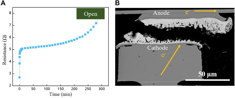
FIGURE 7. (A) The resistance evolution of thick IMC sample (B) the cross-sectional SEM image of failed thick IMC sample.
Unlike the thin and thick IMC samples, there is no quick resistance increase step being observed in all IMC joints, as shown in Figure 8A. Because all IMC crystal structure has formed completely. The lifetime of all IMC sample can reach about 1,200 min Due to the fact that there is no quick phase transformation during aging process, the failure of full IMC joint is due to high Joule heat caused by higher resistivity of IMC structure. In addition, the coefficient of thermal expansion (CTE) mismatch between pad materials and IMC cause mechanical stress in joints, which leads to crack initiation near cathode, as shown in Figure 8B. In the middle of joint, EM leads to several voids, but there are much less voids generating compared to thin and thick IMC joint. Under the electrical stress, the atoms of joints are moved by the electron wind force, leaving lots of voids in the joints, which is the main reason for EM failure. Because the interatomic force in IMC is much stronger than that in Sn96.5Ag3.5 solder, the atomic movement rate in all IMC joints is much slow than that in Sn96.5Ag3.5 solder. In summary, EM is not major factor of joint failure due to IMC excellent resistance to EM.
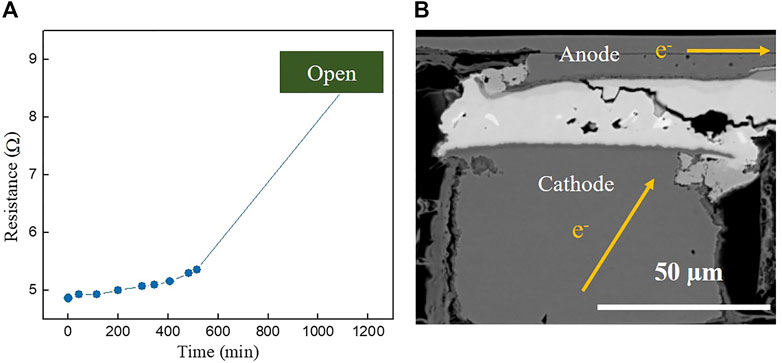
FIGURE 8. (A) The resistance evolution of all IMC sample, (B) the cross-sectional SEM image of failed all IMC sample.
By comparison, the solder joints with nearly 100% percent of IMC crystal structure have the highest lifetime, which is triple lifetime of thin IMC sample and four times of lifetime of thick IMC sample. The main reason is that all IMC sample can greatly reduce the number of voids, which are generated by crystal structure transforming. The research results in this study provide a novel solution to design long lifetime solder joints.
4 Conclusion
In this paper, the growth rate of IMC layer in solder joints of copper pillar samples was systematically investigated. The key parameters to control IMC growth rate are reaction temperature and time. Then, three IMC levels, 1.3 μm, 2.7 μm, and 10.1 μm, were selected to conduct electromigration tests on the copper pillar samples at ambient temperature of 100°C and current density of 1.0 × 10⁴ A/cm2. The effects of IMC on the lifetime of solder joints of copper pillar samples were tested. And also, microstructure evolution and failure modes of solder joints during electromigration have been investigated. The results of this study can be summarized as follows:
1) Higher temperature can accelerate the atomic reaction speed, and it also accelerates Ni and Cu atomic solution to liquid Sn96.5Ag3.5 solder, thus resulting in a quick IMC growth rate. Longer time can extend the atomic reaction time, which is beneficial the IMC growth. Meanwhile, it is found that the transition crystal structures would eventually transform into the most stable (Ni,Cu)6Sn5 structure.
2) For thin IMC sample, during the process of thermo-electric coupling loading, the IMC growth quickly in the initial few minutes, then stable for a longtime, and quickly failed at last. The lifetime of thin IMC sample is about 400 min. The failure mechanism is massive voids caused by EM generate and gather at the interface of solder joints.
3) Thick IMC sample has the shortest lifetime about 300 min, because IMC distance from cathode and anode is short, leading to lots of cracks occur in the middle of solder joints.
4) Due to the minimum crystal structure transformation and excellent EM resistance, all IMC sample has the longest lifetime, which is about 1,200 min. The reason for the excellent EM resistance of IMC is that the interatomic force in IMC is very strong. Thus, the atomic movement hardly occurs in IMC under current flow.
Data availability statement
The original contributions presented in the study are included in the article/supplementary material, further inquiries can be directed to the corresponding author.
Author contributions
Conceptualization, DY; methodology, DY; software, YH; validation YH; investigation, DY; data curation, YH; writing—original draft preparation, DY; writing—review and editing, YH; supervision, DY; project administration, DY. All authors have read and agreed to the published version of the manuscript.
Conflict of interest
Authors DY and YH were employed by the company Guobo Electronics Co., Ltd.
Publisher’s note
All claims expressed in this article are solely those of the authors and do not necessarily represent those of their affiliated organizations, or those of the publisher, the editors and the reviewers. Any product that may be evaluated in this article, or claim that may be made by its manufacturer, is not guaranteed or endorsed by the publisher.
References
Chen, H., Hang, C., Fu, X., and Li, M. (2015). Microstructure and grain orientation evolution in Sn-3.0Ag-0.5Cu solder interconnects under electrical current stressing. J. Electron. Mat. 44, 3880–3887. doi:10.1007/s11664-015-3922-2
Dai, J., Zhang, Y., Li, Z., Chen, M., Guo, Y., Fan, Z., et al. (2022). Research on reliability of Ni/Sn/Cu(Ni) copper pillar bump under thermoelectric loading. J. Electron Packag. 144, 031014. doi:10.1115/1.4053889
Ding, Z. F., Wang, X-J., Wang, W. D., Cai, S. S., Guo, J. D., and Zhu, Q. S. (2022). Severe embrittlement of copper pillar bumps electrodeposited using JGB as leveler. J. Mat. Sci. Mat. Electron 33, 19026–19035. doi:10.1007/s10854-022-08741-5
Gu, X., and Chan, Y. C. (2008). Electromigration in line-type Cu/Sn-Bi/Cu solder joints. J. Electron. Mat. 37, 1721–1726. doi:10.1007/s11664-008-0539-8
Hu, Y. C. X., Chan, K., Zhang, K. C., and Yung, E. (2013). Effect of graphene doping on microstructural and mechanical properties of Sn–8Zn–3Bi solder joints together with electromigration analysis. J. Alloys Compd. 580, 162–171. doi:10.1016/j.jallcom.2013.05.124
Ko, Y.-H., Kirak, S., Kim, G., Park, Y. B., Yu, D.-Y., Bang, J., et al. (2019). Effects of graphene oxide on the electromigration lifetime of lead-free solder joints. J. Mat. Sci.-Matter. El. 0, 2334–2341. doi:10.1007/s10854-018-0506-y
Leineweber, A., Löffler, M., and Martin, S. (2021). Stable and metastable phase equilibria involving the Cu6Sn5 Intermetallic. J. Electron. Mat. 50, 5898–5914. doi:10.1007/s11664-021-09067-4
Liang, S. W., Chang, Y. W., and Chen, C. (2006). Effect of Al-trace dimension on Joule heating and current crowding in flip-chip solder joints under accelerated electromigration. Appl. Phys. Lett. 88, 172108. doi:10.1063/1.2198809
Ma, H.-C., Guo, J.-D., Chen, J.-Q., Wu, D., Liu, Z.-Q., Zhu, Q.-S., et al. (2016). The reliability of copper pillar under the coupling of thermal cycling and electric current stressing. J. Mat. Sci. Mat. Electron 27, 9748–9754. doi:10.1007/s10854-016-5038-8
Ma, H., Guo, J., Chen, J., Wu, D., Liu, Z., Zhu, Q., et al. (2016). Prediction model of lifetime for copper pillar bumps under coupling effects of current and thermal cycling. J. Mat. Sci. Mat. Electron 27, 1184–1190. doi:10.1007/s10854-015-3871-9
Mokhtar, N. Z. M., Salleh, M. A. A. M., Sandu, A. V., Ramli, M. M., Chaiprapa, J., Vizureanu, P., et al. (2021). Effect of electromigration and thermal ageing on the tin Whiskers’ formation in thin Sn-0.7Cu-0.05Ga lead (Pb)-free solder joints. Coatings 11, 935. doi:10.3390/coatings11080935
Naha, J. W., Suh, J. O., Tu, K. N., Yoon, S. W., Rao, V. S., Kripesh, V., et al. (2006). Electromigration in flip chip solder joints having a thick Cu column bump and a shallow solder interconnect. J. Appl. Phys. 100, 123513. doi:10.1063/1.2402475
Song, J.-M., Huang, B.-C., Tarng, D., Hung, C.-P., and Yasuda, K. (2020). Relationship between nanomechanical responses of interfacial intermetallic compound layers and impact reliability of solder joints. Nanomaterials 10, 1456. doi:10.3390/nano10081456
Wang, Y., Lu, K. H., Gupta, V., Stiborek, L., Shirley, D., Chae, S. H., et al. (2012). Effects of Sn grain structure on the electromigration of Sn-Ag solder joints. J. Mat. Res. 27, 1131–1141. doi:10.1557/jmr.2012.10
Wang, Z.-Y., Dang, N. M., Wang, P.-H., Chen, T. Y.-F., and Lin, M.-T. (2020). Study on electromigration effects and IMC formation on Cu–Sn films due to current stress and temperature. Appl. Sci. 10, 8893. doi:10.3390/app10248893
Xu, K., Fu, X., Wang, X., Fu, Z., Yang, X., Chen, S., et al. (2022). The Effect of grain orientation of β-Sn on copper pillar solder joints during electromigration. Materials 15, 108. doi:10.3390/ma15010108
Yue, W., Ding, C., Qin, H., Gong, C., and Zhang, J. (2021). Crystallographic characteristic effect of Cu substrate on serrated cathode dissolution in Cu/Sn–3.0Ag–0.5Cu/Cu solder joints during electromigration. Materials 14, 2486. doi:10.3390/ma14102486
Keywords: solder joint, electromigration, copper pillar bump, interfacial intermetallic compound, electromigration (EM)
Citation: Yang D and Huang Y (2023) Interfacial intermetallic compound modification to extend the electromigration lifetime of copper pillar joints. Front. Mater. 9:1080848. doi: 10.3389/fmats.2022.1080848
Received: 26 October 2022; Accepted: 10 November 2022;
Published: 04 January 2023.
Edited by:
Xiangchen Meng, Harbin Institute of Technology, ChinaCopyright © 2023 Yang and Huang. This is an open-access article distributed under the terms of the Creative Commons Attribution License (CC BY). The use, distribution or reproduction in other forums is permitted, provided the original author(s) and the copyright owner(s) are credited and that the original publication in this journal is cited, in accordance with accepted academic practice. No use, distribution or reproduction is permitted which does not comply with these terms.
*Correspondence: Dongsheng Yang, yangds2021@hotmail.com