Sulfurization of Electrodeposited Sb/Cu Precursors for CuSbS2: Potential Absorber Materials for Thin-Film Solar Cells
 Aimei Zhao1 Yanping Wang1 Bing Li1
  Dongmei Xiang1 Zhuo Peng1 Yujie Yuan1 Yupeng Xing1 Liyong Yao2
  Jinlian Bi1* Wei Li1*
- 1Tianjin Key Laboratory of Film Electronic and Communication Devices, School of Integrated Circuit Science and Engineering, Tianjin University of Technology, Tianjin, China
- 2Tianjin Institute of Power Source, Tianjin, China
CuSbS2, as a direct bandgap semiconductor, is a promising candidate for fabricating flexible thin-film solar cells due to its low grain growth temperature (300°C–450°C). Uniform and highly crystalline CuSbS2 thin films are crucial to improving device performance. However, uniform CuSbS2 is difficult to obtain during electrodeposition and post-sulfurization due to the “dendritic” deposition of Cu on Mo substrates. In this study, Sb/Cu layers were sequentially pulse electrodeposited on Mo substrates. By adjusting the pulse parameters, smooth and uniform Sb layers were prepared on Mo, and a flat Cu layer was obtained on Sb without any dendritic clusters. A two-step annealing process was employed to fabricate CuSbS2 thin films. The effects of temperature on phases and morphologies were investigated. CuSbS2 thin films with good crystallinity were obtained at 360°C. As the annealing temperature increased, the crystallinity of the films decreased. The CuSbS2 phase transformed into a Cu3SbS4 phase with the temperature increase to 400°C. Finally, a 0.90% efficient solar cell was obtained using the CuSbS2 thin films annealed at 360°C.
Introduction
CuSbS2 is a direct bandgap material, which can be adjusted between 1.4 and 1.6 eV (Medina-Montes et al., 2018; Pal et al., 2020), and its optical absorption coefficient is greater than 105 cm−1 (Vinayakumar et al., 2019). Its grain growth temperature is within 300°C–450°C (Yang et al., 2014; Riha et al., 2017), which is lower than those of Cu (In, Ga) Se2 and Cu2ZnSnS4. It is an excellent alternative material for flexible photovoltaic devices due to its low grain growth temperature. Various techniques, such as spray pyrolysis (Ramos Aquino et al., 2016; Wan et al., 2019; Zhou et al., 2021), ink (Banu et al., 2016; Banu et al., 2019), chemical bath deposition (Macías et al., 2017; Loranca-Ramos et al., 2018), sputtering (de Souza Lucas et al., 2016; Kang et al., 2018), evaporation (Rabhi et al., 2009; Wan et al., 2016), and electrodeposition (Septina et al., 2014; García et al., 2020), have been employed to fabricate CuSbS2 thin films. Wan et al., (2016) fabricated stoichiometric CuSbS2 thin films and Mo/CuSbS2/CdS/ZnO/ZnO: Al/Ag structure solar cells via a two-stage co-evaporation, achieving a 1.9% efficiency with a 520-mV open-circuit voltage. Macías et al., (2017) fabricated CuSbS2 thin films via a chemical bath method and treated the films at 380°C, achieving an encouraging efficiency of 0.6%. Zhang et al.(2019) fabricated Mo/CuSbS2/CdS/ZnO/Al structure cells via a one-step sputtering method and obtained a photovoltaic conversion efficiency of 2.55% with a 622-mV open-circuit voltage. The best efficiency of 3.22% was obtained by Banu et al., (2016).
Compared with other deposition methods, electrodeposition has the advantages of low equipment cost, simple operation, and high material usage rate (Lincot et al., 2004; Bhattacharya et al., 2012; Oliva et al., 2013; Vauche et al., 2016). Therefore, fabricating CuSbS2 thin films via electrodeposition has been favored by researchers. The highest efficiency of CuSbS2 thin films fabricated via electrodeposition is 3.13% (Septina et al., 2014), which is far lower than the maximum theoretical conversion efficiency of 22.9% (SLME) (Yu et al., 2013). The main factor limiting the further improvement of CuSbS2 thin-film solar cells are 1) rough electrodeposited metal precursors lead the thickness and composition distribution to be nonuniform (Yuan et al., 2009; Gao et al., 2020)and 2) secondary phases, such as Sb2S3, Cu12Sb4S13, and Cu3SbS4, easily form during annealing (Kang et al., 2018; Pal et al., 2020).
Zhang et al. (2016) have demonstrated the crystallinity of CuSbS2 thin films fabricated by electrodepositing Mo/Cu/Sb metal layers followed by sulfurizing in 20% H2S + Ar atmosphere for 1 h at 450°C. However, the surface roughness of the Mo/Cu/Sb metal layers was large, which further deteriorated the uniformity of CuSbS2 thin films. Although Bi et al. (2016) eliminated the dendritic morphology of Cu on Mo via a pulse current electrodeposition method, the problem of dendritic clusters appeared again after the Cu thickness was reduced. To fabricate dendritic-cluster-free and smooth Cu films via electrodeposition, numerous studies have been conducted (Norkus et al., 2005; Moffat et al., 2007; Lee et al., 2012). Among them, adding organic additives in the electrodepositing solution could help reduce the surface roughness of Cu films and improve their flatness (Long et al., 2006; Favry et al., 2008). However, organic additives could easily be incorporated into the films as impurities, which would deteriorate the properties of the devices.
In this study, to solve the problem of rough metal precursors on Mo substrates, first, a smooth Sb layer was electrodeposited on a Mo substrate, and then, a Cu layer was electrodeposited on the Sb layer. A compact, flat, and uniform Sb/Cu layer was fabricated on a Mo substrate using the pulse current electrodeposition method. The metal stacking layer with the Sb/Cu atomic ratio of 1.7 was employed to fabricate CuSbS2. In addition, the influences of temperature on structures, compositions, phases, and morphologies of CuSbS2 thin films were systematically studied. Ultimately, 0.90% efficient CuSbS2 solar cells were fabricated with a 13.58-mA/cm2 current density.
Materials and Methods
Preparation of the Sb/Cu Precursor
Mo back contact layer (1 μm) was fabricated on a clean soda-lime glass (SLG) via DC magnetron sputtering. Before the electrodeposition process, the fabricated SLG/Mo substrate was ultrasonically cleaned in alcohol for 30 min, followed by cleaning with deionized water to obtain a clean, oil-free Mo substrate. Afterward, Sb and Cu metal layers were fabricated on the Mo substrate via pulse electrodeposition at room temperature. An Sb solution was prepared using 0.3-M SbCl3 and 2.2-M HCl, whereas a Cu solution was prepared using 0.8-M CuSO4 and 0.76-M H2SO4. The diagram of the square wave pulse is shown in Supplementary Figure S1. There are three independent parameters: pulse current density (im), pulse on time (Ton), and pulse off time (Toff) in pulse electrodeposition. Toff is beneficial to recover ion concentration near a cathode and improve the coating quality. The Ton/Toff ratios of the electrodeposited Sb film were set to 1:1, 1:3, and 1:5; the pulse current densities were 31.25, 62.5, and 125 mA/cm2; and the pulse frequency was 10,000 Hz. The Ton/Toff ratio of the electrodeposited Cu film was 1:3, the pulse current density was 62.5 mA/cm2, and the pulse frequency was 10,000 Hz. The deposition charge densities of the Sb layer were varied from 0.5 to 1.275 C/cm2. The pulse working conditions were provided by GKPT-FB4-24 V/10 A pulse/DC power supply manufactured by Shenzhen Shicheng Company, China.
Sulfurization of the Metal Precursor
CuSbS2 thin films were fabricated by annealing Mo/Sb/Cu precursors in a double temperature quartz tube furnace. The alloyed precursor and 1-g sulfur powder (excess) were, respectively, placed in different temperature zones of the double temperature quartz tube furnace. The sulfur source temperature was maintained at 260°C with a 10°C/min heating rate. First, the metal stacks were annealed at 320°C in Ar atmosphere for 10 min and then sulfurized at 300°C–400°C for another 30 min. After free cooling to room temperature, the CuSbS2 thin films were removed from the furnace.
Preparation of Devices
CuSbS2 thin-film solar cells were prepared with the traditional structure of Mo/CuSbS2/CdS/i-ZnO/ZnO: Al/Ni/Al. A CdS buffer layer of 50 nm was prepared via the chemical water bath method on CuSbS2 thin films. The i-ZnO thin films with approximately 50-μm thickness were deposited on CdS thin films by AC magnetron sputtering; then, the Al-ZnO thin films with 500–800 nm thickness were deposited by DC sputtering. Finally, a Ni layer of 50 nm and an Al layer of 1 μm were deposited by electron beam evaporation as the collector. The effective area of the cell was 0.12 cm2.
Characterization
The structure of the CuSbS2 thin films was analyzed using X-ray diffractometry (XRD, Rigaku Smart Lab) and Raman spectrometry (Raman, Renishaw). The excitation wavelength of the Raman spectrometer was 532 nm. The surface roughness of the films was observed via atomic force microscopy (AFM, Dimension ICON). The morphology of the films and the elemental composition and distribution (EDS) of the samples were observed via field emission scanning electron microscopy (FE-SEM, Quanta FEG 250). The element composition and chemical states of the films were measured via energy-dispersive X-ray spectrometry (XPS, ESCALAB250Xi). The J−V characteristics of CuSbS2 solar cells were measured under a standard AM_1.5 spectrum using a solar simulator; the illumination intensity was 1000 WM−2.
Results and Discussion
Characteristics of the Sb/Cu Metal Precursors
Figure 1 shows the SEM images of Cu and Cu/Sb deposited on the Mo substrate. From Figure 1A, a “dendritic” morphology was formed by directly depositing the Cu layer on the Mo substrate. It was because the growth of Cu on Mo showed a three-dimensional island mode (Mercier et al., 2013). The growth rate of the Cu nucleus tended to be higher than the nucleation rate, inducing Cu to form a dendritic morphology (Budevski et al., 2000). The Sb layer electrodeposited on such a rough Cu underlayer usually resulted in a coarse Cu/Sb layer with bulging clusters on the Sb surface (Figure 1B). The non-uniform composition distribution of the rough Cu/Sb precursor tended to form copper-rich and -poor phases during annealing, which would increase the leakage current of the device and deteriorate its performance (Oliva et al., 2013; Kwon et al., 2014).
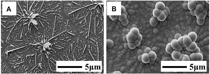
FIGURE 1. SEM images of the (A) Mo/Cu and (B) Mo/Cu/Sb layers.
To eliminate the “dendritic” morphology, the Mo/Sb/Cu stack was employed to obtain a flat and uniform metal precursor. Figure 2 shows the SEM images of the Sb layer on Mo prepared via the pulse current electrodeposition method. In Figures 2A–C, the Ton/Toff ratio was set to 1:1, 1:3, and 1:5, with the pulse current density of 62.5 mA/cm2; small spherical grains can be observed. The size of the spherical grains was relatively non-uniform with the Ton/Toff ratio of 1:1. The spherical grain size tended to be uniform with the decrease in the Ton/Toff ratio, and the surface of Sb films became smooth and compact. When the ratio decreased to 1:5, the Sb grains became nonuniform again. It might be because the decreased Ton/Toff ratio increased the peak current density, which led the growth rate of the Sb nucleus to be higher than the nucleation rate (Grujicic and Pesic, 2002).
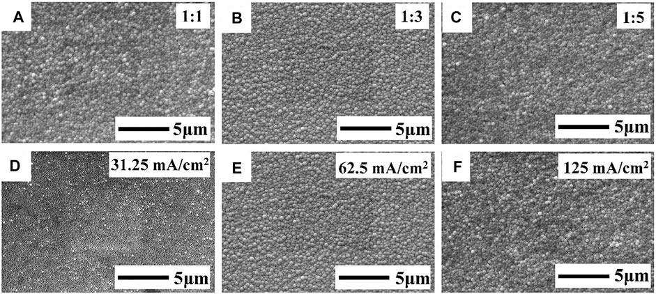
FIGURE 2. FE-SEM images of the Sb film on the Mo substrate deposited with (A–C) Ton/Toff ratios of 1:1, 1:3, and 1:5, respectively, and a pulse current density of 62.5 mA/cm2; (D–F) pulse current densities of 31.25, 62.5, and 125 mA/cm2 and a Ton/Toff ratio of 1:3.
Figures 2D–F show the FE-SEM images of Sb deposited with different pulse current densities: 31.25, 62.5, and 125 mA/cm2. The Ton/Toff ratio was set to 1:3. The Sb surface was covered with a layer of insect-like particles with a pulse current density of 31.25 mA/cm2. It might be because the Sb film was not fully nucleated and grew up when the current density was too low. When the pulse current density increased to 62.5 mA/cm2, a uniform and compact Sb film was obtained. However, an uneven surface appeared when the pulse current density increased to 125 mA/cm2, which might be due to the concentration polarization near the surface of Sb film at high pulse current density. Finally, a uniform, flat, and compact Sb film could be fabricated on the Mo substrate with a Ton/Toff ratio of 1:3 and a pulse current density of 62.5 mA/cm2.
The Sb film deposited with a pulse current density of 62.5 mA/cm2 and Ton/Toff of 1:3 (Figure 2B) was chosen as the substrate to deposit the Cu layer. The Cu was deposited with a pulse current density of 62.5 mA/cm2 and a pulse frequency of 10,000 Hz. Figure 3 shows a smooth, compact Cu layer without any dendritic clusters being obtained.
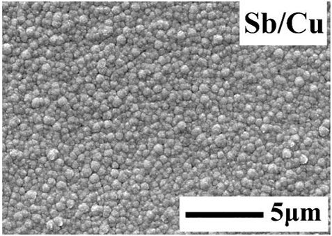
FIGURE 3. SEM image of the Mo/Sb/Cu layer.
Figure 4 presents the AFM images of Mo/Cu, Mo/Cu/Sb, Mo/Sb, and Mo/Sb/Cu layers. The average roughness (Ra) of each layer was calculated using an atomic force microscope assistant software (Table 1). The average roughness (Ra) of Mo/Cu (96 nm) was larger than that of Mo/Sb (21.8 nm). As the underlying layer, the surface roughness of the Mo/Cu/Sb layer (112 nm) was larger than that of the Mo/Sb/Cu layer (30.4 nm), indicating that the uniformity of Mo/Sb/Cu was higher than that of Mo/Cu/Sb. Therefore, the new structure of Mo/Sb/Cu was chosen as the metal precursor to fabricate CuSbS2 absorbers.
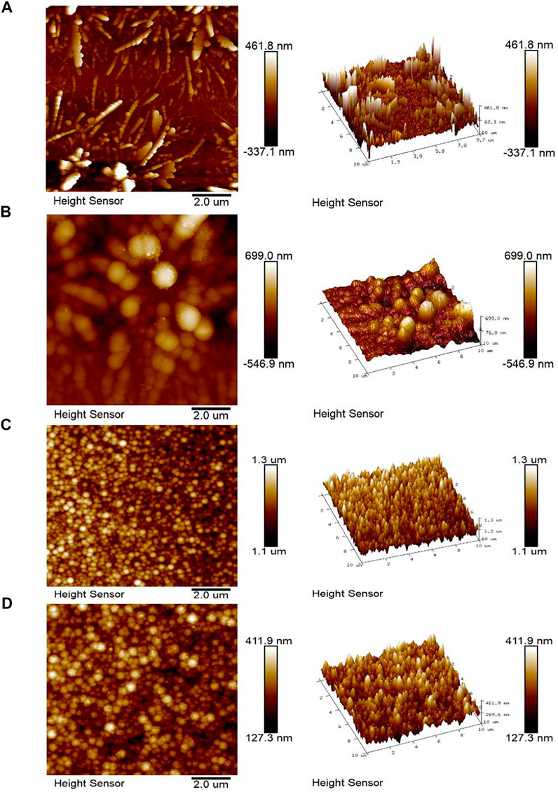
FIGURE 4. AFM diagrams of the (A) Mo/Cu, (B) Mo/Cu/Sb, (C) Mo/Sb, and (D) Mo/Sb/Cu layers.
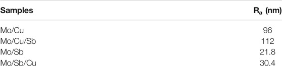
TABLE 1. Surface roughness of the Mo/Cu, Mo/Cu/Sb, Mo/Sb, and Mo/Sb/Cu layers.
Analysis of the Composition, Phase, and Morphology of the CuSbS2 Thin Film
Sb2S3 is easy to evaporate in the sulfurization process due to its high saturated vapor pressure, resulting in the loss of Sb elements. Therefore, the Sb/Cu metal-stack layers with an atomic ratio of 1.7 were sulfurized to prepare CuSbS2 absorbers. Figure 5A shows the XRD patterns of the CuSbS2 thin films annealed at 300, 320, 340, 360, 380, and 400°C for 30 min. The sample sulfurized at 300°C detected the CuSbS2 chalcostibite compound (JCPDS No. 44-1417) and weak diffraction peaks of Sb2S3 (JCPDS No. 42-1393) and Cu2−xS. The CuSbS2 phase was generated by the reaction of Cu and Sb chalcogenides. Cu was completely transformed into Cu-S at 200°C, whereas Sb reacted with S to form Sb2S3 at approximately 300°C. When the temperature was sufficiently high (300°C), the binary sulfides of Cu and Sb reacted to form the CuSbS2 ternary compound. The specific reaction equations are as follows (Colombara et al., 2012):
With the increase in temperature, the intensity of the Sb2S3 secondary phase decreased and the crystallinity of CuSbS2 thin films improved. In the temperature range of 320°C–340°C, the films mainly comprised CuSbS2 and Sb2S3 phases. However, the diffraction peak intensity of CuSbS2 gradually increased with the temperature increase, whereas the intensity of the Sb2S3 peak gradually decreased. At 360°C, the typical bimodal structure of the CuSbS2 phase was observed in the range of 28°–31°. In addition, the CuSbS2 thin film showed the (301) preferred orientation. No other obvious secondary phases were observed, indicating that the film was relatively pure. Sb2S3 might have evaporated during high-temperature sulfurization due to its relatively high saturated vapor pressure (Colombara et al., 2011; Colombara et al., 2012). When the temperature increased to 380°C, the diffraction peak of CuSbS2 began to decrease; the preferential orientation of the CuSbS2 thin films changed from (301) to (410). When the annealing temperature increased to 400°C, the films became Cu-rich due to the loss of a large amount of Sb, and the CuSbS2 phase transformed into the Cu3SbS4 phase (JCPDS No. 35-0581). CuSbS2 tended to decompose into Cu3SbS4 and Sb2S3. The diffraction peak of Sb2S3 was not detected, because Sb2S3 evaporated due to its low melting point. The decomposition reaction was as follows:
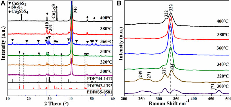
FIGURE 5. (A) XRD patterns and (B) Raman spectra of CuSbS2 thin films sulfurized at different substrate temperatures: 300°, 320°, 340°, 360°, 380°, and 400°C.
Figure 5B presents the Raman spectra of films annealed at different sulfurization temperatures. Raman vibration peaks at 249, 317, and 339–332 cm−1 all corresponded to the CuSbS2 phase, as reported previously (Vinayakumar et al., 2017; Chalapathi et al., 2018). Moreover, the Raman peak at 471 cm−1 of the film sulfurized at 300°C corresponded to the Cu2−xS phase (Hurma and Kose, 2016), which agreed with the XRD results. Besides, the Raman peak at 271 cm−1 of the films sulfurized in the temperature range of 300°C–340°C corresponded to the Sb2S3 secondary phase (Efthimiopoulos et al., 2016). No Cu2−xS phase was detected in the films annealed in the temperature range of 320°C–340°C, indicating that Cu2−xS and Sb2S3 had reacted completely to form CuSbS2. At 360°C, there was a prominent peak at 332 cm−1, which corresponded to CuSbS2. With the increase in the crystallization degree, the secondary peaks at 317 cm−1 disappeared and only the main peak located at 332 cm−1 remained. At 400°C, a shoulder at 322 cm−1 appeared due to the existence of the Cu3SbS4 phase (Chalapathi et al., 2018).
The elemental compositions of the films at different annealing temperatures were determined via EDS (Table 2). The compositions of Cu, Sb, and S were very sensitive to the annealing temperature. The films were rich in copper and poor in antimony due to the high volatility of Sb2S3. The Cu/Sb ratio was approximately 2.5 in the temperature range of 300°C–340°C, and the ratio decreased with the increase in temperature. This is because Sb was not fully sulfurized into Sb2S3 and did not fully participate in the reaction to generate CuSbS2. When the temperature increased to 360°C, CuS and Sb2S3 fully reacted to produce CuSbS2, the film showed only a slight Cu-rich composition and the Cu/Sb ratio of the film decreased to 1.06. Sb loss was significant when the temperature further increased to 400°C. The Cu/Sb ratio increased to 2.81 at 400°C, which should be due to the decomposition of the membrane into Cu3SbS4.
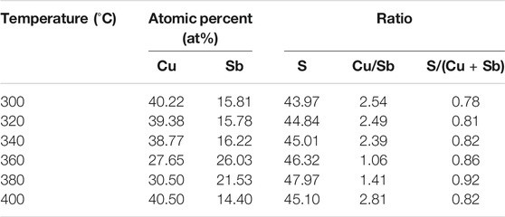
TABLE 2. Elemental compositions of thin films annealed at different temperatures measured via EDS.
Figure 6 shows the FE-SEM images of the films sulfurized at different temperatures. The morphologies of the CuSbS2 thin films changed with the increase in temperature. As shown in Figure 6A, fine grains and white rod-shaped grains were observed on the film surface. EDS analysis showed that the white rod-shaped grains were Cu- and S-rich phases. In the temperature range of 320°C–340°C, grains began to aggregate and grow up. With the increase in temperature, the grain sizes increased. In the temperature range of 360°C–380°C, micron-sized rod-like grains were formed and the crystallization degree and compactness of CuSbS2 thin films improved. Notably, the surface morphology of the film changed significantly with the increase in temperature due to the low reaction and formation temperature of CuSbS2. However, further increasing the growth temperature to 400°C, the pores formed on the film surfaces. Combined with the XRD and Raman analyses, this phenomenon might be due to the decomposition of the CuSbS2 phase—where a large amount of Sb loss destroyed the completeness of the film. A relatively pure CuSbS2 thin film could be obtained in the temperature range of 360°C–380°C.
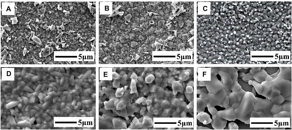
FIGURE 6. FE-SEM images of the CuSbS2 thin films annealed at different temperatures: (A) 300°C, (B) 320°C, (C) 340°C, (D) 360°C, (E) 380°C, (F) 400°C.
Figure 7 shows the cross-sectional FE-SEM images of the films sulfurized at 360 and 380°C. The thickness of the films was approximately 1.2 μm without fine-grain layers at the bottom of the film. At 360°C, the adhesion between the annealed Mo and CuSbS2 thin films was good and columnar large grains were formed. The CuSbS2 grain sizes increased with the increase in the sulfurization temperature to 380°C. Compared with the films prepared at 380°C, the films prepared at 360°C were more uniform and denser. The crystallinity of the CuSbS2 thin films annealed at 360°C was high and more suitable to prepare CuSbS2 devices.
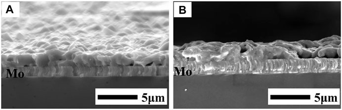
FIGURE 7. Cross-sectional SEM images of CuSbS2 thin films annealed at (A) 360°C and (B) 380°C.
XPS Analysis of the CuSbS2 Thin Films
XPS was employed to measure the chemical states of elements in the CuSbS2 thin films sulfurized at 360°C (Figure 8). From Figure 8A, the main elements of CuSbS2 thin films were Cu, Sb, and S, indicating no additional doping element in the CuSbS2 thin film. As shown in Figures 8B–D, the binding energies of Cu 2p1/2 and 2P3/2 were 931.9 and 951.7 eV, respectively, with an interval of 19.8 eV, which agreed with the reported binding energies of Cu+ in CuSbS2 (Wan et al., 2016). The binding energies of Sb 3d5/2 and 3d3/2 were 529.6 and 539.0 eV, respectively, with an interval of 9.4 eV, which agreed with Sb3+ (Vinayakumar et al., 2017). The peak at 532.1 eV corresponded to the oxygen adsorbed on the thin film. The binding energies of S 2p3/2 and 2p1/2 were 161.4 and 162.6 eV, respectively, with an interval of 1.2 eV, which corresponded to the binding energies of S2− in CuSbS2 (van Embden et al., 2020). The results agreed with the chemical states of standard CuSbS2, which proved the pure phase CuSbS2 thin films to be prepared at the annealing temperature of 360°C.
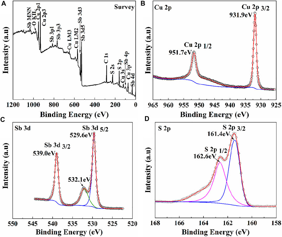
FIGURE 8. XPS of the CuSbS2 thin films prepared at 360°C. (A) Survey, (B) Cu 2p core level, (C) Sb 3 days core level, and (D) S 2p core level.
The CuSbS2 thin films annealed at 360°C and 380°C were selected to prepare solar cells. The J–V curves of the CuSbS2 thin-film solar cells are shown in Figure 9. The device parameters are listed in Table 3. The photovoltaic conversion efficiency (η) of the device, based on the CuSbS2 thin films annealed at 360°C, was 0.90% with an open-circuit voltage (Voc) of 0.21 V, a current density (Jsc) of 13.58 mA/cm2, and a filling factor (FF) of 31.77%. However, the photovoltaic conversion efficiency of the device, based on the CuSbS2 film annealed at 380°C, was only 0.36% with an open-circuit voltage(Voc) of 0.10 V, a current density of 11.75 mA/cm2. The CuSbS2 thin films annealed at 360°C were more compact than those annealed at 380°C (Figures 6D,E). The voids in the CuSbS2 thin films could influence carrier transportation, which would reduce the current density. Combined with the XRD analysis, the crystal-preferred orientation of the CuSbS2 thin films changed from (301) to (410) with an increase in annealing temperature. Based on the analysis of the Cu (In, Ga) Se2-preferred orientation (Kim et al., 2018), the changed-preferred orientation of CuSbS2 might induce different defect densities, which would influence the open-circuit voltage. In addition, the band structure diagram of CuSbS2 thin film solar cells is shown in Supplementary Figure S2.
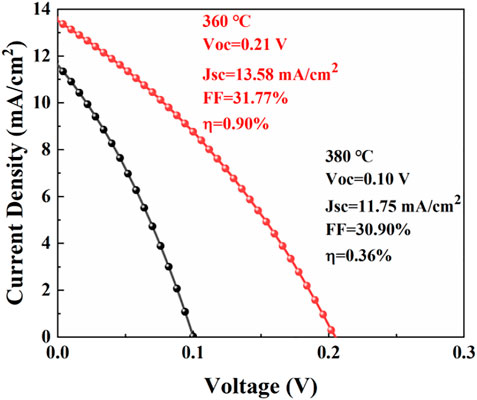
FIGURE 9. J–V curves of the CuSbS2 thin-film solar cells based on absorbers annealed at 360° and 380°C for 30 min.

TABLE 3. Device parameters of the CuSbS2 thin-film solar cells based on absorbers annealed at 360°C and 380°C for 30 min.
Conclusion
In this study, Sb/Cu metal layers were prepared on Mo substrates via the pulse current electrodeposition method. By adjusting the pulse parameters (Ton/Toff of 1:3, a pulse current density of 62.5 mA/cm2, and a pulse current frequency of 10,000 Hz), a compact and uniform Sb layer was prepared on the Mo substrate. With this uniform Sb underlayer, dense, uniform, and smooth Cu layers without dendric clusters were realized. A two-step sulfurization process was employed to fabricate CuSbS2 absorbers. The influences of annealing temperature on the composition, phase, and morphology of CuSbS2 thin films were studied. A compact and relatively pure CuSbS2 thin film was fabricated at 360°C. Finally, a 0.90% efficiency of CuSbS2 thin-film solar cell was obtained with an open-circuit voltage of 0.21 V, a short circuit current density of 13.58 mA/cm2, and an FF of 31.77%.
Data Availability Statement
The original contributions presented in the study are included in the article/Supplementary Material, further inquiries can be directed to the corresponding authors.
Author Contributions
AZ: Conceptualization, Formal analysis, Writing-Original Draft, Writing—Review and Editing. YW: Visualization, Project administration. BL: Data Curation. DX: Data Curation. ZP: Resources. YY: Project administration, Writing-Review and Editing. YX: Data Curation, Project administration. LY: Visualization, Project administration. JB: Validation, Investigation, Writing-Review and Editing, Supervision. WL: Validation, Investigation, Writing-Review and Editing, Supervision.
Funding
This work was supported by the National Natural Science Foundation of China (61804108 and 62074084).
Conflict of Interest
LY was employed by the company Tianjin Institute of Power Source.
The remaining authors declare that the research was conducted in the absence of any commercial or financial relationships that could be construed as a potential conflict of interest.
Publisher’s Note
All claims expressed in this article are solely those of the authors and do not necessarily represent those of their affiliated organizations, or those of the publisher, the editors and the reviewers. Any product that may be evaluated in this article, or claim that may be made by its manufacturer, is not guaranteed or endorsed by the publisher.
Supplementary Material
The Supplementary Material for this article can be found online at: https://www.frontiersin.org/articles/10.3389/fmats.2021.818596/full#supplementary-material
References
Banu, S., Ahn, S. J., Ahn, S. K., Yoon, K., and Cho, A. (2016). Fabrication and Characterization of Cost-Efficient CuSbS2 Thin Film Solar Cells Using Hybrid Inks. Solar Energ. Mater. Solar Cell 151, 14–23. doi:10.1016/j.solmat.2016.02.013
Banu, S., Cho, Y., Kim, K., Ahn, S. K., Gwak, J., and Cho, A. (2019). Phase Transition Behavior and Defect Analysis of CuSbS2 Thin Films for Photovoltaic Application Prepared by Hybrid Inks. Solar Energy 188, 1209–1220. doi:10.1016/j.solener.2019.07.019
Bhattacharya, R. N., Oh, M. K., and Kim, Y. (2012). CIGS-based Solar Cells Prepared from Electrodeposited Precursor Films. Solar Energ. Mater. Solar Cell 98, 198–202. doi:10.1016/j.solmat.2011.10.026
Bi, J., Yao, L., Ao, J., Gao, S., Sun, G., He, Q., et al. (2016). Pulse Electro-Deposition of Copper on Molybdenum for Cu(In,Ga)Se2 and Cu2ZnSnSe4 Solar Cell Applications. J. Power Sourc. 326, 211–219. doi:10.1016/j.jpowsour.2016.07.005
Budevski, E., Staikov, G., and Lorenz, W. J. (2000). Electrocrystallization Nucleation and Growth Phenomena. Electrochim. Acta 45 (15-16), 2559–2574. doi:10.1016/S0013-4686(00)00353-4
Chalapathi, U., Poornaprakash, B., Ahn, C. H., and Park, S. H. (2018). Two-stage Processed CuSbS2 Thin Films for Photovoltaics: Effect of Cu/Sb Ratio. Ceramics Int. 44 (12), 14844–14849. doi:10.1016/j.ceramint.2018.05.117
Colombara, D., Peter, L. M., Rogers, K. D., and Hutchings, K. (2012). Thermochemical and Kinetic Aspects of the Sulfurization of Cu-Sb and Cu-Bi Thin Films. J. Solid State. Chem. 186, 36–46. doi:10.1016/j.jssc.2011.11.025
Colombara, D., Peter, L. M., Rogers, K. D., Painter, J. D., and Roncallo, S. (2011). Formation of CuSbS2 and CuSbSe2 Thin Films via Chalcogenisation of Sb-Cu Metal Precursors. Thin Solid Films 519 (21), 7438–7443. doi:10.1016/j.tsf.2011.01.140
de Souza Lucas, F. W., Welch, A. W., Baranowski, L. L., Dippo, P. C., Hempel, H., Unold, T., et al. (2016). Effects of Thermochemical Treatment on CuSbS2 Photovoltaic Absorber Quality and Solar Cell Reproducibility. J. Phys. Chem. C 120 (33), 18377–18385. doi:10.1021/acs.jpcc.6b04206
Efthimiopoulos, I., Buchan, C., and Wang, Y. (2016). Structural Properties of Sb2S3 under Pressure: Evidence of an Electronic Topological Transition. Sci. Rep. 6, 24246. doi:10.1038/srep24246
Favry, É., Frederich, N., Meunier, A., Omnès, L., Jomard, F., and Etcheberry, A. (2008). Investigation of Organics Adsorption and Inclusion at the Growing Interfaces during the Damascene Process. Electrochimica Acta 53 (23), 7004–7011. doi:10.1016/j.electacta.2008.01.108
Gao, Q., Ao, J., Bi, J., Yao, L., Zhang, Z., Zhang, Y., et al. (2020). A Novel Metal Precursor Structure for Electrodepositing Ultrathin CIGSe Thin-Film Solar Cell with High Efficiency. ACS Appl. Mater. Inter. 12 (21), 24403–24410. doi:10.1021/acsami.0c01008
García, R. G. A., Cerdán-Pasarán, A., Perez, E. A. R., Pal, M., Hernández, M. M., and Mathews, N. R. (2020). Phase Pure CuSbS2 Thin Films by Heat Treatment of Electrodeposited Sb2S3/Cu Layers. J. Solid State. Electrochem. 24 (1), 185–194. doi:10.1007/s10008-019-04475-3
Grujicic, D., and Pesic, B. (2002). Electrodeposition of Copper: the Nucleation Mechanisms. Electrochimica Acta 47 (18), 2901–2912. doi:10.1016/S0013-4686(02)00161-5
Hurma, T., and Kose, S. (2016). XRD Raman Analysis and Optical Properties of CuS Nanostructured Film. Optik 127 (15), 6000–6006. doi:10.1016/j.ijleo.2016.04.019
Kang, L., Zhao, L., Jiang, L., Yan, C., Sun, K., Ng, B. K., et al. (2018). In Situ growth of CuSbS2 Thin Films by Reactive Co-sputtering for Solar Cells. Mater. Sci. Semiconduc Process. 84, 101–106. doi:10.1016/j.mssp.2018.05.004
Kim, S., Yoo, H., Rana, T. R., Enkhbat, T., Han, G., Kim, J., et al. (2018). Effect of Crystal Orientation and Conduction Band Grading of Absorber on Efficiency of Cu(In,Ga)Se2 Solar Cells Grown on Flexible Polyimide Foil at Low Temperature. Adv. Energ. Mater. 8 (26), 1801501. doi:10.1002/aenm.201801501
Kwon, Y. H., Kim, S. K., Kim, S.-W., and Cho, H. K. (2014). Artificially Controlled Two-step Electrodeposition of Cu and Cu/In Metal Precursors with Improved Surface Roughness for Solar Applications. J. Electrochem. Soc. 161 (9), D447–D452. doi:10.1149/2.0771409jes
Lee, S. M., Ikeda, S., Harada, Y. O. T., and Matsumura, M. (2012). Structural Regulation of Electrochemically Deposited Copper Layers for Fabrication of Thin Film Solar Cells with a CuInS2 Photoabsorber. J. Non-Crystalline Sol. 358 (17), 2424–2427. doi:10.1016/j.jnoncrysol.2011.12.043
Lincot, D., Guillemoles, J. F., Taunier, S., Guimard, D., Sicx-Kurdi, J., Chaumont, A., et al. (2004). Chalcopyrite Thin Film Solar Cells by Electrodeposition. Solar Energy 77 (6), 725–737. doi:10.1016/j.solener.2004.05.02410.1016/j.solener.2004.05.024
Long, J. G., Searson, P. C., and Vereecken, P. M. (2006). Electrochemical Characterization of Adsorption-Desorption of the Cuprous-Suppressor-Chloride Complex during Electrodeposition of Copper. J. Electrochem. Soc. 153 (4), C258. doi:10.1149/1.2168050
Loranca-Ramos, F. E., Diliegros-Godines, C. J., Silva González, R., and Pal, M. (2018). Structural, Optical and Electrical Properties of Copper Antimony Sulfide Thin Films Grown by a Citrate-Assisted Single Chemical bath Deposition. Appl. Surf. Sci. 427, 1099–1106. doi:10.1016/j.apsusc.2017.08.027
Macías, C., Lugo, S., Benítez, Á., López, I., Kharissov, B., Vázquez, A., et al. (2017). Thin Film Solar Cell Based on CuSbS 2 Absorber Prepared by Chemical bath Deposition (CBD). Mater. Res. Bull. 87, 161–166. doi:10.1016/j.materresbull.2016.11.028
Medina-Montes, M. I., Campos-González, E., Morales-Luna, M., Sánchez, T. G., Becerril-Silva, M., Mayén-Hernández, S. A., et al. (2018). Development of Phase-Pure CuSbS2 Thin Films by Annealing Thermally Evaporated CuS/Sb2S3 Stacking Layer for Solar Cell Applications. Mater. Sci. Semiconductor Process. 80, 74–84. doi:10.1016/j.mssp.2018.02.029
Mercier, D., Delbos, E., El Belghiti, H., Vigneron, J., Bouttemy, M., and Etcheberry, A. (2013). Study of Copper Electrodeposition Mechanism on Molybdenum Substrate. J. Electrochem. Soc. 160 (12), D3103–D3109. doi:10.1149/2.017312jes
Moffat, T. P., Wheeler, D., Kim, S. K., and Josell, D. (2007). Curvature Enhanced Adsorbate Coverage Mechanism for Bottom-Up Superfilling and Bump Control in Damascene Processing. Electrochimica Acta 53 (1), 145–154. doi:10.1016/j.electacta.2007.03.025
Norkus, E., Vaškelis, A., Jačiauskiene, J., VaičIuniene, J., Gaidamauskas, E., and Macalady, D. L. (2005). Environmentally Friendly Natural Polyhydroxylic Compounds in Electroless Copper Plating Baths: Application of Xylitol, D-Mannitol and D-Sorbitol as Copper(II) Ligands. J. Appl. Electrochem. 35 (1), 41–47. doi:10.1007/s10800-004-2056-7
Oliva, F., Broussillou, C., Annibaliano, M., Frederich, N., Grand, P. P., Roussy, A., et al. (2013). Formation Mechanisms of Cu(In,Ga)Se2 Solar Cells Prepared from Electrodeposited Precursors. Thin Solid Films 535, 127–132. doi:10.1016/j.tsf.2012.11.106
Pal, M., Diliegros‐Godines, C. J., Gupta, G. K., Mathews, N. R., and Dixit, A. (2020). Structural Evolution of Chemically Deposited Binary Stacks of Sb 2 S 3 ‐CuS to Phase‐pure CuSbS 2 Thin Films and Evaluation of Device Parameters of CuSbS 2/CdS Heterojunction. Int. J. Energ. Res. 44 (7), 5881–5894. doi:10.1002/er.5359
Rabhi, A., Kanzari, M., and Rezig, B. (2009). Optical and Structural Properties of CuSbS2 Thin Films Grown by thermal Evaporation Method. Thin Solid Films 517 (7), 2477–2480. doi:10.1016/j.tsf.2008.11.021
Ramos Aquino, J. A., Rodriguez Vela, D. L., Shaji, S., Avellaneda, D. A., and Krishnan, B. (2016). Spray Pyrolysed Thin Films of Copper Antimony Sulfide as Photovoltaic Absorber. Phys. Status Solidi C 13 (1), 24–29. doi:10.1002/pssc.201510102
Riha, S. C., Koegel, A. A., Emery, J. D., Pellin, M. J., and Martinson, A. B. F. (2017). Low-Temperature Atomic Layer Deposition of CuSbS2 for Thin-Film Photovoltaics. ACS Appl. Mater. Inter. 9 (5), 4667–4673. doi:10.1021/acsami.6b13033
Septina, W., Ikeda, S., Iga, Y., Harada, T., and Matsumura, M. (2014). Thin Film Solar Cell Based on CuSbS2 Absorber Fabricated from an Electrochemically Deposited Metal Stack. Thin Solid Films 550, 700–704. doi:10.1016/j.tsf.2013.11.046
van Embden, J., Mendes, J. O., Jasieniak, J. J., Chesman, A. S. R., and Della Gaspera, E. (2020). Solution-Processed CuSbS2 Thin Films and Superstrate Solar Cells with CdS/In2S3 Buffer Layers. ACS Appl. Energ. Mater. 3 (8), 7885–7895. doi:10.1021/acsaem.0c01296
Vauche, L., Risch, L., Sánchez, Y., Dimitrievska, M., Pasquinelli, M., Goislard de Monsabert, T., et al. (2016). 8.2% Pure Selenide Kesterite Thin-Film Solar Cells from Large-Area Electrodeposited Precursors. Prog. Photovolt: Res. Appli. 24 (1), 38–51. doi:10.1002/pip.2643
Vinayakumar, V., Shaji, S., Avellaneda, D. A., Aguilar Martinez, J. A., and Krishnan, B. (2019). Highly Oriented CuSbS2 Thin Films by Rapid thermal Processing of Pre-annealed Sb2S3-Cu Layers for PV Applications. Mater. Sci. Semiconductor Process. 91, 81–89. doi:10.1016/j.mssp.2018.11.007
Vinayakumar, V., Shaji, S., Avellaneda, D., Das Roy, T. K., Castillo, G. A., Martinez, J. A. A., et al. (2017). CuSbS2 Thin Films by Rapid thermal Processing of Sb2S3-Cu Stack Layers for Photovoltaic Application. Solar Energ. Mater. Solar Cell 164, 19–27. doi:10.1016/j.solmat.2017.02.005
Wan, L., Guo, X., Fang, Y., Mao, X., Guo, H., Xu, J., et al. (2019). Spray Pyrolysis Deposited CuSbS2 Absorber Layers for Thin-Film Solar Cells. J. Mater. Sci. Mater. Electron. 30 (24), 21485–21494. doi:10.1007/s10854-019-02531-2
Wan, L., Ma, C., Hu, K., Zhou, R., Mao, X., Pan, S., et al. (2016). Two-stage Co-evaporated CuSbS2 Thin Films for Solar Cells. J. Alloys Comp. 680, 182–190. doi:10.1016/j.jallcom.2016.04.193
Yang, B., Wang, L., Han, J., Zhou, Y., Song, H., Chen, S., et al. (2014). CuSbS2 as a Promising Earth-Abundant Photovoltaic Absorber Material: A Combined Theoretical and Experimental Study. Chem. Mater. 26 (10), 3135–3143. doi:10.1021/cm500516v
Yu, L., Kokenyesi, R. S., Keszler, D. A., and Zunger, A. (2013). Inverse Design of High Absorption Thin-Film Photovoltaic Materials. Adv. Energ. Mater. 3 (1), 43–48. doi:10.1002/aenm.201200538
Yuan, M., Mitzi, D. B., Liu, W., Kellock, A. J., Chey, S. J., and Deline, V. R. (2009). Optimization of CIGS-Based PV Device through Antimony Doping. Chem. Mater. 22 (2), 285–287. doi:10.1021/cm903428f
Zhang, L., Li, Y., Li, X., Li, C., Zhang, R., Delaunay, J. J., et al. (2016). Solution-processed CuSbS2 Thin Film: A Promising Earth-Abundant Photocathode for Efficient Visible-Light-Driven Hydrogen Evolution. Nano Energy 28, 135–142. doi:10.1016/j.nanoen.2016.08.036
Zhang, Y., Huang, J., Yan, C., Sun, K., Cui, X., Liu, F., et al. (2019). High Open-Circuit Voltage CuSbS2 Solar Cells Achieved through the Formation of Epitaxial Growth of CdS/CuSbS2 Hetero-Interface by post-annealing Treatment. Prog. Photovolt Res. Appl. 27 (1), 37–43. doi:10.1002/pip.3061
Keywords: CuSbS2, pulse electrodeposition, Sb/Cu layer, post-sulfurization, thin-film solar cell
Citation: Zhao A, Wang Y, Li B, Xiang D, Peng Z, Yuan Y, Xing Y, Yao L, Bi J and Li W (2022) Sulfurization of Electrodeposited Sb/Cu Precursors for CuSbS2: Potential Absorber Materials for Thin-Film Solar Cells. Front. Mater. 8:818596. doi: 10.3389/fmats.2021.818596
Received: 19 November 2021; Accepted: 06 December 2021;
Published: 05 January 2022.
Edited by:
Xiaotian Wang, Southwest University, ChinaCopyright © 2022 Zhao, Wang, Li, Xiang, Peng, Yuan, Xing, Yao, Bi and Li. This is an open-access article distributed under the terms of the Creative Commons Attribution License (CC BY). The use, distribution or reproduction in other forums is permitted, provided the original author(s) and the copyright owner(s) are credited and that the original publication in this journal is cited, in accordance with accepted academic practice. No use, distribution or reproduction is permitted which does not comply with these terms.
*Correspondence: Jinlian Bi, bijinlian815@126.com; Wei Li, cliwei618@126.com