Characterization of Heavily Irradiated Dielectrics for Pixel Sensors Coupling Insulator Applications
 S. Bharthuar1,2*
  M. Golovleva1,3
  M. Bezak1,3
  E. Brücken1
  A. Gädda1,4 J. Härkönen1,5 A. Karadzhinova-Ferrer1,5 N. Kramarenko1,3
  S. Kirschenmann1,2 P. Koponen1 P. Luukka1,3 K. Mizohata2 J. Ott1,6
  E. Tuominen1,2
- 1Helsinki Institute of Physics, Helsinki, Finland
- 2Department of Physics, University of Helsinki, Helsinki, Finland
- 3Lappeenranta-Lahti University of Technology, Lappeenranta, Finland
- 4Okmetic Oy., Vantaa, Finland
- 5Ludong University, Yantai, China
- 6Aalto University, Department of Electronics and Nanoengineering, Espoo, Finland
An increase in the radiation levels during the high-luminosity operation of the Large Hadron Collider calls for the development of silicon-based pixel detectors that are used for particle tracking and vertex reconstruction. Unlike the conventionally used conductively coupled (DC-coupled) detectors that are prone to an increment in leakage currents due to radiation, capacitively coupled (AC-coupled) detectors are anticipated to be in operation in future collider experiments suitable for tracking purposes. The implementation of AC-coupling to micro-scale pixel sensor areas enables one to provide an enhanced isolation of radiation-induced leakage currents. The motivation of this study is the development of new generation capacitively coupled (AC-coupled) pixel sensors with coupling insulators having good dielectric strength and radiation hardness simultaneously. The AC-coupling insulator thin films were aluminum oxide (Al2O3) and hafnium oxide (HfO2) grown by the atomic layer deposition (ALD) method. A comparison study was performed based on the dielectric material used in MOS, MOSFET, and AC-coupled pixel prototypes processed on high resistivity p-type Magnetic Czochralski silicon (MCz-Si) substrates. Post-irradiation studies with 10 MeV protons up to a fluence of 1015 protons/cm2 suggest HfO2 to be a better candidate as it provides higher sensitivity with negative charge accumulation on irradiation. Furthermore, even though the nature of the dielectric does not affect the electric field within the AC-coupled pixel sensor, samples with HfO2 are comparatively less susceptible to undergo an early breakdown due to irradiation. Edge-transient current technique (e-TCT) measurements show a prominent double-junction effect as expected in heavily irradiated p-type detectors, in accordance with the simulation studies.
1 Introduction
The Phase-2 Upgrade of the LHC to high-luminosity LHC (HL-LHC) in 2027 is expected to increase the instantaneous luminosity by a factor of 5–7, along with a goal of delivering an increase in the integrated luminosity from 400 fb−1 to 3000–4,000 fb−1 (an increase of a factor of ten compared to the expected dataset at that time). During the operation, silicon detector layers within the inner tracker of the CMS experiment will be exposed to increased radiation doses up to 2.3 × 10¹⁶ neq/cm2 (Orfanelli, 2020).
Radiation induced damage within the silicon bulk of the detector leads to trapping of charge carriers, thereby decreasing the charge collection efficiency (CCE) of the detector. However, the detector efficiency can be improved by optimizing the pixel pitch size proportionate to the charge collection length of the detector. Simultaneously, such finely segmented pixel structures provide better position resolution by increasing the granularity of the detector. The CCE of the detector can be improved by reading the signal out due to electrons collected into the n+-implants on p-type silicon as they possess a higher mobility than holes that are collected into the traditional p+-implants on n-type silicon. This consequently has led to the use of silicon detectors with p-type bulk with segmented n+-implants, unlike the traditionally used n-type bulk with segmented p+-implants. However, with the use of silicon dioxide, characteristically a positive oxide charge, the dielectric layer results in surface electron accumulation near the interface of the insulating layer and the p-bulk. This would lead to the formation of a short circuiting channel between the n+-segments, thereby degrading the spatial resolution of the detector. Thus, in order to mitigate this issue, a p-stop or p-spray is usually added to electrically isolate the pixelated segments (Pellegrini et al., 2007). However, this requires additional implantation processing steps which subject the silicon wafers to high temperature and increases the mask levels that reduce the cost-effectiveness of the finally processed detectors.
Alternatively, the segmented implants can be electrically discrete from one another by utilizing thin films of a field insulator with negative oxide charge, such as hafnium oxide (HfO2) and aluminum oxide (Al2O3), for an improved surface current termination strategy. Both Al2O3 and HfO2 have a high negative oxide charge of the order of 1011–1013 cm−2 and possess very good dielectric constants, thereby yielding a higher oxide capacitance (Härkönen et al., 2016a,b).
Thin films of these insulating layers are grown by the atomic layer deposition (ALD) technique. The ALD technique requires low temperatures within 200–300°C and is beneficial in providing very conformal thin films (of tens of nm) with uniform thickness and good accuracy (Suntola, 1992; Leskelä, 2002). ALD HfO2 films are widely used in the contemporary semiconductor industry, specifically for non-volatile memory chips like in portable flash memory storage devices and complementary metal-oxide-semiconductor (CMOS) chips in computers (Müller et al., 2014).
The following study focuses on a comparison of ALD-grown Al2O3 and Al2O3 along with HfO2 (Al2O3 + HfO2) as a field insulator implemented in metal-oxide-semiconductor (MOS) capacitors and field-effect-transistors (MOSFETs) as well as study the robustness in capacitive coupling for n+/p−/p+ pixel detectors, on proton irradiation. An additional layer of HfO2 is incorporated as it possesses a high dielectric constant of a magnitude of 25 (almost 3 times higher than that of Al2O3). This in turn provides a higher capacitive coupling along with a better insulation and improved radiation hardness (Tsui et al., 2013).
2 Measured Device Specifications
The detector fabrication was carried out in the facilities of the Micronova Nanofabrication Centre, Finland’s national research infrastructure for micro- and nanotechnology. The devices were processed on 6-inch boron-doped magnetic Czochralski (MCz) silicon wafers provided by Okmetic Oyj. The wafers have a thickness of 320 μ m and resistivity in the range of 4–8 kΩ-cm. The ion implantation was carried out in an Eaton 8RPP ion implanter, implanting the front side with 60 keV phosphorous ions to target total doses of 1 × 1015 cm−2. The Al2O3 thin films were patterned for finely segmented structures by traditional wet etching, while HfO2 was patterned by chemical mechanical polishing (CMP) into deep reactive ion etching (DRIE) defined structures.
The main samples that were characterized for this study, as shown in Figure 1, are as follows:
• MOS capacitors where the diameter of the gate is 1.5 mm.
• Circular MOSFETs with a channel width of 250 μ m. The source and drains have heavily doped n+-implants where the doping concentration is of a maximum value of 1 × 1019 cm−3. The width of the annular source and the diameter of the circular drain is 200 μ m and 400 μ m, respectively.
• Pad diodes with standard prototype where the active area of the pad is 7.2 × 7.2 mm2.
• AC-coupled pixel sensors similar to the PSI46dig design consisting of 52 × 80 pixel matrix, along with a pitch size of 150 × 100 μ m (Gray, 2013).
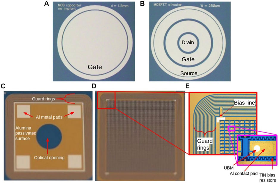
FIGURE 1. Measured samples: (A) MOS capacitor, (B) MOSFET, (C) Pad diode, (D) AC-coupled pixel sensor with metal bias implants, and (E) showing zoomed and detailed structures within the pixel detector.
Detailed information behind the processing of the MOS devices and detectors has been provided in articles—Ott et al. (2020); Gädda et al. (2021); Härkönen et al. (2021); Ott et al. (2021). Each of the abovementioned samples have either Al2O3 or Al2O3 + HfO2 to permit better capacitive coupling. In addition to an improved capacitive coupling layer of individual pixels, thin films of TiN were used as bias resistors in the AC-pixel sensors, as shown in Figure 1E.
The actual thickness of the insulating layer for devices with Al2O3 is 84 nm. On the other hand, the samples employed with Al2O3 + HfO2 as a dielectric layer were of a thickness of 84 and 63 nm, respectively. Since the dielectric constant of HfO2 is almost three times higher than that of Al2O3, the equivalent oxide thickness (defined as the thickness of silicon oxide film that provides the same electrical performance as that of a high dielectric constant material being used) of a composite dielectric system consisting of Al2O3 and HfO2 with thicknesses of 84 and 62 nm, respectively, is reduced by ∼33 nm as compared to 146 nm thick Al2O3. This enables one to achieve similar oxide capacitance values (as can be observed in Section 4.1.1) and simultaneously increase the insulation resistance.
The main aspects of the study associated to the measured samples are as follows:
• First, a comparison study based on the characterization of the devices with either Al2O3 or Al2O3 + HfO2 as a dielectric insulating layer. This is performed by measuring the oxide and oxide–silicon interface charges of pre- and post-irradiated MOS capacitors and MOSFET devices.
• Second, electrical characterization based on current–voltage (I-V), capacitance–voltage (C-V), and e-TCT measurements on AC-coupled pixel sensors with the different dielectrics. Simultaneously, TCAD simulation studies were performed to study the coherence.
The samples were irradiated with 10 MeV protons up to a fluence of 5 ×10¹⁵ protons/cm2. A theoretical value of a magnitude of 3.87 was considered as the NIEL scale factor for silicon.
3 Characterization of Devices
3.1 MOS Capacitors
C-V measurements of a MOS capacitor are performed by measuring the capacitance values with voltage sweep applied across the metal contact, called the gate, as shown in Figure 1A. C-V measurements in MOS capacitors are used to determine the effective oxide and mobile charges of the insulating layer by studying their flat-band voltage. The flat-band voltage is defined as the gate voltage value at which the energy band of the substrate is flat at the silicon and oxide layer interface. In ideal conditions, without any oxide and interface-trapped charges, this value is −0.54 V for MOS devices with aluminum as the metal gate and a silicon substrate with a doping concentration of 8 × 1011 cm−3. The shift in the flat-band voltage (ΔVfb) from its ideal condition gives an estimation of the effective fixed oxide charges (Nf). A fixed oxide charge is a non-ideal condition in MOS capacitors caused by ions which are incorporated in the oxide during growth or deposition (Hu, 2010).
As the MOS capacitors possess a p-type substrate, an accumulation layer is formed when applying a negative bias to the gate due to holes at or near the surface. This surface accumulation condition provides information about the effective fixed oxide charges as the shift in the flat-band voltage from ideal condition (where Vfb ≠ Vgate) corresponds to the maximum capacitance value solely determined by the oxide layer. With positive sweep in the applied gate voltage, the device reaches its flat-band condition and is eventually driven to inversion. Generation of minority charge carriers (electrons in case of p-type substrate) in the inversion region is dependent on the frequency of the measurement. This is due to the difference in the response times of the majority and minority carriers corresponding to the applied voltage. At lower frequencies, the capacitance reaches back to its maximum value for positive gate voltage values due to the formation of the inversion layer by the minority carriers in the oxide–substrate interface. However, at high frequencies, the system is not in thermal equilibrium state where the minority carriers find the sweep rate of the DC gate bias too rapid to follow. Consequently, no inversion layer is formed where a non-equilibrium condition is reached. At this point the neutrality is satisfied when the depletion width gets wider than its value during thermal equilibrium. This results in the lowering of the capacitance value below the saturated thermal equilibrium value, and the device is driven toward deep-depletion condition. Due to this phenomenon, the C-V measurements at a high frequency give rise to an S-shaped curve. All of the MOS capacitors in this study were performed at a high frequency of 1 kHz and an AC signal amplitude of 998.5 mV. The flat-band voltage is experimentally derived by differentiating the (Cmeasured/Coxide)−2 versus bias voltage curve twice. The bias voltage value corresponding to the peak in the double differentiated curve is equal to the flat-band voltage value. Second differentiation usually introduces a great deal of noise as the bias voltage sweeps toward the deep-depletion region but that can be avoided by smoothing the data (Schroder, 2005). The oxide charge density can be determined from the flat-band voltage shift in the C-V curves. A positive value of the effective fixed oxide charge shifts the C-V curve to negative values of applied gate voltages in comparison to ideal C-V curve and vice versa.
In ideal conditions, the flat-band voltage is calculated as the difference in the work function of the metal and substrate. However, on considering the presence of oxide charges in the dielectric layer, the band diagram is modified, as shown in Figure 2. The oxide charge for simplicity is taken to be at the interface of oxide and substrate and induces an electric field with oxide voltage of −Nf/Cox. Consequently, negative oxide in the dielectric changes the flat-band voltage as follows:
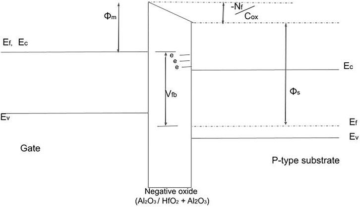
FIGURE 2. Band diagram showing the flat-band condition for MOS capacitors with oxide charge in the oxide–silicon interface.
As Al2O3 and HfO2 are negative oxides, oxide charge Nf shifts the flat-band voltage and consequently the threshold voltage to higher positive values.
The effective fixed oxide charges can be determined using the following relationship:
where Cox is the oxide capacitance corresponding to the accumulation region of the C-V curve. The fixed oxide charge density is further calculated by dividing Nf by the active area of the MOS capacitors.
Another non-ideal condition in MOS capacitors can be noticed due to the mobile charges (Nm) by the hysteresis in the high-frequency capacitance curve when sweeping the gate voltage back and forth from accumulation to inversion region and vice versa (Fowkes and Burgess, 1969). The mobile charges are due to the positive trapped charges induced into the oxide. It has been studied that the origin of mobile ions charges is due to heavy alkaline metallic contamination, like Na+ and K+ ions in case of SiO2 introduced in the oxide layer during the fabrication steps (Repace, 1977; Schroder, 2005; Achuthan, 2007). However, the origin of mobile charges due positive trapped charges in the oxide layer in case of Al2O3 and HfO2 needs further investigation. The shift toward applied voltage in the measured curves differ since a positive gate voltage causes mobile charge to move away from the gate electrode, while a negative voltage attracts the charge toward the gate (Hu, 2010). Therefore, the incorporation of the mobile charges can be used as a factor to determine the sensitivity of the oxide layer in MOS capacitors.
3.2 MOSFET
An increase in the gate voltage (Vg) with positive polarity repels the holes from the surface of the substrate. As a consequence the surface is depleted of mobile charge carriers, and the charge density in the depletion region is dependent on the doping concentration of the substrate. With an increase in Vg, beyond the threshold voltage (Vth), the concentration of conduction electrons increases at the substrate–oxide interface, thereby generating an n-type “inversion” layer at the surface of the substrate. The inversion layer electrons serve as a resistive channel for the current to flow between the highly conductive source to drain regions (Hu, 2010).
Charge built up in the oxides and the silicon–oxide interface of MOS transistors (MOSFETs) due to high-energy ionizing radiation aids in determining the sensitivity of the insulating layer. When exposed to high-energy ionizing radiation, the oxide in MOSFETs generates electron-hole pairs. In our case of p-type substrate MOSFETs, with a positive applied gate bias, most of the electrons and hole pairs that escape recombination advance through the localized states in the oxide and rapidly drift toward the gate and the silicon–oxide interface, respectively. These holes are trapped in the silicon–oxide interface as they “jump” across the localized states within the oxide where they react and form interface traps. It has been studied that due to ionizing irradiation, hydrogen ions are released as holes. The oxide-trapped and interface-trapped charges are studied by determining the threshold voltage (Vth) in drain-to-source current (Ids) versus gate voltage (Vg) characterization at a constant drain-to-source voltage (Vds)—also known as transfer characteristics. The threshold voltage is the point of inflection beyond which Ids increases exponential with gradual increase in Vg. At Vth, interface traps are predominantly positively charged for p-channel transistors and negatively charged for n-channel transistors (Schwank et al., 2008).
The native negative oxide charges and the radiation-induced electron traps in the oxide layer as well as at the interface leads to significant changes in the MOSFET’s channel currents. The channel current is very sensitive to the trapped charges at the interface as they are localized close to the channel. Therefore, the shift in the threshold voltage is a direct measure of the concentration of the charges trapped in the oxide and the interface of the silicon and insulating layer, as mathematically derived in Freeman and Holmes-Siedle (1978).
For measuring the transfer characteristics of the MOSFETs, the samples are placed on a chuck which is in contact to its backplane. The chuck is grounded virtually with a 0 Ω resistor. There are three needles, each connected to the gate, source, and drain, respectively. The needles are held by the micro-manipulator which helps in making the metallic contacts and guard rings by moving them in three dimensions ( − x, − y and − z directions) by the help of fine adjustment screws. The needle in contact with the gate is used to apply bias voltage with the help of a DC power supply (with a voltage range of ±200 V). The other two needles connected to the source and drain are grounded with 0 Ω resistor and Keithley 6487 picoampere meter, respectively. Keithley 6487 is used to measure the drain-to-source current (Ids). It consists of a voltage source which is completely isolated from the electrometer. This enables us to measure the Ids (with sweeping Vg) by simultaneously setting the drain-to-source voltage (Vds) fixed at a constant value. Output characteristics of the MOSFETs were recorded by measuring the variation in Ids with sweeping Vds for specific Vg values. This in turn will enable us in determining the threshold voltage, identified as the gate voltage value beyond which the device is no longer operating in the cut-off region.
3.3 Diodes and Pixel Detectors
The radiation hardness studies of AC-coupled pixel sensors without any implanted bias lines were performed using C-V and TCT methods. The full depletion voltage and the silicon bulk capacitance after full depletion were determined using C-V measurements on pre- and post-irradiated AC-coupled pixel sensors containing Al2O3 or Al2O3 + HfO2 as the dielectric insulating material. Based on C-V measurements, the full depletion voltage of the detector is identified as the bias voltage beyond which the capacitance is constant. The value is extracted by determining the inflection point in inverse-square capacitance versus bias voltage (1/C2-V) plot. The effective doping concentration (Neff) value of the detector substrate is determined from the full depletion voltage (Vfd) by using the following relation:
where ϵ0 and ϵSi are the permittivities of the vacuum and silicon, respectively, and W is the substrate thickness. Furthermore, the resistivity (ρ) of silicon substrate can be calculated from the effective doping concentration and charge carrier mobility, using the following relation:
where μh is the hole mobility as the detectors possess a p-type substrate.
For C-V characterization of the sensors and MOS capacitors, we used the LCR meter E4980A with a test frequency range from 20 Hz to 1 MHz to measure capacitance with an accuracy of 1 fF. Due to the technical limitations of this setup, only high-frequency C-V curves at 1 kHz were taken into consideration during the measurements. The device has a maximum signal voltage level of 1 V. The bias voltage is provided to backplane with help of a Keithley 2410C sourcemeter that can provide voltage within the range of ±1000 V. The voltage source has a maximum current of 1 mA and can also measure higher currents which is useful in case of irradiated samples. There are two needles, one connected to the bias line in case of pixel detectors or the metal contact pad in diodes from where the capacitance is measured, while the other is connected to the innermost guard ring of the sensor which is grounded. A detailed schematic and explanation of the setup has been described in Arsenovich (2020).
The variation in total dark leakage current densities, leakage current damage factor (α), electric field, and charge collection efficiency (CCE), due to irradiation, were measured using the TCT characterization method. TCT is a method commonly used for electrical characterization of semiconductor detectors. In TCT, a fast pulsed infrared (IR) laser is used to imitate the crossing of minimum ionizing particles (MIPs) through the detector. The photons of IR laser traversing through the depleted region within the bulk generate charge carriers and provide a better approximation of high-energy particles interacting with the detector. These carriers (electrons and holes) traverse from the generation point within the bulk toward their respective electrodes. The resulting transient signal induced by the movement of the charge carriers in an electric field, according to the Shockley–Ramo theorem, is detected by the oscilloscope. The shape of the signal is studied to analyze the electric field, doping concentration, and the charge collection efficiency of the detector. The collected charge at a given bias voltage is calculated by integrating the current signal over time. On performing a voltage sweep at a given position on the sensor optically exposed to the laser beam, the saturation of the collected charge beyond a certain bias can be interpreted as the onset of full depletion of the sensor (Eremin et al., 1996; Fretwurst et al., 1997; Mandić et al., 2015, 2013, 2014).
The measurements in this study were performed with a Particulars d.o.o. (Ljubljana, Slovenia) based scanning-TCT setup. An IR laser (1,064 nm) directed either toward the front side plane or the edge of the sensor was used. The laser pulse was transmitted to the detector by an optical fiber. The signal was identified in areas without any metal as the photons could pass through the active depleted region and generate the charge carriers. The measurements were performed at a low IR laser intensity of 60%, equivalent to the charge deposition of 5–10 MIPs and repetition rate of 1 kHz. The reverse bias voltage is applied to the backplane of the sensor, while the transient signal is read from the front bias line of the pixel sensor with the n+-implant. The first guard ring surrounding the bias line is grounded with a 50 Ω terminator. In addition to the IR laser, the other components in the measurement setup were focusing optics, a sample holder mounted on a XYZ stage for scanning the entire surface of the detector, a Keithley 2410C 1100 V Sourcemeter unit, bias tee, a wide band current amplifier with a Tenma power supply, and a LeCroy WaveRunner 8404M-MS 4 GHz oscilloscope. During the measurement campaign, an average of more than 100 waveforms was recorded at each scanning point by the oscilloscope. An offset correction for the onset time and baseline was applied to all measurements. Figure 3A shows a schematic view of the electronic connections during the measurement.
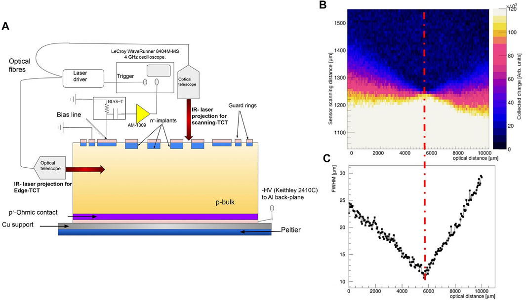
FIGURE 3. (A) Schematic view of the TCT experimental setup (not to scale). Based on focus-scan performed by using the “knife-edge” technique (B) shows that the focused beam spot of the IR laser beam is at a distance of 5,850 μ m with respect to the edge of sensor and (C) the size (FWHM) of the laser spot at this focused position is of a magnitude of 12 μ m.
The collected charge and the depletion width of the detector can be studied by projecting the IR laser beam across the edge of the detector, also known as the edge-TCT (e-TCT) characterization method. Figure 3A portrays a layout for the characterization of the sensor using e-TCT as well. The focus spot of the Gaussian laser beam is determined by using the “knife-edge” technique (Khosrofian and Garetz, 1983; de Araújo et al., 2009). As shown in Figure 3C, the beam size is ∼12 μ m. The corresponding position of the focused beam spot was calculated to be at a distance of 5,680 μ m with respect to the edge of the active region of the sensor, as shown in Figure 3B. The depth profile is calculated by recording the current signals as the laser scans across the depth of the sensor.
Furthermore, the electric field within the active region of the depleted bulk of the detector can be determined by producing the drift velocity profiles while scanning the IR laser beam across the depth of the detector. The induced current signal generated initially due to the charge carriers is given by the following expression:
Furthermore, on expressing the drift velocity to mobility, we get the following relationship:
Therefore, the drift velocity can be predicted by integrating over the initial rise time of the current signal. The signal rise time is ∼ 300 ps, which is of the same order of magnitude as the trapping time for detectors irradiated at a fluence of 1015 protons/cm2. Therefore, as the maximum drift distance of the charge carriers at 300 ps is ≈ 30 μ m, which is comparable to size of the beam, the drift velocity profiles were calculated by integrating over 300 ps of the signal rise time. This is also known as the prompt current method (Canali et al., 1971).
As shown in Eq. 6, the drift velocity can be expressed in terms of an electric field and mobility, where according to our approximation the mobility of the charge carriers is constant across their drift length. In cases where the drift velocity has not saturated as function of electric field strength, the sum of the drift velocities (of both electrons and holes) gives an image of the electric field strength within the sensor. Studies have been performed under the RD50 collaboration at CERN to investigate the carrier mobility dependence on fluence by magnetoresistance means. Results show an inverse-square root dependence of mobility on fluence values beyond a magnitude of 1 × 10¹⁴ neq/cm2, for low electric fields. However, for high electric fields, the variation of carrier mobility does not change that significantly with fluence, except for heavily irradiated sensors beyond 1 × 10¹⁵ neq/cm2. The total mobility of the charge carriers decreases by ∼ 20% on irradiating silicon detectors from 1 × 10¹⁴ to 1 × 10¹⁵ neq/cm2, depending on the concentration of cluster defects in the bulk (Vaitkus et al., 2021). However, the variation in the mobility of the charge carriers with an electric field has not been taken into consideration to simplify the model for our measurements.
Furthermore, in order to cross-check the investigations of the electric field distribution with simulation, a larger 2-D structure was created. The simulated sensor configurations were designed with parameters as close to the real sensors as possible. The sensor had a physical thickness of 320 μ m, a pitch of 150 μ m, and a pixel implant width of 100 μ m. The doping concentration of the p-type bulk was set to 8 × 1011 cm−3. In addition to that the heavily phosphorus-doped silicon implants in the front and boron implantation on the backplane had peak concentrations of a magnitude of 1 × 1015 cm−3 and 5 × 1015 cm−3, respectively. Each pixel had a biasing electrode as well as AC-coupled charge collecting contacts. The reverse bias voltage was provided to the backplane Ohmic contact at room temperature.
4 Results
4.1 Proton-Irradiated MOS Capacitors and MOSFETs
4.1.1 C-V Measurements of MOS Capacitors
C-V curves for MOS capacitors with different oxides are shown in Figures 4A,B. The curves were recorded by sweeping the gate voltage from accumulation to inversion, that is, starting from negative to positive values as the devices possess a p-type substrate and vice versa. As explained earlier, the hysteresis in the C-V curve for each sample helps in analyzing the concentration of mobile charges in the insulating layer. The results show no significant hysteresis in voltage sweep for non-irradiated sample. However, a shift in the flat-band condition voltage (Vfb) from ideal conditions (where Vfb = −0.54 V for MOS devices with aluminum as the metal gate and a silicon substrate with a doping concentration of 8 × 1011 cm−3) is observed in the non-irradiated MOS capacitors, irrespective of the nature of the oxide layer. Nevertheless, MOS capacitors with a combination of Al2O3 + HfO2 as the oxide layer possess a Vfb shift of (2.18 ± 0.35) V lower than those with Al2O3 as the dielectric layer. This corresponds to a decrease in the fixed oxide charges by a factor of ∼ 1.5 for samples with HfO2, as shown in Figure 5A. The fixed oxide charge increases by a factor of ∼ 3 with irradiation and this is observed as a positive shift in the flat-band voltage. The physics behind this can be explained as a consequence of increasing negative charge accumulation at the oxide–silicon interface that causes the bands to be pulled down farther in equilibrium. In order to achieve the flat-band condition, one must apply a positive voltage to overcome the inherent bending of the bands. A negative charge in the oxide near the p-type silicon substrate aids in increasing the holes on the surface, so the gate voltage required to invert the surface to become n-type is increased, as a consequence of which, this behavior will lead to shifts in the threshold voltage as well to higher positive values.
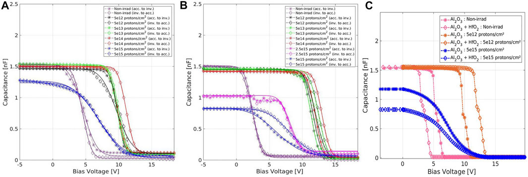
FIGURE 4. C-V plots for pre- and post-irradiated MOS capacitors with (A) Al2O3 and (B) Al2O3 + HfO2 as the dielectric layer, measured at a frequency of 1 kHz. (C) TCAD simulated C-V plots for pre- and post-irradiated MOS capacitors with different oxide layers.
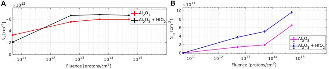
FIGURE 5. Evolution of effective (A) fixed charges (Nf) and (B) mobile charges (Nm) in proton-irradiated MOS capacitors with different insulating layers.
No hysteresis for non-irradiated MOS capacitors was observed, thereby inferring that there are no positive heavy alkaline ions induced in the oxide layer due to contamination during the fabrication steps. However, the hysteresis observed for irradiated samples is possibly due to the mobile charges originating from radiation-induced traps. Furthermore, the effective mobile charge increases on irradiation of the MOS capacitors to a fluence of 5 × 10¹⁴ protons/cm2. The value is by a factor of ∼ 1.6 higher in case of samples possessing Al2O3 + HfO2 in comparison to those consisting of Al2O3 alone, as shown in Figure 5B. This shows that MOS capacitors with HfO2 show higher sensitivity to irradiation.
The simulated MOS capacitor structure had dimensions of 1 × A × 320 μ m3, where A is the area factor to match the dimensions with the real device. The thicknesses of the Al2O3 and HfO2 as the insulating layer for the devices were identical to the fabricated samples. The bulk doping concentration was set to 6 × 1011 cm−3. The Vfb shift due to irradiation can be assessed from measurements, as shown in Figure 4C, and it is directly assigned to an amount of oxide charge density (Qox) increase at the oxide–silicon interface. These variables are then used as input parameters for the TCAD surface damage model. The oxide–silicon interface is also characterized by interface traps distributed throughout the silicon energy gap. From a macroscopic point of view, it is represented as a stretch out in the high-frequency capacitance–voltage curve. The interface trap states density Dit can be estimated by means of the capacitance high-low method (Nicollian and Brews, 1982). Due to the technical limitations in low-frequency measurements and inaccuracies at extremely high-frequency, C-V curves for MOS capacitors were obtained at only 1 kHz. Therefore, the Dit was found by fitting simulated C-V curves to the measurement results. The interface states were modeled with two single trap levels, one donor at 0.50 eV from the valence band edge (EV) and one acceptor at 0.50 eV from the conduction band edge (EC). All the parameters that were used for the surface damage model are listed in the Table 1.
TABLE 1. Details of the surface damage model.
It is evident from Figure 4C that for the first radiation fluence step there is only an increase in the effective oxide charge with no change in the interface trap concentration. However, for the highest fluence dose, an increase in the interface trap concentration occurs. The simulation adds evidence to the fact that the interface traps play an important role for higher fluences.
4.1.2 Output and Transfer Characteristics of MOSFETs
Radiation-induced threshold voltage shift due to charges trapped in the gate oxide as well as the oxide–silicon interface is dependent on the irradiation dose that the MOSFET device is exposed to. The total shift in the threshold voltage (ΔVth) is the sum of the threshold voltage shifts due to oxide trap (ΔVot) and interface trap charge (ΔVit) as shown below:
The cumulative shift in the threshold voltage depends on the increase in oxide-trapped charges (Not) and interface-trapped charges (Nit), given by the following equation:
where Cox is the oxide capacitance in the accumulation region retrieved from C-V measurement.
The generation of dangling bonds in the oxide–silicon interface due to irradiation is responsible for predominantly trapping holes as they hop across the localized states in the oxide where they react and form the interface traps. An increase in the interface-trapped charges decreases the channel mobility. As a consequence of the deep hole trapping, a high amount of negative charge gets accumulated in the interface forming the interface traps in the n-channel MOS. On the other hand, defects in the oxide generated by radiation lead to trapping of negative charge, thereby causing an increase in applied gate voltage value to reach threshold condition. At high radiation doses to 5 × 10¹⁴ protons/cm2, the concentration of oxide traps supersedes the interface charges causing a positive shift in threshold voltage, as shown in Figure 6A.
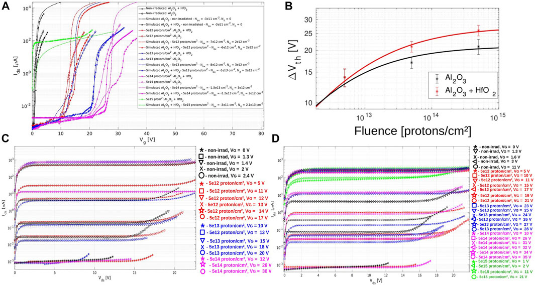
FIGURE 6. (A) Measured and TCAD simulated transfer characteristics and variation of drain-source current (Ids) with gate voltage (Vg) for pre- and post–proton-irradiated MOSFETs with different dielectrics, at a constant drain-to-source voltage of 1 V.(B) Change in the shift in threshold voltage (ΔVth) with fluence for proton-irradiated MOSFETs with different oxides. Output characteristics and variation of Ids with Vds, measured at varying Vg values for non-irradiated and irradiated MOSFETs with (C) Al2O3 and (D) Al2O3 + HfO2 as the dielectric layer.
TCAD simulation was performed on pre- and post-irradiated MOSFETs with alumina and hafnia as the dielectric layer to cross-check the transfer characteristics. The simulated MOSFET structure had dimensions similar to the specifications provided in Section 2. The doping concentration and the energy level parameters were similar to that of the MOS capacitors, as listed in Table 1. The results are congruous to the measurements where the shift in the threshold voltage to higher bias values is due to the cumulative contribution of negative oxide and interface-trapped charges. Up to a fluence of 5 × 10¹⁴ protons/cm2, the oxide-trapped charges supersede the interface traps, giving rise to a positive shift in the threshold voltage. However, at fluences above 5 × 10¹⁴ protons/cm2, the concentration of the interface-trapped charges exceeds that of the oxide traps causing a huge increase in the leakage current (by ∼ 4 orders of magnitude) as well as a slightly negative shift in the threshold voltage that can potentially cause a breakdown of the chip (Lho and Kim, 2005). Therefore, as shown in Figure 6B, the variation in the effective threshold voltage with fluence was taken into account for samples with different dielectric layers irradiated to a fluence of 5 × 10¹⁴ protons/cm2. The threshold voltage value can be extracted by determining the x-axis coordinate of the intersection point for the two linear fits which correspond to the inflection point in each of the Ids versus Vg curves, shown in Figure 6A, for pre- and post–proton-irradiated MOSFETs with different dielectrics.
The cumulative shift in the oxide and interface-trapped charges, Δ(Not/Nit) as in Figure 7A, increases by a factor of ∼5 when irradiated to a fluence of 5 × 10¹⁴ protons/cm2. As the devices operate in low-field regimes, the following curve was utilized to fit in the ΔVth versus fluence plot:
where D is the proton fluence and (a, b, c) are three curve-fit parameters. The boundary conditions are defined such that for non-irradiated samples when D is zero ΔVth is also zero. Furthermore, when fluence goes to infinity, a saturates to its maximum value corresponding to no further change in threshold voltage at the maximum fluence of proton irradiation. The value of parameter a extracted from the fit was five times higher for samples with Al2O3 + HfO2 as the dielectric layer.
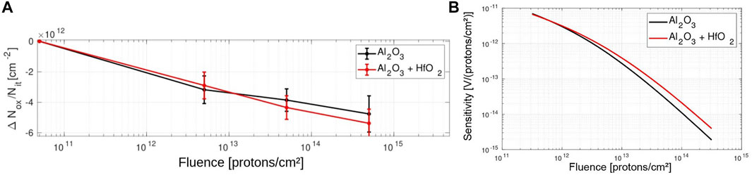
FIGURE 7. (A) Variation in the cumulative concentration of oxide and interface-trapped charges and (B) sensitivity with fluence for proton-irradiated MOSFET samples with Al2O3 and Al2O3 + HfO2 in the oxide layer.
The sensitivity (ratio of the change in threshold voltage to fluence) was calculated by using the parameters extracted from the fits for the different samples based on the nature of the dielectrics employed in MOSFETs. As shown in Figure 7B, MOSFETs with additional layer of HfO2 show higher sensitivity to proton irradiation at high fluences. This is expected for MOSFETs with high-k dielectric materials (Yilmaz et al., 2008; Kaya et al., 2015; Kaya et al., 2018).
Furthermore, the output characteristics, as shown in Figures 6C,D, for MOSFETs with Al2O3 and Al2O3 + HfO2 as dielectric layers, respectively, validate the reproduciblity of the results in extraction of threshold voltage from transfer characteristics. The MOSFET is in the cut-off region for gate voltage values below the threshold voltage where the current is way too low (in nA scale) and the device is in off-state. At gate voltage values above the threshold value, Ids values beyond the linear/ohmic region remain constant before undergoing breakdown. This operation region where Ids remains constant with increasing Vds is called the saturation region. It is important to note that for Vg
4.2 Proton-Irradiated AC-Coupled Pixel Sensors
4.2.1 I-V/C-V Measurements
Figure 8A shows the variation in the total leakage current for PIN-diode–like structures irradiated up to a fluence of 1015 protons/cm2, measured at a temperature of − 15°C after annealing at room temperature for a day. Furthermore, the parameter damage factor (α) can be calculated with respect to the total leakage current of non-irradiated samples by using the formula from Moll (1999)
where the terms Φeq and V represent the fluence for proton irradiation and volume of the diode, respectively. The average value of α for fully depleted diodes irradiated up to a fluence of 1015 is (4.55 ± 0.65) × 10–17 A/cm (Wiehe et al., 2018).
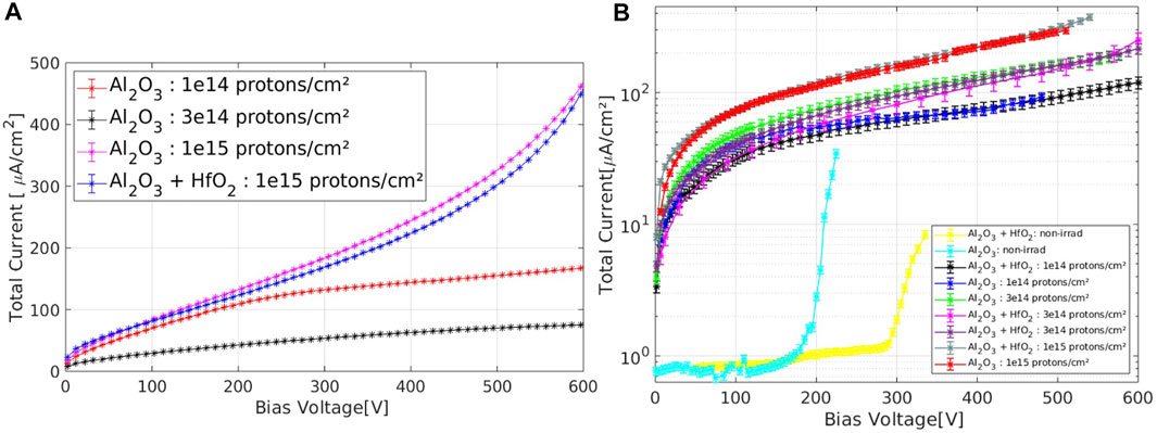
FIGURE 8. (A) Variation in the total leakage current based on the I-V characterization of PIN diode sensors irradiated up to a fluence of 1015 protons/cm2. (B) Total leakage current of pre- and post-irradiated pixel sensors versus bias voltage for AC-coupled pixel sensors with different dielectric layers measured at −15°C.
The total leakage current of the non-irradiated and irradiated AC-coupled pixel sensors with different dielectric layers, measured at a temperature of −15°C, is shown in Figure 8B. For non-irradiated sensors, the reverse bias total leakage current increases proportionally to the square root of the bias voltage until the detector breaks down beyond which the dark current rises more sharply. It is a characteristic feature of the non-irradiated pixel sensors to possess an early breakdown (Dieter et al., 2021). The possible reason for an early breakdown is due to the formation of an Ohmic current path along the detector surface resulting in the loss of electrical isolation between the pixels. The major difference is that samples with HfO2 can sustain high bias voltages as it provides better insulation than sensors with Al2O3 alone as a dielectric layer. Non-irradiated pixel sensors with HfO2 as an insulating layer have a maximum operational voltage, approximately 100 V higher. With irradiation up to a fluence of 1015 protons/cm2, results show that the sensors with Al2O3 + HfO2 as an insulating layer are able to sustain a higher electric field, and there is no breakdown visible up to the maximum test operational voltage of approximately 550 V.
The inflection point in the inverse-square capacitance versus bias voltage curves from the C-V measurements at room temperature, as shown in Figure 9A, provides the full depletion voltage of the detector. The increasing shift in the full depletion voltage with an increasing fluence of proton irradiation is irrespective of the nature of the insulating layer. It is important to note that full depletion voltage of the active bulk is attainable in case of pixel sensors with Al2O3 + HfO2 as the oxide layer since they were able to sustain a high bias voltage without undergoing an early breakdown. The full depletion voltage of the active bulk of the detector, using Eq. 4, for non-irradiated sensors is approximately 76 V which corresponds to a doping concentration value of 1.08 × 1012 cm−3 and a resistivity of 12 kΩ cm. The resistivity of the fully depleted bulk based on the C-V measurements is increased by a factor of ∼ 1.5 in comparison to the specifications of the wafers provided by Okmetic. The reason behind this observation is related to the thermal donors induced due to the oxygen diffusion in the magnetic Czochralski-grown silicon ingots along with additional heating that the wafer is subjected to during the detector processing steps (Tuovinen et al., 2007). Furthermore, with irradiation, as shown in Figure 9B, the full depletion voltage of the sensors irradiated up to a fluence of 1015 protons/cm2 increases up to (570 ± 15) V. This corresponds to an increase in the doping concentration by factor of ∼7 and decrease in the resistivity of the fully depleted bulk to approximately 2 kΩ-cm.
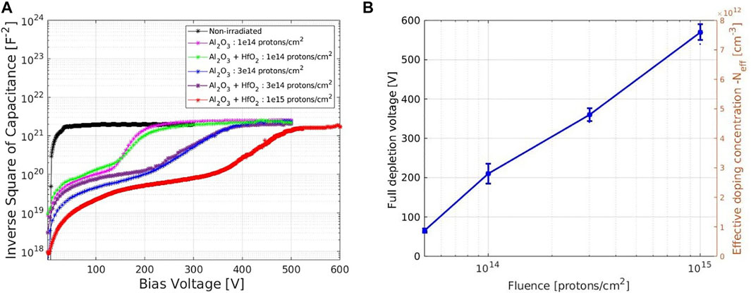
FIGURE 9. (A) Inverse-square capacitance versus bias voltage curves for AC-coupled pixel sensors with Al2O3 + HfO2 used as the dielectric layer irradiated up to a fluence of 1015 protons/cm2. (B) Variation in the full depletion voltage and the corresponding doping concentration of fully depleted bulk of proton-irradiated AC-coupled pixel sensors with fluence.
Also, unlike for the non-irradiated sensors, the inverse-square capacitance versus voltage curves for irradiated AC-coupled pixel sensors, as shown in Figure 9A, are non-linearly increasing before the full depletion of their bulk (Sato et al., 2020). This implies that the effective bulk resistivity after irradiation is not uniform along the depth of the detector due to trapping of charge carriers released by the generation current in the radiation-induced defects. Consequently, it results in space charge sign inversion of the detector close to the backplane of the sensor, thereby leading to a “double-junction” effect (Hara et al., 2016), explained in Section 4.2.2.
4.2.2 TCT Measurements
Front illumination of IR laser in TCT characterization of AC-coupled pixel sensors aids in studying the homogeneity in the collected charge spatially across the active region of the detectors. Figure 10A shows the mask layout of the scanned area for a non-irradiated pixel sensor with metallic bias line consisting of Al2O3 + HfO2 as the dielectric layer in the detector. An area of 2.7 × 1.7 mm2 was scanned with IR laser at a laser intensity corresponding to charge deposited by approximately ∼ 10 MIPs at a bias voltage of 280 V and a constant temperature of −15°C. The total dark current during the measurement at the corresponding bias was 12.15 μ A. Figure 10B shows the spatial homogeneity in the charge collected across the scanned area within the active region of the sensor. The region of minimum collected charge, according to the color scale, corresponds to the metallized region of the detectors, that is, the pixels, the bias lines, and the guard rings. The region of maximum collected charge corresponds to the spaces in the sensor without any metallization as the IR laser photons can pass through the bulk of the detector to generate the signal due to charge carriers collected by the electrodes. Since only the first guard ring is terminated with a 50 Ω resistor and the subsequent guard rings are left floating, a gradient in the collected charge can be observed in the scans from the innermost to the outer guard rings. This ensures a gradual gradient in the potential as the voltage drops from outside in Evensen et al. (1993).
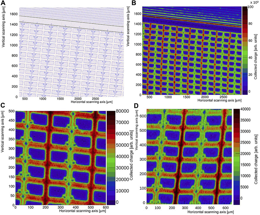
FIGURE 10. Validation showing (A) the mask layout of an area of 2,700 × 1700 μ m2 of a non-irradiated AC-coupled sensor with metallic bias line and (B) its corresponding charge collection spatial homogeneity scan. Spatial homogeneity scans performed at a bias of 300 V with front illumination of IR laser showing a scanned area of (C) 500 × 600 μ m2 for 1014 protons/cm2 and (D) 620 × 650 μ m2 for 1015 protons/cm2 irradiated AC-coupled pixel sensors with Al2O3 + HfO2 used as the dielectric layer.
Figures 10C,D show a spatial scan of two pixel sensors, with Al2O3 + HfO2 as the insulating layer, irradiated at 1014 protons/cm2 and 1015 protons/cm2. They were measured at a constant bias of 300 V and subjected with IR laser of the same intensity as for the non-irradiated sample. Results show that on proton irradiation, the resolution of the pixels based on the collected charge homogeneity scans does not change significantly. However, the maximum collected charge within the active region of the sensor is reduced by a factor of 2.25 (approximately 55%) and 1.13 (approximately 11%) for samples irradiated at fluences of 1015 protons/cm2 and 1014 protons/cm2, respectively. The reduction in the value of the collected charge is due to trapping of charge carriers in defect states within the bandgap of silicon (Oblakowska-Mucha, 2017). The reason for the traps is associated to the dislocation of the silicon atoms from its lattice site to an interstitial site leading to a displacement damage in the cascade of multiple interactions, thereby causing cluster defects (Lindström, 2003).
The full depletion voltage can be determined from the inflection point in the variation in a collected charge versus bias voltage plots for non-irradiated and irradiated sensors, as shown in Figure 11. The CCE for non-irradiated sensors does not depend on the nature of the employed insulating layer. The full depletion voltage of the non-irradiated pixel sensor extracted from the front illumination of IR laser in TCT measurement is of a magnitude of ∼75 V, similar to the value extracted from the C-V measurements in Figure 9. As observed earlier in the spatial homogeneity scans for irradiated samples, the collected charge is reduced approximately by factor of 1.11, 1.27, and 2.1 for pixel sensors irradiated at fluences of 1014, 3 ×10¹⁴, and 1015 protons/cm2, respectively. The corresponding full depletion voltages extracted from the “knee” point was identified to be of a magnitude of 197 and 344 V for sensors irradiated at fluences of 1014 and 3 ×10¹⁴ protons/cm2, respectively. However, the inflection point in the curve could not be identified for 1015 protons/cm2 irradiated sample as the source measure unit (SMU) reached compliance at a bias of 492 V due to high reverse leakage current values.
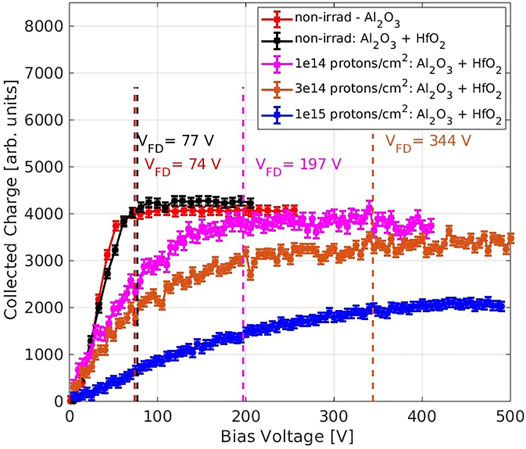
FIGURE 11. Variation in collected charge versus bias voltage sweep from the front IR laser illumination TCT characterization method for non-irradiated and irradiated pixel sensors at varying proton fluences, measured at − 15°C.
Based on illumination of IR laser across the edge of the detector, e-TCT aids in evaluating the charge collection and electric field profiles by analyzing the drift velocity of the generated charge carriers across the active bulk of the sensor, as shown in the relation in Eq.5. The amplitude and shape of the waveforms recorded by the oscilloscope vary depending on the position at which the IR laser is projected across the edge of the sensor, as shown in Figure 12A. In reverse bias conditions, when the laser beam is pointed at a distance of 30 μ m from the surface of the sensor, the electrons drift quickly toward the electrodes close to the segmented n+ implants as in case of silicon the electron mobility is ∼ 3 times higher than hole mobility. The generated electrons are collected rapidly close to the front surface electrodes and contribute toward the rise time of the signal peak. Meanwhile, the holes traverse through the entire bulk and are collected toward the electrode on the backplane of the sensor and give rise to the transient current signal, detected by the oscilloscope, as the movement of charge induced in an electric field is in accordance with the Shockley–Ramo theorem (Shockley, 1938; Ramo, 1939). Furthermore, charge carriers generated due to the projection of the IR laser beam within the bulk, ∼190 μ m from the surface of the sensor, drift toward their respective electrodes giving rise to a Gaussian signal. The negative polarity is a consequence of reflections due to impedance mismatching between the bias tee and the detector (Kramberger et al., 2010).
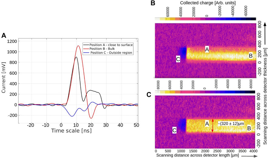
FIGURE 12. (A) Signal waveforms readout when IR laser is projected at different positions across the edge of the detector.(B,C) showing the 2-dimensional collected charge mappings on integrating over 15 and 40 ns of the current signal, respectively, as the IR laser scans across the active thickness of the detector. The measurement was performed at a constant bias voltage of 120 V at room temperature.
Figures 12B,C show the homogeneity in the collected charge mapping for a non-irradiated pixel sensor at a constant bias voltage of 120 V at room temperature by integrating the current signal over 15 and 40 ns, respectively. Integrating the signal over a timescale of 40 ns gives an estimation of the bulk thickness with a magnitude of (320 ± 12) μ m. The uncertainty of 12 μ m is arising from the size of the Gaussian laser beam. The e-TCT collected charge scans were performed over a length of 2.7 mm within the active region of the sensor along with one of its ends consisting of the guard rings. A gradient in the negative collected charge corresponding to the negative signal can be observed within the region under the guard rings in the spatially scanned maps. The first guard ring that is grounded contributes to the negative signal with a low amplitude due to the generated holes which charge and discharge the active region (similar to that of a capacitor) as they share the common ohmic backplane from where the sensor is biased (Bharthuar et al., 2020). However, no signal was detected beyond 2.7 mm (toward the right side of the plot) of the scanning length of the sensor as the HV bias line attached to the spring connector of the readout board blocked the laser beam from reaching the sensor.
Charge collection profiles at different bias voltages for non-irradiated pixel sensors with different dielectrics, as can be seen in Figures 13A,B, show no difference depending on the nature of the dielectric material implemented in the detector. The magnitude of the normalized charge collection value saturates to a maximum amplitude of ∼1 throughout the active bulk of the sensor at bias voltage values beyond 75 V. Therefore, the active bulk of the pixel sensors with a thickness of ∼320 μ m is fully depleted at a bias voltage of 75 V.
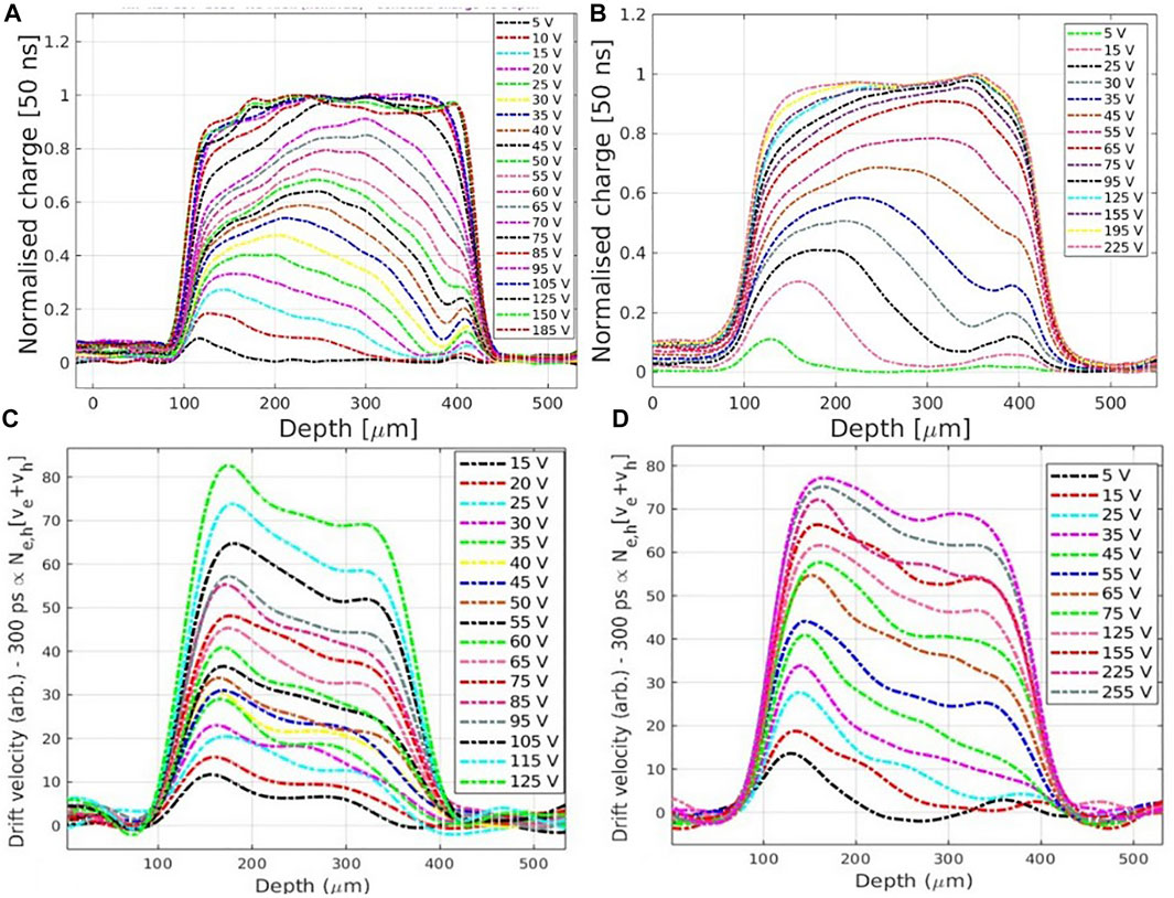
FIGURE 13. Normalized collected charge versus depth profiles at varying bias voltages for non-irradiated AC-coupled pixel sensors with (A) Al2O3 and (B) Al2O3 + HfO2 as the insulating layer, measured at room temperature. Drift velocity profiles at varying bias voltages for non-irradiated sensors with (C) Al2O3 and (D) Al2O3 + HfO2 as the insulating layer, measured at room temperature.
For voltage values above the full depletion voltage, the total charge collected at any point across the thickness of the sensor does not depend on the position of the electron-hole pair generation. At voltage values below the full depletion voltage, the regions around the pixels are more efficient owing to the depletion growth from the segmented n+-implants side. Meanwhile, at bias greater than full depletion voltage, the pixelated side of the sensor is less efficient than the backplane due to the long drift of the holes and is consequently ballistic deficit. As the detector begins to deplete, a thin depleted region is formed due to the difference in the doping concentration between the p-bulk and p++-Ohmic contact. As a result of this, a double-junction is observed in the charge collection profiles for low bias voltages. The non-vanishing normalized charge value is observed beyond the active thickness of the detector as a consequence of light reflection from the support plate (Kramberger et al., 2010; Kramberger et al., 2014).
The electric field can be numerically determined from Eq. 5 by extracting the drift velocity profiles using the prompt method, as shown in Figures 13C,D, for non-irradiated sensors with different dielectrics. An almost uniform gradient in the electric field profiles is observed with a maximum at a depth beyond 30 μ m from the segmented side and a gradual minimum toward the backplane of the sensor. A low electric field is initially measured close to the segmented implants/pixels. This is due to the small velocity dependence on the electric field at a field strength of approximately 1 V/μ m and also the fact that the electric field calculated at a specific position across the depth of the sensor is an average over the pixel width and the laser beam diameter. The profile reaches its peak at a depth beyond ∼30 μ m as the current signal due to the electrons and holes is integrated over a time approximately equivalent to this distance on account of the bandwidth limitations of the amplifier and the oscilloscope. No significant difference in the electric field profiles is observed depending on the nature of the dielectric material employed in the pixel sensors.
The pixel sensor irradiated to a fluence of 1014 protons/cm2 was fully depleted at a bias of 175 V. The full depletion voltage extracted in the charge collection profiles in Figure 14A is slightly lower (by approximately 20 V) than the value calculated from C-V measurements. At bias values above the full depletion voltage, the charge collection profiles remain almost constant with no further increase in the maximum collected charge value at any point across the active thickness of the sensor. A uniform charge collection profile is unattainable for a sensor irradiated to a fluence of 3 × 10¹⁴ protons/cm2, although it is depleted at a bias of 350 V. This corresponds to the reason that the field strength is not strong enough for the release of the charge carriers from the traps. However, a sharp gradient in the charge collection profiles is observed in sensors irradiated at 1015 protons/cm2 due to the increase in the trapping effects. The transition between active and non-active region can be seen in Figures 14B,C as a steep fall of the collected charge along the depth of the sensor. The active region grows with an increase in the bias voltage and is caused by an increase in the amount of weighting potential crossed by the charge carriers. The weighting potential spreads across the entire thickness of the high resistivity bulk even though the sensor is not fully depleted. Some charge increases slightly at depths above ∼240 μ m due to the “double-peak effect” (Menichelli et al., 1999).
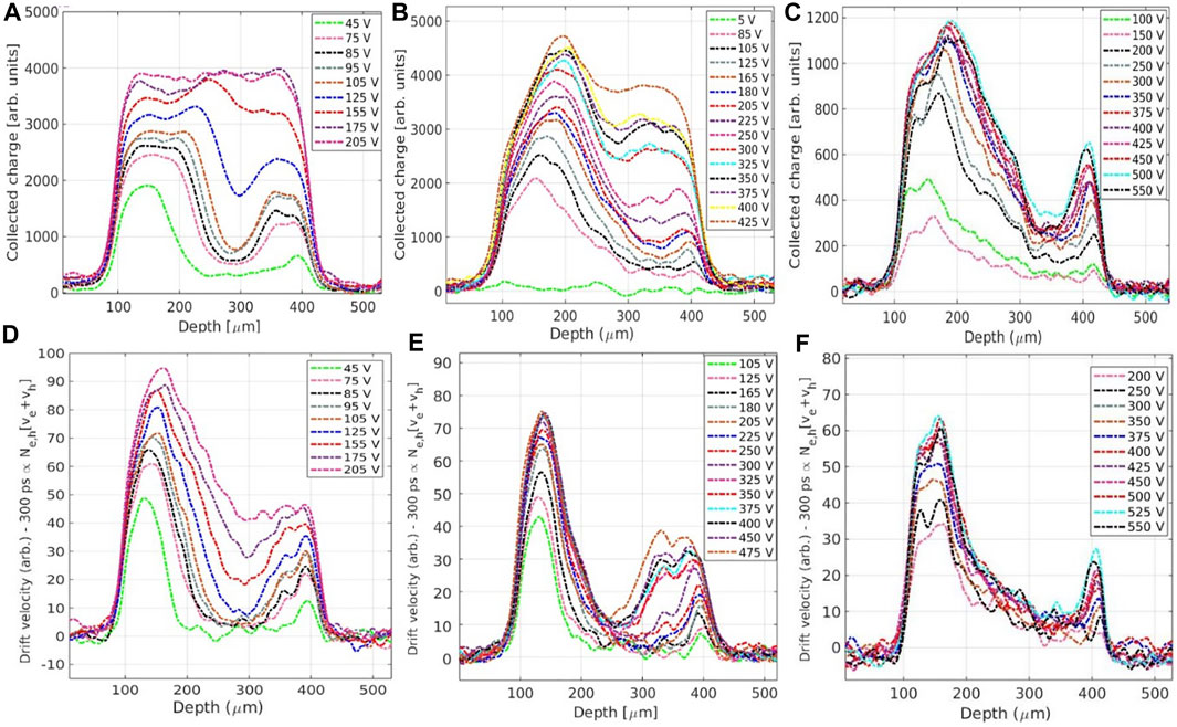
FIGURE 14. Measured charge collection profiles at varying bias voltages for AC-coupled pixel sensor irradiated to a fluence of: (A) 1014 protons/cm2, (B) 3 × 10¹⁴ protons/cm2, and (C) 1015 protons/cm2, at a temperature of −15°C.(D–F) Electric field profiles for the AC-coupled pixel sensors irradiated with the same fluences, respectively.
Furthermore, with irradiation, the electric field near the backplane of the sensor gets much weaker than the junction close to the pixels, as shown in Figures 14D–F , which indicates that the contribution of induced charge carriers drifting toward the backplane is less significant. This gives rise to the characteristic double-peak distortion in the electric field that gets more prominent for sensors irradiated to fluences above 1014 protons/cm2. The reason behind this effect is due to deep-level traps of non-uniform concentration of charge carriers originating from radiation-induced defects (Eremin et al., 2004; Castaldini et al., 2002). As can be noticed in Figure 14D, for a pixel sensor irradiated at 1014 protons/cm2, the double-junction effect gets less pronounced for higher bias voltages as the MCz-silicon wafers possess a high concentration of oxygen of a magnitude of ∼1017 cm−3 responsible for the suppression of deep-level traps formations by decreasing the mid-gap defect concentrations (Verbitskaya et al., 2007).
In the simulation, the bulk damage is approximated by an effective two-defect model with the parameters listed in Table 2. Surface damage is modeled in the simulation by placing a fixed charge at the oxide–Si interface and the interface traps that were assessed from the MOS capacitor simulation. The simulated electric field profiles for sensors irradiated at 2, 4, 10, and 20 × 1014 protons/cm2, as shown in Figure 15, exhibit a similar double-peak effect that gets more pronounced for heavily irradiated samples above 2 × 10¹⁴ protons/cm2. This concurs with results from the two-defect model as shown in Eremin et al. (2002).
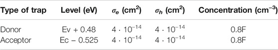
TABLE 2. Details of the two-level bulk damage model F is the fluence in neq/cm2.
FIGURE 15. Sentaurus TCAD–based simulation plot showing the variation in the electric field profile across the active bulk of an irradiated p-type silicon detector at different fluences biased at 150 V, using the Eremin model.
The pulse amplitude and width is affected with irradiation. In case the electron-hole pairs are generated close to the pixels, majority of the induced charge is a consequence of holes drifting toward the backplane of the sensor. With irradiation, the signal amplitude and width get much shorter, clearly evident in the comparison between sensors irradiated to fluences of 3 × 10¹⁴ and 1015 protons/cm2, as shown in Figures 16B,C, respectively. This is a consequence of high drift velocities and increases trapping effects. However, with an increase in the bias voltage, the width and the amplitude of the pulse increased due to the increase in the depletion width of the detector.
FIGURE 16. Induced current pulses at varying depths for pixel sensors with Al2O3 + HfO2 as the dielectric layer irradiated to (A) 1014 protons/cm2, (B) 3 × 10¹⁴ protons/cm2, and (C) 1015 protons/cm2 are measured at constant temperature of −15°C and bias voltage values of 120 V, 245, and 250 V, respectively.
The pixel sensor irradiated to 1014 protons/cm2 possesses shorter induced current signals due to charge carriers generated close to the pixels. However, with an increase in the depth, the peak of the signal is shifted (delayed) by a few hundreds of picoseconds corresponding to the time needed for the electrons to drift to the segmented electrodes. For heavily irradiated sensors, irradiated above 1014 protons/cm2, the second peak in the signal gets more prominent at high bias voltages of 250 V, especially when the position of the laser beam moves away from the pixels. The reason for the second peak in the induced current pulses is mainly due to the drift of the holes generated as a consequence of the avalanche multiplication of the electrons in the region of the high electric field near the segmented implants/pixels (Kramberger et al., 2014).
5 Conclusion
Characterization of MOS and MOSFET devices indicates a negative charge accumulation is induced by proton irradiation based on the study of the flat-band voltage and shift in the threshold voltage, respectively. The negative oxide charge during the irradiation is an essential prerequisite of radiation hardness resiliency of n+/p−/p+(n on p) particle detectors widely intended to be used in future high-luminosity experiments. MOS devices with Al2O3 + HfO2 possess higher sensitivity to irradiation, especially when irradiated to high fluences, in comparison to samples with Al2O3 alone as the oxide layer. Furthermore, at fluences above 5 × 10¹⁴ protons/cm2, an increase in the concentration of the interface-trapped charges leads to negative shift in threshold and a subsequent increase in the leakage current.
Studies based on e-TCT measurements suggest that the impact of different dielectric–silicon interfaces show hardly any differences on the functionality of the AC-pixel sensors. However, the double-junction effect as a consequence of deep-level traps in the bandgap of silicon was identified in proton-irradiated samples. The double-junction effect gets more prominent for sensors irradiated to higher fluencies. This is congruous to the simulation studies using the two-defect model for proton-irradiated sensors.
Data Availability Statement
The raw data supporting the conclusion of this article will be made available by the authors, without undue reservation.
Author Contributions
All authors listed have made a substantial, direct, and intellectual contribution to the work and approved it for publication.
Funding
The research is supported by the Magnus Ehrnrooth Foundation (research grant number 200 011). This study was partially funded by the Academy of Finland (project number 314 473), “Multi-spectral photon-counting for medical imaging and beam characterization.”
Conflict of Interest
Author AG was employed by the company Okmetic Oy.
The remaining authors declare that the research was conducted in the absence of any commercial or financial relationships that could be construed as a potential conflict of interest.
Publisher’s Note
All claims expressed in this article are solely those of the authors and do not necessarily represent those of their affiliated organizations, or those of the publisher, the editors, and the reviewers. Any product that may be evaluated in this article, or claim that may be made by its manufacturer, is not guaranteed or endorsed by the publisher.
Acknowledgments
SB would like to acknowledge the Magnus Ehrnrooth Foundation for financial support. Facilities for detector fabrication were provided by Micronova Nanofabrication Centre in Espoo, Finland within the OtaNano research infrastructure. The proton irradiation of the samples was performed at the Accelerator Laboratory in University of Helsinki. The C-V, I-V, and TCT measurements were performed at the Detector Laboratory in Helsinki Institute of Physics. The authors are grateful for Mr. Jaakko Salonen’s assistance in CMP processing.
References
Arsenovich, T. (2020). Reliability and Quality Assurance Methods for Silicon Detectors and Their Application to the Development of Detectors with Alumina Thin Films. Helsinki, Finland: Helsinki Univ. Ph.D. thesis.
Bharthuar, S., Ott, J., Helariutta, K., Litichevskyi, V., Brücken, E., Gädda, A., et al. (2020). Study of Interpad-gap of HPK 3.1 Production LGADs with Transient Current Technique. Nucl. Instr. Methods Phys. Res. Section A: Acc. Spectrometers, Detectors Associated Equipment 979, 164494. doi:10.1016/j.nima.2020.164494
Canali, C., Ottaviani, G., and Alberigi Quaranta, A. (1971). Drift Velocity of Electrons and Holes and Associated Anisotropic Effects in Silicon. J. Phys. Chem. Sol. 32, 1707–1720. doi:10.1016/S0022-3697(71)80137-3
Castaldini, A., Cavallini, A., Polenta, L., Nava, F., and Canali, C. (2002). Electric Field Distribution in Irradiated Silicon Detectors. Nucl. Instr. Methods Phys. Res. Section A: Acc. Spectrometers, Detectors Associated Equipment 476, 550–555. doi:10.1016/S0168-9002(01)01655-2
de Araújo, M. A., Silva, R., de Lima, E., Pereira, D. P., and de Oliveira, P. C. (2009). Measurement of Gaussian Laser Beam Radius Using the Knife-Edge Technique: Improvement on Data Analysis. Appl. Opt. 48, 393. doi:10.1364/AO.48.000393
Dieter, Y., Daas, M., Dingfelder, J., Hemperek, T., Hügging, F., Janssen, J., et al. (2021). Radiation Tolerant, Thin, Passive CMOS Sensors Read Out with the RD53A Chip. Nucl. Inst. Methods. Phys. Res. A 1015, 165771. doi:10.1016/j.nima.2021.165771
Eremin, V., Li, Z., Roe, S., Ruggiero, G., and Verbitskaya, E. (2004). Double Peak Electric Field Distortion in Heavily Irradiated Silicon Strip Detectors. Nucl. Instr. Methods Phys. Res. Section A: Acc. Spectrometers, Detectors Associated Equipment 535, 622–631. doi:10.1016/j.nima.2004.06.14310.1016/s0168-9002(04)01462-7
Eremin, V., Strokan, N., Verbitskaya, E., and Li, Z. (1996). Development of Transient Current and Charge Techniques for the Measurement of Effective Net Concentration of Ionized Charges (Neff) in the Space Charge Region of P-N junction Detectors. Nucl. Instr. Methods Phys. Res. Section A: Acc. Spectrometers, Detectors Associated Equipment 372, 388–398. doi:10.1016/0168-9002(95)01295-8
Eremin, V., Verbitskaya, E., and Li, Z. (2002). The Origin of Double Peak Electric Field Distribution in Heavily Irradiated Silicon Detectors. Nucl. Instr. Methods Phys. Res. Section A: Acc. Spectrometers, Detectors Associated Equipment 476, 556–564. doi:10.1016/S0168-9002(01)01642-4
Evensen, L., Hanneborg, A., Avset, B. S., and Nese, M. (1993). Guard Ring Design for High Voltage Operation of Silicon Detectors. Nucl. Instr. Methods Phys. Res. Section A: Acc. Spectrometers, Detectors Associated Equipment 337, 44–52. doi:10.1016/0168-9002(93)91136-B
Fowkes, F. M., and Burgess, T. E. (1969). Electric fields at the Surface and Interface of SiO2 Films on Silicon. Surf. Sci. 13, 184–195. doi:10.1016/0039-6028(69)90247-7
Freeman, R., and Holmes-Siedle, A. (1978). A Simple Model for Predicting Radiation Effects in MOS Devices. IEEE Trans. Nucl. Sci. 25, 1216–1225. doi:10.1109/TNS.1978.4329516
Fretwurst, E., Eremin, V., Feick, H., Gerhardt, J., Li, Z., and Lindström, G. (1997). Investigation of Damage-Induced Defects in Silicon by TCT. Nucl. Instr. Methods Phys. Res. Section A: Acc. Spectrometers, Detectors Associated Equipment 388, 356–360. doi:10.1016/S0168-9002(97)00002-8
Gädda, A., Ott, J., Bharthuar, S., Brücken, E., Kalliokoski, M., Karadzhinova-Ferrer, A., et al. (2021). AC-coupled N-In-P Pixel Detectors on MCz Silicon with Atomic Layer Deposition (ALD) Grown Thin Film. Nucl. Instr. Methods Phys. Res. Section A: Acc. Spectrometers, Detectors Associated Equipment 986, 164714. doi:10.1016/j.nima.2020.164714
Gray, J. A. (2013). The CMS Phase-1 Pixel Detector. J. Inst. 8, C12047. doi:10.1088/1748-0221/8/12/C12047
Hara, K., Allport, P. P., Baca, M., Broughton, J., Chisholm, A., Nikolopoulos, K., et al. (2016). Charge Collection and Field Profile Studies of Heavily Irradiated Strip Sensors for the ATLAS Inner Tracker Upgrade. Nucl. Instr. Methods Phys. Res. A 831, 181–188. doi:10.1016/j.nima.2016.04.035
Härkönen, J., Ott, J., Gädda, A., Bezak, M., Brücken, E., Tuovinen, E., et al. (2021). Processing and Interconnections of Finely Segmented Semiconductor Pixel Detectors for Applications in Particle Physics and Photon Detection. Front. Phys. 9, 32. doi:10.3389/fphy.2021.601730
Härkönen, J., Ott, J., Mäkelä, M., Arsenovich, T., Gädda, A., Peltola, T., et al. (2016b). Atomic Layer Deposition (ALD) Grown Thin Films for Ultra-fine Pitch Pixel Detectors. Nucl. Instr. Methods Phys. Res. Section A: Acc. Spectrometers, Detectors Associated Equipment 831, 2–6. doi:10.1016/j.nima.2016.03.037
Härkönen, J., Tuovinen, E., Luukka, P., Gädda, A., Mäenpää, T., Tuominen, E., et al. (2016a). Processing of N+/p−/p+ Strip Detectors with Atomic Layer Deposition (ALD) Grown Al2O3 Field Insulator on Magnetic Czochralski Silicon (MCz-Si) Substrates. Nucl. Instr. Methods Phys. Res. Section A: Acc. Spectrometers, Detectors Associated Equipment 828, 46–51. doi:10.1016/j.nima.2016.04.069
Hu, C. (2010). Modern Semiconductor Devices for Integrated Circuits. New Jersey: Pearson/Prentice Hall.
Kaya, S., Jaksic, A., Duane, R., Vasovic, N., and Yilmaz, E. (2018). FET-based Radiation Sensors with Er 2 O 3 Gate Dielectric. Nucl. Instr. Methods Phys. Res. Section B: Beam Interactions Mater. Atoms 430, 36–41. doi:10.1016/j.nimb.2018.06.007
Kaya, S., Yilmaz, E., Kahraman, A., and Karacali, H. (2015). Frequency Dependent Gamma-ray Irradiation Response of Sm2O3 MOS Capacitors. Nucl. Instr. Methods Phys. Res. Section B: Beam Interactions Mater. Atoms 358, 188–193. doi:10.1016/j.nimb.2015.06.037
Khosrofian, J. M., and Garetz, B. A. (1983). Measurement of a Gaussian Laser Beam Diameter through the Direct Inversion of Knife-Edge Data. Appl. Opt. 22, 3406–3410. doi:10.1364/AO.22.003406
Kramberger, G., Cindro, V., Mandić, I., Mikuž, M., Milovanović, M., and Zavrtanik, M. (2014). Modeling of Electric Field in Silicon Micro-strip Detectors Irradiated with Neutrons and Pions. J. Inst. 9, P10016. doi:10.1088/1748-0221/9/10/p10016
Kramberger, G., Cindro, V., Mandic, I., Mikuz, M., Milovanovic, M., Zavrtanik, M., et al. (2010). Investigation of Irradiated Silicon Detectors by Edge-TCT. IEEE Trans. Nucl. Sci. 57, 2294–2302. doi:10.1109/TNS.2010.2051957
Leskelä, M. (2002). Atomic Layer Deposition (ALD): from Precursors to Thin Film Structures. Thin Solid Films 409, 138–146. doi:10.1016/S0040-6090(02)00117-7
Lho, Y. H., and Kim, K. Y. (2005). Radiation Effects on the Power Mosfet for Space Applications. Etri J. 27, 449–452. doi:10.4218/etrij.05.0205.0031
Lindström, G. (2003). Radiation Damage in Silicon Detectors. Nucl. Instr. Methods Phys. Res. A 512, 30–43. doi:10.1016/S0168-9002(03)01874-6
Mandić, I., Cindro, V., Gorišek, A., Kramberger, G., Mikuž, M., Milovanović, M., et al. (2013). TCT Measurements of Irradiated Strip Detectors with a Focused Laser Beam. J. Inst. 8, P04016. doi:10.1088/1748-0221/8/04/P04016
Mandić, I., Cindro, V., Gorišek, A., Kramberger, G., Mikuž, M., and Zavrtanik, M. (2015). Edge-TCT Measurements with the Laser Beam Directed Parallel to the Strips. J. Inst. 10, P08004. doi:10.1088/1748-0221/10/08/P08004
Mandić, I., Cindro, V., Gorišek, A., Kramberger, G., Mikuž, M., Zavrtanik, M., et al. (2014). TCT Measurements with Slim Edge Strip Detectors. Nucl. Instr. Methods Phys. Res. Section A: Acc. Spectrometers, Detectors Associated Equipment 751, 41–47. doi:10.1016/j.nima.2014.03.026
Menichelli, D., Bruzzi, M., Li, Z., and Eremin, V. (1999). Modelling of Observed Double-junction Effect. Nucl. Instr. Methods Phys. Res. Section A: Acc. Spectrometers, Detectors Associated Equipment 426, 135–139. doi:10.1016/S0168-9002(98)01482-X
Moll, M. (1999). Radiation Damage in Silicon Particle Detectors: Microscopic Defects and Macroscopic Properties. Hamburg, Germany: Hamburg Univ. Ph.D. thesis.
Müller, J., Polakowski, P., Müller, S., and Mikolajick, T. (2014). (Invited) Ferroelectric Hafnium Oxide Based Materials and Devices: Assessment of Current Status and Future Prospects. ECS Trans. 64, 159. doi:10.1149/06408.0159ecst
Nicollian, E. H., and Brews, J. R. (1982). MOS /metal Oxide Semiconductor/Physics and Technology. John Wiley & Sons, Inc.
Oblakowska-Mucha, A. (2017). Radiation Damage in Silicon Particle Detectors in High Luminosity Experiments. Acta Phys. Pol. B 48, 1707. doi:10.5506/APhysPolB.48.1707
Orfanelli, S. (2020). The Phase 2 Upgrade of the CMS Inner Tracker. Nucl. Instr. Methods Phys. Res. Section A: Acc. Spectrometers, Detectors Associated Equipment 980, 164396. doi:10.1016/j.nima.2020.164396
Ott, J., Bharthuar, S., Gädda, A., Arsenovich, T., Bezak, M., Brücken, E., et al. (2021). Characterization of Magnetic Czochralski Silicon Devices with Aluminium Oxide Field Insulator: Effect of Oxygen Precursor on Electrical Properties and Radiation Hardness. J. Inst. 16, P05011. doi:10.1088/1748-0221/16/05/P05011
Ott, J., Gädda, A., Bharthuar, S., Brücken, E., Golovleva, M., Härkönen, J., et al. (2020). Processing of AC-Coupled N-In-P Pixel Detectors on MCz Silicon Using Atomic Layer Deposited Aluminium Oxide. Nucl. Instr. Methods Phys. Res. Section A: Acc. Spectrometers, Detectors Associated Equipment 958, 162547. doi:10.1016/j.nima.2019.162547
Pellegrini, G., Fleta, C., Campabadal, F., Miñano, M., Lozano, M., Rafí, J. M., et al. (2007). Technology of P-type Microstrip Detectors with Radiation Hard p-spray, P-Stop and Moderated P-spray Insulations. Nucl. Instr. Methods Phys. Res. Section A: Acc. Spectrometers, Detectors Associated Equipment 579, 599–603. doi:10.1016/j.nima.2007.05.253
Ramo, S. (1939). Currents Induced by Electron Motion. Proc. IRE 27, 584–585. doi:10.1109/jrproc.1939.228757
Repace, J. L. (1977). Radiation-Induced Increase of Mobile Sodium in MOS Capacitors. IEEE Trans. Nucl. Sci. 24, 2088–2092. doi:10.1109/TNS.1977.4329170
Sato, K., Hara, K., Onaru, K., Harada, D., Wada, S., Ikegami, Y., et al. (2020). Characteristics of Silicon Strip Sensor Irradiated up to a Proton Fluence of 1017neq∕cm2. Nucl. Instr. Methods Phys. Res. Section A: Acc. Spectrometers, Detectors Associated Equipment 982, 164507. doi:10.1016/j.nima.2020.164507
Schroder, D. K. (2005). Semiconductor Material and Device Characterization. 3rd Edition. John Wiley & Sons, Inc.
Schwank, J. R., Shaneyfelt, M. R., Fleetwood, D. M., Felix, J. A., Dodd, P. E., Paillet, P., et al. (2008). Radiation Effects in Mos Oxides. IEEE Trans. Nucl. Sci. 55, 1833–1853. doi:10.1109/TNS.2008.2001040
Shockley, W. (1938). Currents to Conductors Induced by a Moving Point Charge. J. Appl. Phys. 9, 635–636. doi:10.1063/1.1710367
Suntola, T. (1992). Atomic Layer Epitaxy. Thin Solid Films 216, 84–89. doi:10.1016/0040-6090(92)90874-B
Tsui, B.-Y., Su, T.-T., Shew, B.-Y., and Huang, Y.-T. (2013). Effect of Surface Preparation on the Radiation Hardness of High-Dielectric Constant Gate Dielectric. Solid-State Elect. 81, 119–123. doi:10.1016/j.sse.2012.11.010
Tuovinen, E., Härkönen, J., Luukka, P., and Tuominen, E. (2007). Intentional thermal Donor Activation in Magnetic Czochralski Silicon. Mater. Sci. Semiconductor Process. 10, 179–184. doi:10.1016/j.mssp.2007.11.006
Vaitkus, J. V., Mekys, A., and Vaitekonis, Š. (2021). Electron Mobility Dependence on Neutron Irradiation Fluence in Heavily Irradiated Silicon. physics 61, 1216–1225. doi:10.3952/physics.v61i2.4438
Verbitskaya, E., Eremin, V., Li, Z., Härkönen, J., and Bruzzi, M. (2007). Concept of Double Peak Electric Field Distribution in the Development of Radiation Hard Silicon Detectors. Nucl. Instr. Methods Phys. Res. Section A: Acc. Spectrometers, Detectors Associated Equipment 583, 77–86. doi:10.1016/j.nima.2007.08.228
Wiehe, M., Wonsak, S., Kuehn, S., Parzefall, U., and Casse, G. (2018). Measurements of the Reverse Current of Highly Irradiated Silicon Sensors to Determine the Effective Energy and Current Related Damage Rate. Nucl. Instr. Methods Phys. Res. Section A: Acc. Spectrometers, Detectors Associated Equipment 877, 51–55. doi:10.1016/j.nima.2017.09.021
Keywords: AC-pixel sensors, MOS capacitor, MOSFET, radiation hardness, alumina, hafnia, ALD (atomic layer deposition), magnetic Czochralski
Citation: Bharthuar S, Golovleva M, Bezak M, Brücken E, Gädda A, Härkönen J, Karadzhinova-Ferrer A, Kramarenko N, Kirschenmann S, Koponen P, Luukka P, Mizohata K, Ott J and Tuominen E (2022) Characterization of Heavily Irradiated Dielectrics for Pixel Sensors Coupling Insulator Applications. Front. Mater. 8:769947. doi: 10.3389/fmats.2021.769947
Received: 02 September 2021; Accepted: 16 December 2021;
Published: 19 January 2022.
Edited by:
Wenzhuo Wu, Purdue University, United StatesReviewed by:
Dana Weinstein, Purdue University, United StatesJackson Anderson, Purdue University, United States, in collaboration with reviewer DW
Sharaf Sumaiya, Intel, United States
Copyright © 2022 Bharthuar, Golovleva, Bezak, Brücken, Gädda, Härkönen, Karadzhinova-Ferrer, Kramarenko, Kirschenmann, Koponen, Luukka, Mizohata, Ott and Tuominen. This is an open-access article distributed under the terms of the Creative Commons Attribution License (CC BY). The use, distribution or reproduction in other forums is permitted, provided the original author(s) and the copyright owner(s) are credited and that the original publication in this journal is cited, in accordance with accepted academic practice. No use, distribution or reproduction is permitted which does not comply with these terms.
*Correspondence: S. Bharthuar, shudhashil.bharthuar@helsinki.fi