Ultrafast Broadband Nonlinear Optical Response in Co-Doped Sb2Se3 Nanofilms at Near-Infrared
 Di Sun1
  Yu Fang
 Wenjun Sun
- 1School of Physics and Electrical Engineering, Harbin Normal University, Harbin, China
- 2School of Mathematics and Physics, Suzhou University of Science and Technology, Suzhou, China
- 3Department of Physics, Harbin Institute of Technology, Harbin, China
- 4Key Laboratory of Photonic and Electric Bandgap Materials, Ministry of Education, School of Physics and Electronic Engineering, Harbin Normal University, Harbin, China
Transition metal-doped Sb2Se3 has become a heated topic caused by the strong nonlinear optical response and the ultrafast response time at high laser excitation. In this paper, the Co-doped Sb2Se3 with different doping amount (0.5, 1.0, and 1.5 W) nanofilms were prepared by magnetron sputtering technology, and the nonlinear behavior of Co-doped Sb2Se3 nanofilms at near infrared were systematically studied. The results of the femtosecond Z-Scan experiment indicate that the Co-doped Sb2Se3 nanofilms exhibit broadband nonlinear response properties owing to the free carrier absorption, the Kerr refraction, the two-photon absorption, and the free carrier refraction. The nonlinear absorption coefficients of Co-doped Sb2Se3 nanofilms are from 3.0 × 10⁻⁹ to 2.03 × 10⁻⁸ m/ W under excitation at 800, 980, and 1,030 nm, and the nonlinear refractive index of the Co-doped Sb2Se3 nanofilms is from 4.0 × 10⁻¹⁶ to -3.89 × 10⁻¹⁵ m2/ W at 800, 980, and 1,030 nm. More importantly, Co-doped Sb2Se3 (1.5 W) nanofilm exhibits ultrafast carrier absorption (<1 ps) and a stronger transient absorption intensity of ΔOD > 6.3. The Co-doping content can controllably tune the crystalline degree, the ultrafast carrier absorption, the intensity of the reverse saturation absorption, the broadband nonlinear optical response, and the carrier relaxation time of Co-doped Sb2Se3 nanofilms. These results are sufficient to support their applications in broadband nonlinear photonic devices.
Introduction
The special interactions between light and matter in selenide materials are ideal applications for interferometers, electrocatalysis, ultrathin transistors, sensors, and optoelectronic devices (Radisavljevic and Kis, 2013; Medina et al., 2017; Ai et al., 2018; Jiang et al., 2019). In nonlinear optics, the selenides, due to their unique reverse saturation absorption (RSA), which decreases transmittance with the incident laser increase, have attracted much attention (Wang et al., 2012; Lin et al., 2013). The RSA behavior occurs because the absorption cross-section of the excited state in the substance is larger than the ground state, which leads to the ground state absorption being less than that of the excited state (Henari and Dakhel, 2011; Tuhl et al., 2012). The RSA properties of selenides can be widely used in optical information, nonlinear optoelectronic components, optical sensing, and integrated optics (Djordjevic and Arabaci, 2010; Volz et al., 2012; Jia et al., 2018). For example, WSe2 in selenides exhibits RSA and optical limiting properties that can be applied to nonlinear optoelectronic components (Major et al., 2004; Andreev et al., 2011). However, the selenides with RSA properties still face the solution of the ultrafast broadband nonlinear optical response, higher carrier absorption intensity, long carrier relaxation time, and other problems.
In past decades, researchers have focused on Sb2Se3 (V–VI group), which is widely used in optical devices due to its excellent optical nonlinear properties (Molli et al., 2016; Liu et al., 2019). To further improve the photoelectric properties of Sb2Se3, the group IV, VII, and VI elements are frequently doped on Sb2Se3 (Choi et al., 2006; Lee et al., 2019; Ren et al., 2020). A variety of metal elements have been selected for doping with Sb2Se3 due to their excellent photoelectric properties (Cao et al., 2014; Ning et al., 2021). In many metal elements, Co was selected to dope the Sb2Se3 because it can effectively capture the photogenerated carrier and promote free-carrier absorption (FCA) at near infrared. The success of Co doping can effectively adjust the optical bandgap and accelerate the FCA and two-photon absorption (TPA) of Sb2Se3, making the nonlinear response transfer to the broadband. It is of great significance for the selection of a greater metal dopant to doped Sb2Se3 for nonlinear optical devices and electronic devices due to understanding the doping effect and nonlinear properties of Co-doped Sb2Se3.
In this paper, the pure and Co-doped Sb2Se3 nanofilms with different contents of Co dopant (0.5, 1.0, and 1.5 W) nanofilms were successfully prepared by using magnetron sputtering technology. The Co-doped Sb2Se3 (1.5 W) nanofilm exhibits an excellent ultrafast broadband nonlinear response at the near infrared, higher nonlinear absorption coefficients, higher transient absorption intensity, ultrafast carrier absorption, and high linear transmittance. By the precise control of magnetron sputtering conditions (such as the temperature, deposition time of the nanofilms, radio frequency, and direct current power), smooth and uniform Co-doped Sb2Se3 nanofilms were successfully prepared. The results of the transient absorption experiment suggest that the ultrafast broadband nonlinear optical response of Co-doped Sb2Se3 nanofilms is caused by FCA and TPA, and the special nonlinear optical properties in Co-doped Sb2Se3 nanofilms depend on the amount of Co dopant. We also obtained the close-aperture (CA) Z-scan signals of the Co-doped Sb2Se3 nanofilms by the CA Z-scan experiment. The composition of nonlinear refraction of the Co-doped Sb2Se3 nanofilms can be attributed to the free carrier refraction (FCR) and Kerr refraction. In addition, the Co-doped Sb2Se3 nanofilms also exhibit ultrafast carrier absorption, higher transient absorption intensity, and longer carrier relaxation time. It has a new reference value for the preparation of near-infrared broadband photonic devices.
Experiment
Materials
The magnetron sputtering target of Sb2Se3, with a purity of 99.99%, a diameter of 6.0 cm, a thickness of 0.3 cm, and a 0.2 cm thickness Cu back target, was purchased from Yitong Technology Co., Ltd. The sputtering target of Co with a thickness of 0.5 cm, a diameter of 6.0 cm, and a purity of 99.999% was purchased from Beijing JHCC Vacuum Equipment Co., Ltd.
Sample Preparation
The pure Sb2Se3 and Co-doped Sb2Se3 nanofilms were prepared by using magnetron sputtering technology. The sapphire substrate was washed by anhydrous ethanol, deionized water, and acetone for 30 min until the substrate was clean completely and dried at room temperature. Figure 1 shows the diagram of the process of the Co-doped Sb2Se3 nanofilms. To obtain the best thickness uniformity of the film, the distance between the target and the substrate was fixed at 10.2 cm. The sputtering power of the radio frequency target in the deposition process was 50 W, and the sputtering powers of the direct current target were 0.5, 1.0, and 1.5 W. The vacuum of the sputtering room was 4.5 × 10⁻⁵ Pa, the sputtering pressure was 3.0 Pa, Argon was employed as a working gas with a gas flow rate of 20 sccm, the substrate temperature was set to 150°C, and the sputtering time was 1 h to prepare the pure and Co-doped Sb2Se3 nanofilms.
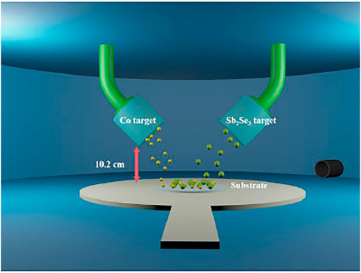
FIGURE 1. The process of preparing Co-doped Sb2Se3 by using magnetron sputtering technology.
Instruments
The morphology and thickness of pure and Co-doped Sb2Se3 nanofilms were obtained by field-scanning electron microscope (SU70, Hitachi, Japan), the X-ray diffraction analysis of pure and Co-doped Sb2Se3 nanofilms was carried out by using an X-ray diffractometer (XRD; D8, Bruker, Germany). The elemental analysis of Co-doped Sb2Se3 nanofilms was tested by energy dispersive spectroscopy (EDS; XM260S, AmetekGenesis, United States). The transmittance and linear absorption spectra of the pure and Co-doped Sb2Se3 nanofilms were characterized by the spectrophotometer (Uv-Vis; Uv-3600i PLUS, SHIMADZU, Japan).
In the transient absorption experiment, by changing the optical path difference between the detecting and pumping light, a variation of the white supercontinuum spectrum with different delay times can be obtained. Thus, the frequency-doubled Yb:KGW laser was selected for the transient absorption experiment, and the laser can provide 190 femtosecond (fs) laser pulses at 450 nm. In the fs transient absorption experiment, the repetition rate, probe pulses, and specific pump fluence were set at 137 Hz, 800–1,050 nm, and 82 μJ/ cm2, respectively (Fang et al., 2015; Fang et al., 2016). The nonlinear optical characteristics of the pure and Co-doped Sb2Se3 nanofilms were tested by fs Z-Scan experiments. The light source used an optical parameter amplifier (OPA, Light Conversion ORPHEUS), which was pumped by a mode-locked Yb:KGW fiber laser. The measurement parameters were set at 190 fs pulse and 20 Hz, and the waist radius of the laser was 33 µm. The energies of the laser excitation were set at 300, 400, and 500 nJ, respectively.
Results and Discussion
Structural and Compositional Analysis
Figure 2 shows the XRD patterns of the Sb2Se3 and the Co-doped Sb2Se3 nanofilms. It can be seen from the XRD patterns that Co-doped Sb2Se3 nanofilms were successfully prepared and exhibited a polycrystalline structure. According to the XRD pattern, compared with the Sb2Se3 nanofilm (PDF#15-0816) (Zhou et al., 2015; Liu et al., 2019), the diffraction characteristic peak (310) of Co-doped Sb2Se3 nanofilms increased, and the lattice spacing of the (310) is 3.669 nm. In addition, the diffraction characteristic peaks of the Co-doped Sb2Se3 films exhibit an increasing trend with the increase of Co dopant. It can be clearly seen from the XRD patterns that the diffraction characteristic peaks of the Co-doped Sb2Se3 nanofilms are located at 24.575 (0.5 W), 24.441 (1.0 W), and 24.296 (1.5 W), respectively, which are all offset compared with the diffraction characteristic peaks of the pure Sb2Se3 nanofilm (24.987). In addition, the lattice constants of the Co-doped Sb2Se3 nanofilms are also calculated as 11.839 (0.5 W), 11.853 (1 W), and 11.891 (1.5 W), respectively, which are all smaller than the lattice constant of pure Sb2Se3 (11.902). In past reports, Co dopants in the Sb2Se3 system can be used as a substitute site of Sb or Se as well as interstitial atoms (Li et al., 2016; Mahani and El-Sayad, 2019). Under the premise that Se and Sb are abundant enough, Co can effectively replace Sb to form the most favorable structure. If the Sb position in Sb2Se3 is successfully replaced by some dopant, the homologous diffraction characteristic peaks are shifted and exhibited in the XRD pattern. The shift of the characteristic diffraction peaks was observed in the Co-doped Sb2Se3 nanofilms, confirming that the Co doping is at the grain boundary of Sb2Se3 rather than entering its lattice and that the Co dopant may also enter the substitution site of Sb. The supercell of Co-doped Sb2Se3 was shown in Figure 3.
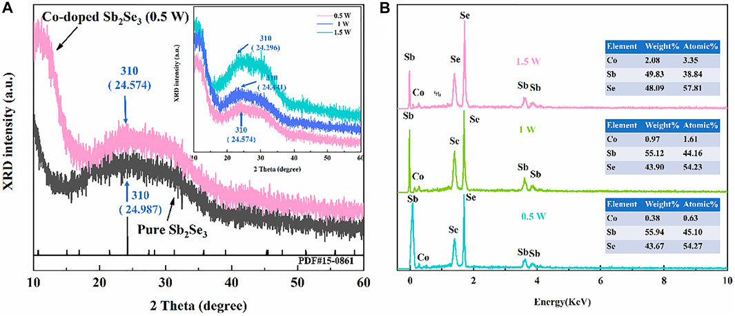
FIGURE 2. (A) The XRD patterns of Co-doped and pure Sb2Se3 nanofilms. (B) The EDS of Co-doped Sb2Se3.
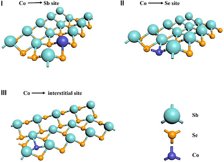
FIGURE 3. The structures of Sb2Se3 with Co on (I) Sb (II) Se, and (III) interstitial site.
The elemental composition of the Co-doped Sb2Se3 nanofilms was detected by EDS. The results of the EDS show that, with the increase of DC sputtering power in the Co target, the Co content of the Co-doped Sb2Se3 nanofilms increases, but the peak positions of the Se and Sb in the film have not shifted, and the content of Co in the Co-doped Sb2Se3 nanofilms was 0.63% (0.5 W), 1.61% (1.0 W), and 3.35% (1.5 W), respectively. The results of the EDS provide strong evidence for Co successfully doping at grain boundaries of Sb2Se3. Although the Co doping amount increases, the resistance of the Sb2Se3 grain boundary gradually decreases, which leads to the formation of a space charge region near the grain boundary.
Morphological and Optical Analysis
To study the morphology and thickness of pure and Co-doped Sb2Se3 nanofilms, the nanofilms were characterized by SEM, and the results are shown in Figure 4. The nanofilms that were prepared by magnetron sputtering are smooth uniform and free of cracks. In addition, we also characterize the thickness of the pure and Co-doped Sb2Se3 nanofilms. The thicknesses of the pure and Co-doped Sb2Se3 nanofilms are both 150 nm. According to previous reports (Cattaruzza et al., 2009; Wu et al., 2015; Hymavathi et al., 2017), the morphology of doped films is determined by the deposition conditions, particularly the power of direct current magnetron sputtering. In accordance with the result of the elemental mapping (Figure 4(f ∼ h)), the elements of Sb, Se, and Co are uniformly dispersed in the entire Co-doped Sb2Se3 nanofilms.
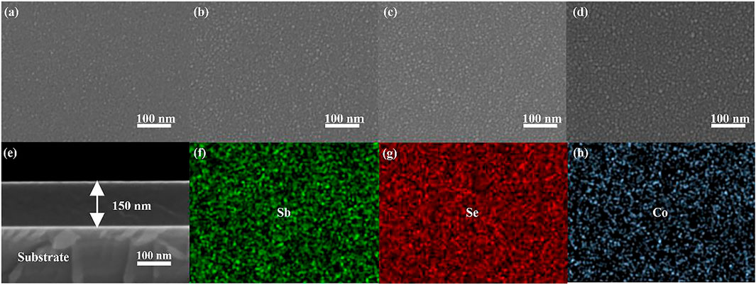
FIGURE 4. (A–D) The SEM of pure and Co-doped Sb2Se3 nanofilms. (E) The thickness of pure and Co-doped Sb2Se3 nanofilms. (F–H) The elemental mapping of Co-doped Sb2Se3 (1.5 W) nanofilms.
Figure 5 shows that the transmittance and absorption spectrum of pure and Co-doped Sb2Se3 nanofilms were obtained by spectrophotometer. The linear absorption edge of the optical bandwidths of the pure and Co-doped Sb2Se3 nanofilms at near infrared can be found. Compared with the pure Sb2Se3 nanofilms, the red shift of the linear absorption edge of the Co-doped Sb2Se3 nanofilms can be attributed to the different ionic radius of Co than that of Sb, which changes the bond length with Se at replacement Sb, thus leading to a change in the eigenfrequency. The change of the eigenfrequency moves the linear absorption edge of the Co-doped Sb2Se3 nanofilms and, hence, the red shift (Tian and Liu, 2006). Furthermore, the increase in Co dopant content leads to increasing the deficiency, which leads to an increase in the average atomic distance, thus leading to a decrease in the energy level spacing. For linear absorption, we have Tacu’s formulation, which is given as follows (Filipchenko and Naurizbaev, 1976):
where the coefficient of linear absorption is denoted by α, A represents a constant, Eg represents the optical band gap, n represents an index (n = 1, 2, 3), and the incident photon energy is denoted by hν. The optical band gap (Eg) values of the pure and Co-doped Sb2Se3 nanofilms (0.5, 1.0, and 1.5 W) are, respectively, calculated as 1.93, 1.83, 1.80, and 1.77 eV. Figures 5C,D exhibit the transmission spectrum of the pure and Co-doped Sb2Se3 nanofilms. It can be clearly seen that the A and B thin films both exhibit more than 80% transmission in the range of 800–1,100 nm, and the dopant of Co has no effect on the transmittance at near infrared.
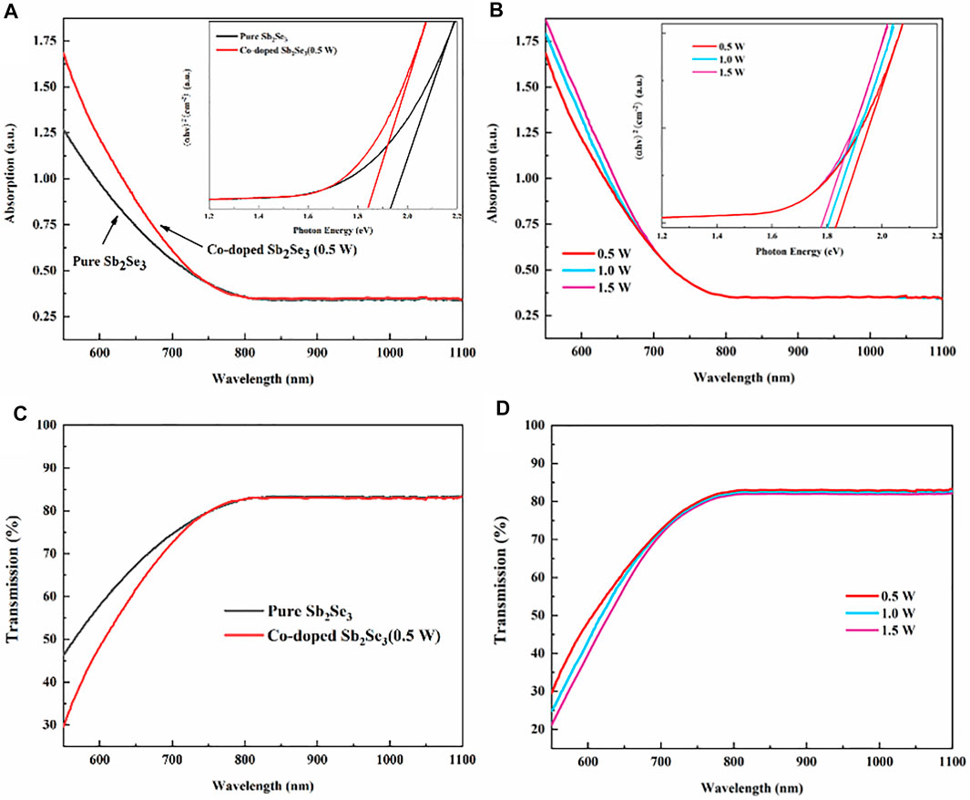
FIGURE 5. (A, B) The linear absorption spectrum of pure and Co-doped Sb2Se3 nanofilms. The inset shows the relationship between the incident photon energy and absorbance. (C) and (D) exhibit the transmittance spectrum of pure and Co-doped Sb2Se3 nanofilms.
Nonlinear Optical Properties
The nonlinear signals of the pure and Co-doped Sb2Se3 nanofilms, which were obtained by fs Z-scan experiment at 800, 980, and 1,030 nm, are used to understand the mechanism of the nonlinear response and regulation. The open-aperture (OA) Z-scan results of the pure and Co-doped Sb2Se3 nanofilms are shown in Figure 6(a∼c). For the pure and Co-doped Sb2Se3 nanofilms, the RSA phenomenon was observed at 800 nm, and no signals were obtained at 980 and 1,030 nm for the pure Sb2Se3 nanofilm. Through the linear absorption spectroscopy of the pure and Co-doped Sb2Se3 nanofilms, it can be seen that the Eg of the pure and Co-doped Sb2Se3 nanofilms are greater than hv but less than 2hv, which indicates that the pure and Co-doped Sb2Se3 nanofilms both exhibit a TPA. For the Co-doped Sb2Se3 nanofilms, the OA Z-scan signals were exhibited at 980 and 1,030 nm, and it also shows that, with the increase of the doping concentration, the amplitude of the OA Z-scan signals exhibited the corresponding increase. In addition, we also obtained the OA Z-scan signals of the pure and Co-doped Sb2Se3 nanofilms (1.5 W) under different excitation energy at 800 nm. For the pure Sb2Se3 nanofilm, with the increase of the excitation energy, the OA Z-scan signals did not change; therefore, it can be inferred that the pure Sb2Se3 is a pure third-order nonlinear effect, and the OA Z-scan signal amplitude of the Co-doped Sb2Se3 nanofilms (1.5 W) increased with the increase of the excitation energy. Therefore, we infer that the Co-doped Sb2Se3 nanofilms have a higher-order nonlinear absorption phenomenon, that is, FCA. For the higher-order nonlinear absorption phenomenon, we have (Lakhwani et al., 2010)
Here, α represents the global absorption coefficient, γ stands for the fifth-order nonlinear absorption coefficient, T(z) stands for the normalized transmittance, β represents the third nonlinear absorption coefficient of the thin films, and I0 stands for the light intensity at the focus. The effective thickness of the nanofilms is denoted by Leff, and
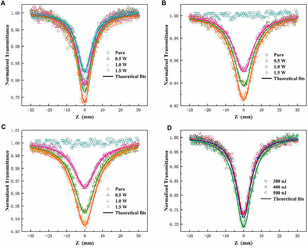
FIGURE 6. The OA Z-scan signals of pure and Co-doped Sb2Se3 nanofilms at 800 (A), 980, (B), and 1,030 nm (C). The OA Z-scan signal of Co-doped Sb2Se3 nanofilm (1.5 W) thin films at 800 nm under different excitation conditions (D).
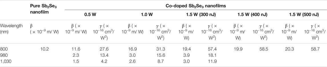
TABLE 1. Nonlinear absorption parameters of the Co-doped and pure Sb2Se3 nanofilms under different excitation conditions.
The calculated results show that, with the increase of excitation energy, the values of β and γ of the Co-doped Sb2Se3 nanofilms increase correspondingly, thus confirming that there is FCA in the Co-doped Sb2Se3 nanofilms. As is known to all, the interaction between matter and light can be effectively increased by Co nanoparticles, which can also illustrate the high carrier mobility (Han et al., 2006; Ahlam et al., 2012). In addition, Co nanoparticles can effectively capture photogenerated carriers and can also inhibit the combination of carriers and holes in the local electric field (Li et al., 2017; Nasir et al., 2017). The formation of the space charge region formed by the Co dopant leads to a larger electron base, so the probability of transition becomes larger during the absorption of photon energy and the increase of the Co dopant content can provide more free carriers; thus, the increment of the free carriers leads to the enhancement of the nonlinear effect. Owing to the increase of excited state absorption and high carrier mobility brought by Co nanoparticles, FCA and TPA are successfully set up in the Co-doped Sb2Se3 nanofilms with the successful doping of Co into Sb2Se3. Therefore, the RSA behavior of the Co-doped Sb2Se3 nanofilms was observed at 980 and 1,030 nm. As the content of the Co dopant increases, the intensity of RSA behavior exhibits a corresponding increase. This phenomenon is because the increase of the content of Co dopant can provide more Co nanoparticles, thus providing more free carriers, which can further promote faster and stronger absorption in the excited state.
The CA Z-scan signals (800, 980, and 1,030 nm) of the pure and Co-doped Sb2Se3 nanofilms were obtained by using the CA fs Z-scan experiment as shown in Figure 7. For the pure Sb2Se3 nanofilm, the CA Z-scan signal was observed at 800 nm, which can be attributed to Kerr refraction caused by the nonlinear systematic dispersion of bound electrons appearing near the intrinsic absorption edge although there was no CA Z-scan signal observed at 980 and 1,030 nm, and it can be caused by the weak Kerr refraction. For the Co-doped Sb2Se3 nanofilms, the CA Z-scan signals were observed at 800, 980, and 1,030 nm, which indicates the existence of high-order nonlinear refraction (FCR). In addition, with the increase of the Co dopant content, the amplitude of the CA Z-scan signals increased correspondingly. According to the results of the OA Z-scan signals of the Co-doped Sb2Se3 nanofilms, with the increase of the Co dopant content, more Co nanoparticles can be provided, which led to the increase of photogenerated carriers. Therefore, it can be concluded that the content of photogenerated carriers in the Co-doped Sb2Se3 nanofilms is relatively high, and the excess carriers can participate in the refraction of free carriers. Thus, it can be concluded that there are FCR at 980 and 1,030 nm, and the FCR is dominant. According to the plasma dispersion effect of carriers, the refraction effect of free carriers increases with the increase of incident wavelength (Soref and Bennett, 1987; Gao et al., 2005). Therefore, the Co-doped Sb2Se3 nanofilms exhibit a self-defocusing behavior at 980 and 1,030 nm, which are constructed by the FCR and Kerr refraction. In addition, we also obtained the CA Z-scan signals of the Co-doped Sb2Se3 nanofilm (1.5 W) and pure Sb2Se3 nanofilm, which were excited under different excitation energy at 800 nm as shown in Figure 7D. For the pure Sb2Se3 nanofilm, there was no change in CA Z-scan signals. For the Co-doped Sb2Se3 nanofilm (1.5 W), the signals of the CA Z-scan indicate that the amplitude of the nonlinear signal increases with the increase of the excitation energy. The reason for the phenomenon is that, with the increase of the excitation energy, excess carriers, which can participate in the refraction of the free carriers, are generated, thus leading to the enhancement of the refraction of the free carriers (Fang et al., 2013).
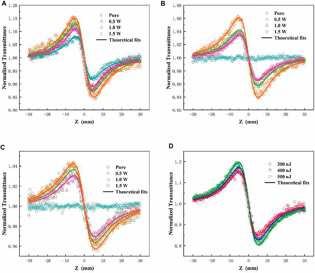
FIGURE 7. The CA Z-scan signals of the Co-doped Sb2Se3 nanofilms at 800 (A), 980 (B), and 1,030 nm (C). (D) The CA Z-scan signals of Co-doped Sb2Se3 nanofilms (1.5 W) at 800 nm under different excitation conditions (300, 400, and 500 nJ).
For nonlinear refraction, we assume that the incident laser has a Gaussian distribution, and then the sample transmittance on the far-field axis is proportional to the phase shift (Gao et al., 2005).
The effective thickness of the samples is denoted by Leff, and
The values of n2 can be calculated by using Eqs 4–6 and are shown in Table 2.
TABLE 2. Nonlinear refractive index of pure and Co-doped Sb2Se3 nanofilms under different excitation conditions.
Transient Absorption Analysis
The nonlinear optical properties of pure and Co-doped Sb2Se3 nanofilms were studied by transient absorption experiment. To ensure the excitation efficiency, the pumping light was set at 450 nm. The change of absorption intensity at a specific wavelength can be represented as the variation of the optical density (ΔOD), which is obtained by transient absorption spectroscopy. For the transient absorption experiment, ΔOD can be calculated as (Li et al., 2014)
where λp represents the wavelength of probing light, Ton represents the light of the probe, t stands for the delay time and the total transmittance of pumping, and the transmittance of probing light is denoted by Toff.
For the pure Sb2Se3 nanofilms, the RSA phenomenon was observed at 780–830 nm (ΔOD>0), but no nonlinear signal was detected in other probe regions (Figures 8A,B), which is in synchrony with the result of the fs Z-scan signal of the pure Sb2Se3 nanofilms. According to the results of linear absorption of the pure Sb2Se3 nanofilm, TPA occurs when the optical bandgap (Eg) is greater than hν and less than 2hν. With the successful doping of Co into Sb2Se3, TPA and FCA are successfully established in the Co-doped Sb2Se3 nanofilms, which is due to the increase of carrier mobility and excited-state absorption brought by Co nanoparticles. Co-doped Sb2Se3 nanofilms exhibit the RSA phenomenon with high transient absorption (ΔOD > 6.5), broadband nonlinear response (800–1,030 nm), and ultrafast carrier absorption (<1 picoseconds) at near infrared at Figures 8C,D compared with Sb2Se3 nanofilms.
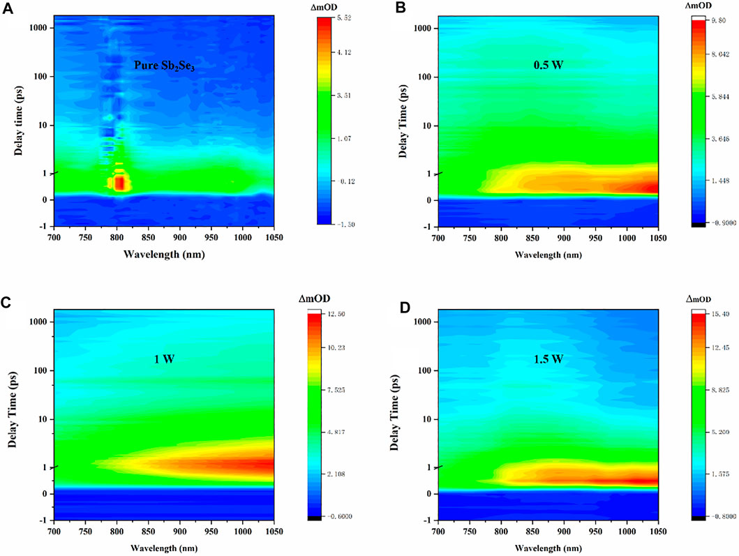
FIGURE 8. (A) The results of the transient absorption experiment of the pure Sb2Se3 nanofilm at near infrared. (C–D) The results of the transient absorption experiment of Co-doped Sb2Se3 (0.5, 1, and 1.5 W) nanofilms at near infrared.
Although the content of Co dopant increases, the carrier absorption rate and intensity of RSA of the Co-doped Sb2Se3 nanofilms exhibit a corresponding increase. In addition, the increase in the doping amount of Co can provide more Co nanoparticles, which can further promote the absorption of the excited state faster and stronger. When the DC sputtering power was increased to 1.5 W, the Co-doped Sb2Se3 nanofilm exhibited the strongest transient absorption (ΔOD > 15) and ultrafast carrier absorption (<1 picoseconds) as shown in Figure 8D. Through the analysis of the transient spectrum, it can be seen that the transient absorption intensity of all Co-doped Sb2Se3 nanofilm is 800 < 980 < 1,030 nm; according to the plasma dispersion effect of carriers, the absorption and refraction effects of free carriers increase with the increase of incident wavelength. It is further confirmed that FCA and FCR play a dominant role in the nonlinear response at 980 and 1,030 nm. In all the transient absorption spectra, it can be found that the signal has no obvious movement during the whole delay time, which suggests that the TPA and FCA may be from the uniform energy level during the whole delay time (He et al., 2010). In addition, the sapphire substrate has no influence on the transient absorption experiment of the Co-doped and pure Sb2Se3 nanofilms. Moreover, the differences between Co-doped and pure Sb2Se3 nanofilms were measured by the Gaussian beam focal plane, which proves that the Co-doped and pure Sb2Se3 nanofilms do not suffer optical damage in the transient absorption experiment. Figure 10 exhibits the schematic diagram of the energy levels of the Co-doped and pure Sb2Se3 nanofilms, one-photon absorption, and FCR.
Figure 9 shows the transient absorption fitting curves of pure and Co-doped Sb2Se3 (0.5, 1, and 1.5 W) nanofilms at different time scales under 450 nm laser excitation. For the pure and Co-doped Sb2Se3 nanofilms, there was no influence between the pump light and the carrier relaxation, which proves that the transient absorption experiment was carried out under steady conditions. Multiple exponential functions are selected to fit the transient absorption curve of the pure and Co-doped Sb2Se3 nanofilms, and the formula is as follows (Fang et al., 2017):
where C3, C2, and C1 represent the amplitudes of the third, second, and first components, respectively. For the pure Sb2Se3 nanofilm, which was excited by 450 nm, the carrier relaxation time values (τ1 and τ2) were calculated as 1.74 ± 0.74 ps and 3.89 ± 0.73 ns. The values of transient absorption (τ1, τ2, and τ3) of the Co-doped Sb2Se3 nanofilms under the same laser excitation were calculated as 1.58 ± 0.9 ps, 12.39 ± 0.21 ps, and 4.42 ± 0.82 ns (0.5 W); 1.32 ± 0.49 ps, 13.35 ± 0.4 ps, and 4.63 ± 0.81 ns (1.0 W); and 1.73 ± 0.99 ps, 12.03 ± 0.26 ps, and 4.89 ± 0.79 ns (1.5 W), respectively. The calculated results show that the doping amount of Co can adjust the carrier relaxation time of the Sb2Se3 nanofilms. In addition, the results also confirm that Co nanoparticles can effectively inhibit the composite process of carrier and hole, thus improving the FCA efficiency. The carrier relaxation processes for the pure and Co-doped Sb2Se3 nanofilms are shown in Figure 10. In the whole relaxation process of pure and Co-doped Sb2Se3 nanofilms, the different relaxation mechanisms determine the relaxation time of carriers at different steps. For the pure Sb2Se3 nanofilms, the τ1 is caused by the cooling of thermal carriers, and the τ2 is caused by the relaxation of nonradiative transition of carriers in the optical bandgap. Although for the Co-doped Sb2Se3 nanofilms, τ3 is caused by the relaxation of nonradiative transition of carriers from CB to VB, the τ2 is caused by the relaxation of nonradiative transition of carriers from CB to doping level, and the τ1 is caused by the electron-phonon scattering.
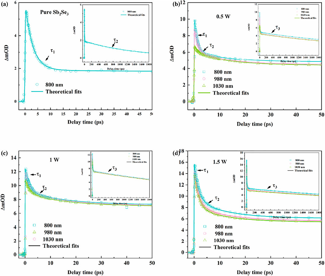
FIGURE 9. (A) The transient nonlinear curve of pure Sb2Se3 nanofilm at different time scales. (B–D) The transient nonlinear curve of Co-doped Sb2Se3 (0.5, 1.0, and 1.5 W) thin films at different time scales.
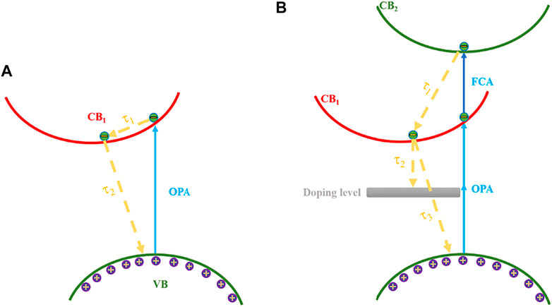
FIGURE 10. (A) The process of pure Sb2Se3 nanofilm carrier relaxation time, OPA, and band. (B) The illustration of Co-doped Sb2Se3 nanofilm carrier relaxation time, OPA, and band.
Conclusion
In conclusion, this study confirms that the enhancement of excited state absorption at near infrared caused by FCA, FCR, TPA, and Kerr refraction is the main mechanism of the broadband nonlinear response of Co-doped Sb2Se3 films, which were prepared by magnetron sputtering. Compared with the pure Sb2Se3 nanofilm, the Co-doped Sb2Se3 nanofilms exhibit the following superior nonlinear optical properties. (I) Co-doped Sb2Se3 nanofilms exhibit ultrafast carrier absorption (ps) at near infrared and excellent broadband nonlinear response (800–1,030 nm). (II) High nonlinear absorption coefficients, high nonlinear refraction index, long carrier relaxation time, and the ultrafast carrier absorption of Co-doped Sb2Se3 nanofilms are determined by the content of the Co dopant. (III) The transient absorption intensity of Co-doped Sb2Se3 nanofilms (1.5 W) is achieved ΔOD>15. Finally, the Co-doped Sb2Se3 nanofilms provide more reference value for selecting more suitable elements as the dopants of Sb2Se3 to prepare the broadband nonlinear optical devices.
Data Availability Statement
The original contributions presented in the study are included in the article/supplementary material, further inquiries can be directed to the corresponding author.
Author Contributions
DS contributed to conception and design of the study. WHS organized the database. DS wrote the first draft of the manuscript. YF, WUS, QM, and XY contributed to manuscript revision, read, and approved the submitted version.
Funding
This work is supported by the National Natural Science Foundation of China (Grant No. 11504072), Natural Science Foundation of Heilongjiang Province (Grant No. LH 2020F032) and (Grant LH 2019A018); Key Laboratory for Photonic and Electronic Bandgap Material (Ministry of Education) and School of Physics and Electronic Engineering of Harbin Normal University of China, National Natural Science Foundation of China (No. 11704273), and Natural Science Foundation of Jiangsu Province, China (Grant No. BK20170375).
Conflict of Interest
The authors declare that the research was conducted in the absence of any commercial or financial relationships that could be construed as a potential conflict of interest.
Publisher’s Note
All claims expressed in this article are solely those of the authors and do not necessarily represent those of their affiliated organizations, or those of the publisher, the editors and the reviewers. Any product that may be evaluated in this article, or claim that may be made by its manufacturer, is not guaranteed or endorsed by the publisher.
References
Ahlam, M. A., Ravishankar, M. N., Vijayan, N., Govindaraj, G., Upadhyaya, V., and Prakash, A. P. G. (2012). The Effect of Co-60 Gamma Irradiation on Optical Properties of Some Nonlinear Optical (NLO) Single Crystals. J. Opt. 41, 158–166. doi:10.1007/s12596-012-0079-8
Ai, Y., Hsu, T. H., Wu, D. C., Lee, L., Chen, J.-H., Chen, Y.-Z., et al. (2018). An Ultrasensitive Flexible Pressure Sensor for Multimodal Wearable Electronic Skins Based on Large-Scale Polystyrene ball@reduced Graphene-Oxide Core-Shell Nanoparticles. J. Mater. Chem. C 6, 5514–5520. doi:10.1039/C8TC01153B
Andreev, Y. M., Kokh, K. A., Lanskii, G. V., and Morozov, A. N. (2011). Structural Characterization of Pure and Doped GaSe by Nonlinear Optical Method. J. Cryst. Growth 318, 1164–1166. doi:10.1016/j.jcrysgro.2010.10.194
Cao, X. Y., Xin, J. B., Wang, Y. Y., Hu, J. M., and Qu, X. R. (2014). Preparation of Er-Doped (Bi2Te3)0.90(Sb2Te3)0.05(Sb2Se3)0.05 by Mechanical Alloying and its Thermoelectric Properties. Mater. Sci. Eng. B Solid State. Mater. Adv. Technol. 188, 54–58. doi:10.1016/j.mseb.2014.06.007
Cattaruzza, E., Battaglin, G., Visentin, F., and Trave, E. (2009). Er-doped SiO2 Films by Rf Magnetron Co-sputtering. J. Non-Crystalline Sol. 355, 1128–1131. doi:10.1016/j.jnoncrysol.2008.11.031
Choi, J., Lee, H.-W., Kim, B.-S., Park, H., Choi, S., Hong, S. C., et al. (2006). Magnetic and Transport Properties of Mn-Doped Bi2Se3 and Sb2Se3. J. Magnetism Magn. Mater. 304, e164–e166. doi:10.1016/j.jmmm.2006.02.041
Djordjevic, I. B., and Arabaci, M. (2010). LDPC-coded Orbital Angular Momentum (OAM) Modulation for Free-Space Optical Communication. Opt. Express 18, 24722–24728. doi:10.1364/OE.18.024722
Fang, Y., Wu, X.-Z., Ye, F., Chu, X.-Y., Li, Z.-G., Yang, J.-Y., et al. (2013). Dynamics of Optical Nonlinearities in GaN. J. Appl. Phys. 114, 103507. doi:10.1063/1.4820929
Fang, Y., Xiao, Z., Wu, X., Zhou, F., Yang, J., Yang, Y., et al. (2015). Optical Nonlinearities and Ultrafast All-Optical Switching of M-Plane GaN in the Near-Infrared. Appl. Phys. Lett. 106, 251903. doi:10.1063/1.4923184
Fang, Y., Yang, J., Xiao, Z., Zhang, J., Chen, Y., Wu, Q., et al. (2017). Ultrafast All-Optical Modulation in Fe-Doped GaN at 1.31 and 1.55 μm with High Contrast and Ultralow Power. Appl. Phys. Lett. 110, 161902. doi:10.1063/1.4980090
Fang, Y., Yang, J., Yang, Y., Wu, X., Xiao, Z., Zhou, F., et al. (2016). Ultrafast Carrier Dynamics in Ap-type GaN Wafer under Different Carrier Distributions. J. Phys. D: Appl. Phys. 49, 045105. doi:10.1088/0022-3727/49/4/045105
Filipchenko, A. S., and Naurizbaev, A. (1976). Moss-burstein Effect in N-type Crystals of Indium Antimonide. Phys. Stat. Sol. (A) 37, K139–K142. doi:10.1002/pssa.2210370252
Gao, Y., Zhang, X., Li, Y., Liu, H., Wang, Y., Chang, Q., et al. (2005). Saturable Absorption and Reverse Saturable Absorption in Platinum Nanoparticles. Opt. Commun. 251, 429–433. doi:10.1016/j.optcom.2005.03.003
Han, H., Song, Y., Hou, H., Fan, Y., and Zhu, Y. (2006). A Series of Metal-Organic Polymers Assembled from MCl2(M = Zn, Cd, Co, Cu): Structures, Third-Order Nonlinear Optical and Fluorescent Properties. Dalton Trans. 16, 1972–1980. doi:10.1039/b514431k
He, X., Wang, Y., Yang, Z., Ma, Y., and Yang, Y. (2010). Cooperative Enhancement of TPA in Cruciform Double-Chain DSB Derivation: a Femtosecond Transient Absorption Spectra Study. Appl. Phys. B 100, 773–777. doi:10.1007/s00340-010-4161-0
Henari, F. Z., and Dakhel, A. A. (2011). Observation of Simultaneous Reverse Saturation Absorption and Saturation Absorption in Silver Nanoparticles Incorporated into Europium Oxide Thin Film. Opt. Commun. 284, 651–655. doi:10.1016/j.optcom.2010.09.090
Hymavathi, B., Rajesh Kumar, B., and Subba Rao, T. (2017). Thickness Dependent Optical Dispersion Parameters and Nonlinear Optical Properties of Nanostructured Cr Doped CdO Thin Films. Opt. Quant Electron. 49, 86. doi:10.1007/s11082-017-0935-5
Jia, J., Wu, X., Fang, Y., Yang, J., Guo, X., Xu, Q., et al. (2018). Ultrafast Broad-Band Optical Limiting in Simple Hydrazone Derivatives with a Π-Conjugated System: Effect of Two-Photon-Induced Singlet-State Absorption. J. Phys. Chem. C 122, 16234–16241. doi:10.1021/acs.jpcc.8b02149
Jiang, J., Hu, W., Xie, D., Yang, J., He, J., Gao, Y., et al. (2019). 2D Electric-Double-Layer Phototransistor for Photoelectronic and Spatiotemporal Hybrid Neuromorphic Integration. Nanoscale 11, 1360–1369. doi:10.1039/C8NR07133K
Lakhwani, G., Roijmans, R. F. H., Kronemeijer, A. J., Gilot, J., Janssen, R. A. J., and Meskers, S. C. J. (2010). Probing Charge Carrier Density in a Layer of Photodoped ZnO Nanoparticles by Spectroscopic Ellipsometry. J. Phys. Chem. C 114, 14804–14810. doi:10.1021/jp104846h
Lee, H., Yang, W., Tan, J., Oh, Y., Park, J., and Moon, J. (2019). Cu-Doped NiOx as an Effective Hole-Selective Layer for a High-Performance Sb2Se3 Photocathode for Photoelectrochemical Water Splitting. ACS Energ. Lett. 4, 995–1003. doi:10.1021/acsenergylett.9b00414
Li, H. B., Qiao, Y. F., Li, J., Fang, H. L., Fan, D. H., and Wang, W. (2017). A Sensitive and Label-free Photoelectrochemical Aptasensor Using Co-doped ZnO Diluted Magnetic Semiconductor Nanoparticles. Biosens. Bioelectron. 94, 554–565. doi:10.1016/j.bios.2015.09.066
Li, Y., Zhou, Y., Zhu, Y., Chen, C., Luo, J., Ma, J., et al. (2016). Characterization of Mg and Fe Doped Sb2Se3 Thin Films for Photovoltaic Application. Appl. Phys. Lett. 109, 232104. doi:10.1063/1.4971388
Li, Z.-g., Zhao, R., Li, W., Wang, H., Yang, H., and Song, Y.-l. (2014). Strain Dependent Ultrafast Carrier Dynamics in EuTiO3 Films. Appl. Phys. Lett. 105, 162904. doi:10.1063/1.489878710.1063/1.4898787
Lin, H., Chen, L., Zhou, L.-J., and Wu, L.-M. (2013). Functionalization Based on the Substitutional Flexibility: Strong Middle IR Nonlinear Optical Selenides AXII4XIII5Se12. J. Am. Chem. Soc. 135, 12914–12921. doi:10.1021/ja4074084
Liu, C., Yuan, Y., Cheng, L., Su, J., Zhang, X., Li, X., et al. (2019). Tunable Nonlinear Optical Absorption in Amorphous and Crystalline Sb2Se3 Thin Films. J. Alloys Comp. 791, 753–760. doi:10.1016/j.jallcom.2019.03.295
Mahani, R., and El-Sayad, E. A. (2019). Effect of Sulfur Doping on the Dielectric Properties of Sb2Se3 System. J. Adv. Dielect. 09, 1950001. doi:10.1142/S2010135X19500012
Major, A., Yoshino, F., Aitchison, J. S., Smith, P. W. E., Sorokin, E., and Sorokina, I. T. (2004). Ultrafast Nonresonant Third-Order Optical Nonlinearities in ZnSe for Photonic Switching at Telecom Wavelengths. Appl. Phys. Lett. 85, 4606–4608. doi:10.1063/1.1823599
Medina, H., Li, J.-G., Su, T.-Y., Lan, Y.-W., Lee, S.-H., Chen, C.-W., et al. (2017). Wafer-Scale Growth of WSe2 Monolayers toward Phase-Engineered Hybrid WOx/WSe2 Films with Sub-ppb NOx Gas Sensing by a Low-Temperature Plasma-Assisted Selenization Process. Chem. Mater. 29, 1587–1598. doi:10.1021/acs.chemmater.6b04467
Molli, M., Pradhan, P., Dutta, D., Jayaraman, A., Bhat Kademane, A., Muthukumar, V. S., et al. (2016). Study of Nonlinear Optical Absorption Properties of Sb2Se3 Nanoparticles in the Nanosecond and Femtosecond Excitation Regime. Appl. Phys. A. 122, 549. doi:10.1007/s00339-015-9568-3
Nasir, Z., Shakir, M., Wahab, R., Shoeb, M., Alam, P., Khan, R. H., et al. (2017). Co-precipitation Synthesis and Characterization of Co Doped SnO 2 NPs, HSA Interaction via Various Spectroscopic Techniques and Their Antimicrobial and Photocatalytic Activities. Int. J. Biol. Macromolecules 94, 554–565. doi:10.1016/j.ijbiomac.2016.10.057
Ning, H., Guo, H., Zhang, J., Wang, X., Jia, X., Qiu, J., et al. (2021). Enhancing the Efficiency of Sb2S3 Solar Cells Using Dual-Functional Potassium Doping. Solar Energ. Mater. Solar Cell 221, 110816. doi:10.1016/j.solmat.2020.110816
Radisavljevic, B., and Kis, A. (2013). Mobility Engineering and a Metal-Insulator Transition in Monolayer MoS2. Nat. Mater 12, 815–820. doi:10.1038/NMAT3687
Ren, D., Luo, X., Chen, S., Zheng, Z., Cathelinaud, M., Liang, G., et al. (2020). Structure, Morphology, and Photoelectric Performances of Te-Sb2Se3 Thin Film Prepared via Magnetron Sputtering. Nanomaterials 10, 1358–1371. doi:10.3390/nano10071358
Soref, R., and Bennett, B. (1987). Electrooptical Effects in Silicon. IEEE J. Quan. Electron. 23, 123–129. doi:10.1109/JQE.1987.1073206
Tian, F. H., and Liu, C. B. (2006). DFT Description on Electronic Structure and Optical Absorption Properties of Anionic S-Doped Anatase TiO2. J. Phys. Chem. B 110, 17866–17871. doi:10.1021/jp0635462
Tuhl, A., Manaa, H., Makhseed, S., Al-Awadi, N., Mathew, J., Ibrahim, H. M., et al. (2012). Reverse Saturation Absorption Spectra and Optical Limiting Properties of Chlorinated Tetrasubstituted Phthalocyanines Containing Different Metals. Opt. Mater. 34, 1869–1877. doi:10.1016/j.optmat.2012.05.018
Volz, T., Reinhard, A., Winger, M., Badolato, A., Hennessy, K. J., Hu, E. L., et al. (2012). Ultrafast All-Optical Switching by Single Photons. Nat. Photon 6, 605–609. doi:10.1038/nphoton.2012.181
Wang, J., Yang, C., Huang, Z., Humphrey, M. G., Jia, D., You, T., et al. (2012). Seed-catalyzed Heteroepitaxial Growth and Nonlinear Optical Properties of Zinc Selenide Nanowires. J. Mater. Chem. 22, 10009–10014. doi:10.1039/c2jm00091a
Wu, M., Yu, S., Chen, G., He, L., Yang, L., and Zhang, W. (2015). Structural, Optical, and Electrical Properties of Mo-Doped ZnO Thin Films Prepared by Magnetron Sputtering. Appl. Surf. Sci. 324, 791–796. doi:10.1016/j.apsusc.2014.11.039
Keywords: Co-doped Sb2Se3 nanofilms, ultrafast broadband response, near-infrared, ultrafast carrier absorption, reverse saturation absorption
Citation: Sun D, Fang Y, Yan X, Shan W, Sun W and Meng Q (2021) Ultrafast Broadband Nonlinear Optical Response in Co-Doped Sb2Se3 Nanofilms at Near-Infrared. Front. Mater. 8:721101. doi: 10.3389/fmats.2021.721101
Received: 06 June 2021; Accepted: 09 August 2021;
Published: 13 September 2021.
Edited by:
Zhongquan Nie, Taiyuan University of Technology, ChinaReviewed by:
Zhongguo Li, Changshu Institute of Technology, ChinaJunyi Yang, Soochow University, China
Copyright © 2021 Sun, Fang, Yan, Shan, Sun and Meng. This is an open-access article distributed under the terms of the Creative Commons Attribution License (CC BY). The use, distribution or reproduction in other forums is permitted, provided the original author(s) and the copyright owner(s) are credited and that the original publication in this journal is cited, in accordance with accepted academic practice. No use, distribution or reproduction is permitted which does not comply with these terms.
*Correspondence: Wenjun Sun, swjgood0139@139.com