Post deposition annealing effect on properties of CdS films and its impact on CdS/Sb2Se3 solar cells performance
 Sajeesh Vadakkedath Gopi1*
  Nicolae Spalatu1*
  Madhawa Basnayaka1
  Robert Krautmann1
  Atanas Katerski1
  Raavo Josepson2 Raitis Grzibovskis3
  Aivars Vembris3 Malle Krunks2
  Ilona Oja Acik1
- 1Department of Materials and Environmental Technology, Tallinn University of Technology, Tallinn, Estonia
- 2Division of Physics, Tallinn University of Technology, Tallinn, Estonia
- 3Institute of Solid State Physics, University of Latvia, Riga, Latvia
Antimony selenide (Sb2Se3) is one of the emerging photovoltaic absorber materials possessing abundance and non-toxicity as the main attributes. Following CdTe technology, CdS is a widely used partner layer for Sb2Se3 solar cells. Related to CdS/Sb2Se3 device configuration, a number of studies reported findings and challenges regarding the intermixing phenomenon at the main interface and suitability of various annealing for CdS (and related interface) and still, significant room remains in developing strategies for interface optimization and understanding of the physiochemistry behind. In this perspective, this work provides a systematic investigation of the effect of vacuum and air annealing at temperatures between 200 and 400°C on the properties of CdS deposited by chemical bath deposition and combined with Sb2Se3 absorber obtained by close-spaced sublimation the direct impact of the CdS annealing on the device performance is illustrated. It is found that by varying the annealing temperature from 200 to 400°C in both, vacuum and air ambient, the morphology of CdS changes from highly dispersed small grain structure to sintered dense grains, the band gap decreases from 2.43 to 2.35 eV and the electron density drops from ∼1018 to ∼1011 cm−3. These changes were correlated with the changes in the CdS lattice and connected with the mobility of the OH group and the presence of secondary phases in CdS layers. 200°C air annealing of CdS was found as an optimal treatment resulting in 2.8% Sb2Se3/CdS cell efficiency - a 60% boost compared to the 1.8% performance of the device with as-deposited CdS. Material and device characterization analysis is performed, providing complementary insights on the interrelation between the physicochemical mechanism of the CdS annealing processes and device functionality.
1 Introduction
Thin film photovoltaic (PV) devices based on antimony selenide (Sb2Se3) absorber materials have attracted intensive research in recent years due to their rapid Photo conversion efficiency (PCE) progress. Besides being composed of Earth-abundant and non-toxic elements, Sb2Se3 has a suitable band gap energy between 1.1–1.3 eV (Li Z. et al., 2019; Tang et al., 2022) and high absorption coefficient of >104 cm−1 in the visible light region (Zhou et al., 2015). These excellent properties make Sb2Se3 a viable addition to copper indium gallium selenide [Cu (In, Ga)Se2] and cadmium telluride (CdTe) solar cells, which have shown PCEs reaching 22% (Green et al., 2021), but for which the scarcity of constituent elements (In, Ga, and Te) is seen as a potential future constraint. The single-phase structure and relatively low melting point at 611°C have enabled the deposition of Sb2Se3 by physical vapor techniques, such as magnetron sputtering (Tang et al., 2019; Chen et al., 2022), close-spaced sublimation (CSS) (Hobson et al., 2020; Spalatu et al., 2021) and vapor transport deposition (VTD) (Wen et al., 2018). To date, almost all the record PCEs for Sb2Se3 PV devices, including the record 9.2% (Li Z. et al., 2019), have been achieved with CSS and VTD fabrication techniques (Krautmann et al., 2023). Since Sb2Se3 is composed of quasi-one-dimensional ribbons, the charge transfer across the absorber film is strongly dependent on which crystal direction the Sb2Se3 ribbons align (Chen et al., 2015). Given that Sb-Se atoms form covalent bonds within ribbons, but adjacent ribbons only bond via weak van der Waals’ forces, vertical (and vertically-tilted) Sb2Se3 ribbons have been deemed optimal for efficient charge transport (Li K. et al., 2019; Hobson et al., 2020; Krautmann et al., 2021). Thus, substantial research efforts have been dedicated to the development of Sb2Se3 absorber films, to deliver suitable processing conditions for optimal grain morphology and orientation [hkl, l = 1] and for efficient Sb2Se3 solar cells (Kumar et al., 2021; Büttner et al., 2022; Campbell et al., 2022; Weiss et al., 2022). Another big focus in the development chain of Sb2Se3-based solar cells has been the identification of a suitable heterojunction partner layer to the Sb2Se3 absorber, where various buffer layers, e.g., cadmium sulfide (CdS) (Weiss et al., 2022), titanium dioxide (TiO2) (Phillips et al., 2019), zinc oxide (ZnO) (Wang et al., 2017), cadmium selenide (CdSe) (Guo et al., 2019), tin oxide (SnO2) (Zhou et al., 2020) have already been tested. Among these, PV devices based on CdS/Sb2Se3 heterojunctions stand out as most prolific, having produced some of the highest PCEs of 8.6% and 7.9% for substrate and superstrate configurations, respectively (Liu et al., 2021; Tang et al., 2022). The choice for CdS, is derived from the fact that this is one of the most established n-type heterojunction (HTJ) partner layers in more mature thin film solar cell technologies such as CIGS (Carron et al., 2019), CdTe (Potlog et al., 2011; 2012) and CZTS (Hernández-Calderón et al., 2020; Punathil et al., 2021). Like in the aforementioned solar cell technologies, CdS (∼2.4 eV) buffer films for Sb2Se3 PV devices are mostly fabricated by a simple and cost-efficient chemical bath deposition (CBD) method. This is particularly the case for state-of-the-art substrate CdS/Sb2Se3 solar cells (Li et al., 2017; Tiwari et al., 2020; Fan et al., 2021; Tang et al., 2022). In CdS/Sb2Se3 PV devices with superstrate configuration, however, various fabrication techniques aside from the CBD method, like magnetron sputtering (Ou et al., 2019; Guo et al., 2020), thermal evaporation (TE) (Kumar et al., 2021) and metal-organic solution coating method (MOSC) (Leng et al., 2021), have been successfully deployed. Another interesting aspect that distinguishes superstrate devices from substrate devices is the common use of post-deposition treatments (PDTs) on the deposited CdS films prior to the Sb2Se3 absorber deposition. Whereas the CdS films in the substrate configuration devices are not often subjected to any PDTs, some groups have tried it and demonstrated it in previous reports (Wen et al., 2018; Ou et al., 2019; Guo et al., 2020; Kumar et al., 2021; Leng et al., 2021; Wang et al., 2022). For instance, superstrate CdS/Sb2Se3 solar cells, with record PCEs of 7.6% (Wen et al., 2018) and 7.9% (Liu et al., 2021), both applied a PDT on CBD-deposited CdS films that involved cadmium chloride (CdCl2) treatment and a following air annealing step at 400°C. Another study demonstrated a PDT on CBD-CdS buffer films involving ammonia etching, which helped achieve a superstrate CdS/Sb2Se3 device with a PCE of 7.5% (Wang et al., 2022). Reports of superstrate CdS/Sb2Se3 solar cells with PCEs of 5.9% (Leng et al., 2021) and 7.4% (Guo et al., 2020) applied air annealing on MOSC-made and sputtered CdS films, respectively. These studies with varying PDT approaches highlight the lack of understanding of the underlying physiochemical processes and optoelectronic properties that decide the quality of the CdS/Sb2Se3 HTJ. An additional issue which needs to be addressed in the scientific community is the need and role of oxygen in the PDT process of CdS and its impact on the CdS/Sb2Se3 hetero-interface formation and solar cell performance. The question stands for whether the presence of oxygen (air) in the PDT is needed or not, and if required, then what would be the optimal temperature of annealing. A number of recent studies reported that higher annealing temperatures (400°C–450°C) in air, combined with CdCl2 treatment are beneficial for the formation of CdS/Sb2Se3 interface and solar cell PCEs. Whereas Tang’s group concluded that during the PDT at 400°C in air, Cl− traces from CdCl2 treatment passivated surface defects on CdS grains, which was attributed to improved performance (Wang et al., 2015), another report (Spalatu et al., 2017) showed that cadmium oxychloride (CdO·CdCl2) and cadmium hydroxide [Cd (OH)2] residuals (Graf et al., 2015) resulting from CdCl2 treatment impair the quality of the CdS/Sb2Se3 HTJ as well as the growth of the Sb2Se3 absorber. Until now, many factors that could affect CdS/Sb2Se3 HTJ include lattice mismatch, elemental diffusion, parasitic absorption, conduction band offset (CBO), and a large number of interface defects between CdS and Sb2Se3 have been mentioned. (Ou et al., 2019; Guo et al., 2020; Wang et al., 2022).
Considering the above aspects, the present study offers a systematic investigation into post-deposition treatments conducted on chemically deposited CdS films at various temperatures and in different atmospheres to identify conditions, which are optimal for subsequent Sb2Se3 growth and high-quality CdS/Sb2Se3 interface. With that, we reveal a novel post-deposition treatment approach for CdS buffer layers employed in superstrate CdS/Sb2Se3 solar cells. The physicochemical processes responsible for the changes in the CdS properties with respect to various annealing conditions are described and correlated with Sb2Se3 absorber growth, interface intermixing, and device performance. The results provide complementary knowledge on understanding the challenges and perspectives of the CdS/Sb2Se3 device.
2 Experimental
2.1 Fabrication of CBD CdS films and post-deposition annealing
CdS films were prepared on glass and glass/FTO (25 × 25 mm2) substrates using the chemical bath deposition (CBD) technique. The substrates were cleaned by immersing them in a standard cleaning solution containing potassium dichromate, water, and sulfuric acid for half an hour to remove impurities from the surfaces, later they were boiled in distilled water followed by drying in hot air flow. The deposition was carried out on a closed jar containing CdSO4 (1 mM), (NH4) 2SO4 (0.7 M), NH4Cl (0.1 μM), NH4OH (30 mM), and thiourea (10 mM) dissolved in de-ionized (DI) water at 85°C and 500 rpm. The deposition was carried out for 5 min to achieve the desired thickness of 60 nm. After the film deposition, the substrates were ultrasonicated in distilled water with a few drops of tri-ethanolamine (TEA). Then the films were rinsed with DI water and dried in airflow. These films are then annealed in a vacuum at 120°C for 15 min to remove impurities such as water, hydroxides, and organic compounds which may have stayed on the films. The resulting films are called “as deposited” CdS films and then they are divided into two batches. One batch is annealed in air and the other one in a vacuum at different temperatures (200, 250, 300, 350, and 400°C). The air annealing was carried out in a single-zone quartz tube furnace. The samples were loaded into the preheated quartz tube at the desired temperature and then kept there for 30 min. The samples were removed from the tube immediately after the annealing time for rapid cooling. The vacuum annealing was also carried out in the single-zone quartz tube furnace. The samples are loaded into the quartz tube at room temperature, then evacuated using a rotary pump up to ∼10−5 mbar pressure. The quartz tube is placed in a single-zone furnace and the temperature was ramped to the set value. Once the temperature reaches the set value it is maintained for 30 min. After the annealing time, the samples are allowed to cool down gradually to room temperature while keeping the vacuum. Once it reaches room temperature the vacuum is released and the samples were taken out. The samples with glass/CdS samples are used for the CdS film characterization and the samples with glass/FTO/CdS samples were used for Sb2Se3 absorber deposition to study the growth of Sb2Se3 on different CdS films and for cell fabrication.
2.2 Fabrication of CdS/Sb2Se3 solar cell
The vacuum and air-annealed glass/FTO/CdS samples were used for the device preparation. The absorber Sb2Se3 was deposited using a close-spaced sublimation technique. Sb2Se3 granules of 5 N purity (Sigma—Aldrich) were used as source material and the substrate is kept at a 4 cm distance from the source material. The source material is kept at 490°C and the substrate at 460°C temperature during the deposition to maintain a deposition rate of 1 μm/min. A thickness of ∼1.5 μm was optimized and then it was deposited on all the annealed buffer layers to study the effect of CdS annealing on the growth of the Sb2Se3 absorber. The superstrate configuration solar cell with glass/FTO/CdS/Sb2Se3/Au finished with deposition of Au thin film using the thermal evaporation method. Indium pads are used on Au and FTO layers to make a connection for the device performance measurements.
2.3 Characterization of thin films and solar cells
Structural properties of the CdS and Sb2Se3 films were characterized by X–ray diffraction spectra (XRD) with Rigaku Ultima IV system using monochromator Cu Kα radiation (λ = 1.54 Å, 40 kV, 40 mA) equipped with D/teX Ultra silicon line detector in the 2θ (Bragg-Brento) regime using a 2θ step of 0.04°, a counting time 2–10 s/step with sample rotation. The XRD patterns of the samples were compared with JCPDS 01-089-0440 and 01-074-9665 (for CdS) and JCPDS 15-0861 (for Sb2Se3). Top-view and cross-sectional images of films were made by Zeiss EVO-MA15 scanning electron microscope (SEM) equipped with a Zeiss HR FESEM Ultra 55 system. The electrical properties such as carrier concentration, mobility, and resistivity of CdS films were measured at room temperature using Hall and van der Pauw controller H-50. The band gap of the films was calculated from UV-VIS spectroscopy (Jasco V-670 in 200–2,500 nm wavelength range) using the Tauc plot. The crystal growth and morphology of Sb2Se3 thin films on CdS films were also characterized by XRD and SEM analysis.
The device performance of the cell was analyzed from the J-V curve [AUTOLAB PGSTAT 30 and Oriel class A solar simulator 91159 A (100 mW cm−2, AM1.5)] measured at room temperature. The external quantum efficiency (EQE) was also measured for solar cells using a light source (Newport 300 W Xenon lamp, 69911), monochromator (Newport Cornerstone 260) detector (Merlin), calibrated Si reference detector combination in 300–1,000 nm wavelength range.
Temperature-dependent J-V characteristics under 100 mWcm−2 condition of CdS/Sb2Se3 solar cells were measured with KEITHLEY 2400 Source Meter, where the temperature in Janis closed cycle He cryostat was varied from 20 K to 320 K with a step of ΔT = 20 K. The ionization energies of the CBD CdS and CSS Sb2Se3 layers were determined by the photoelectron emission spectroscopy method, by measuring the dependence of photoelectron emission current on the photon energy.
3 Results and discussion
3.1 Structure and morphology of CBD CdS films depending on the post-deposition annealing conditions
As a first step, we investigated the impact of temperature and annealing ambient conditions on the structural properties of a CdS single layer deposited onto glass substrates by XRD analysis. Figures 1A, B shows the XRD patterns of CdS films annealed at 200°C–400°C in a vacuum and in air, for 30 min. The XRD patterns are compared with standard data (ICDD: 01-089-0440 and 01-074-9665) (Graf et al., 2015). The diffractograms of CdS samples annealed in air at 200°C–400°C show 100, 101, 110, 103, and 004 diffraction peaks corresponding to CdS crystal structure. However, the XRD pattern of 400°C annealed samples displayed a 200 peak corresponding to the CdO phase (00-005-0640). The appearance of such a phase in the XRD patterns indicates oxidation of the CdS layer. On the other hand, the diffractogram of vacuum-annealed samples shows the presence of CdS phase, without any secondary phases, regardless of annealing temperature. To gain a deeper understanding of the impact of the annealing conditions on structural changes in CBD CdS layers, we further analyzed the XRD patterns (in Figures 1C, D) in the 2- theta region of 26°–27° at higher resolution. In this 2-theta region, the main 111 peak is located and has been attributed as belonging to both cubic and hexagonal modifications in the literature (Maticiuc et al., 2014; 2015). If we analyze the evolution of the 111 XRD peak for vacuum and air-annealed samples separately (Figures 1C, D) with the increase in temperature, it can be observed that there is a clear difference in the peak shift behavior in both cases. In the case of the vacuum annealed samples when the annealing was performed at 200°C there is a large shift of 111 peak towards higher 2-theta values (∼27°) compared to the as-deposited CdS. As the annealing temperature was increased from 200°C to 400°C, the 111 peak shifted systematically towards lower 2-theta values and at 400°C annealing vacuum annealing reached the 2-theta position close to the as-deposited sample. In contrast, for the air-annealed samples, as the annealing temperature increases, the 111 peak shifts towards higher 2-theta values compared to the as-deposited samples. At 300, 350, and 400°C annealing temperatures, the peak position shifts close 020 peak corresponding to the CdSO4 phase (ICDD: 00-014-0352) indicating there might be the possibility for other secondary phases at the higher air annealing temperature. However, in the XRD pattern (Figure 1B) no other peaks related to CdSO4 were detected except the presence of CdO in 400°C air annealed CdS layers. It should be noted that the shift of 111 peak position was accompanied by the variation of the lattice parameter. (Figure 2A). The lattice parameter decreases with the increase of both vacuum and air annealing temperature.
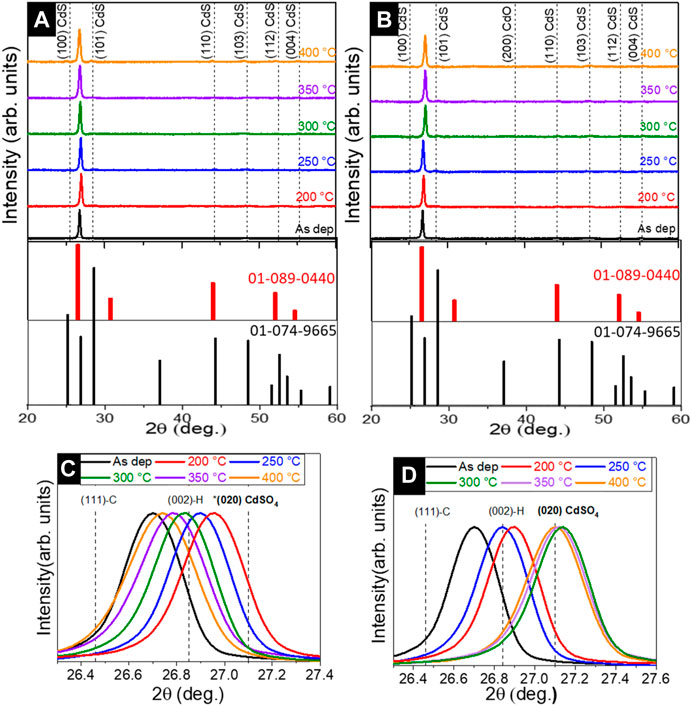
FIGURE 1. XRD pattern of (A) vacuum annealed and (B) air annealed CdS films, at 200°C–400°C temperatures for 30 min; displacement of dominant XRD peak depending on the (C) vacuum and (D) air annealing conditions.
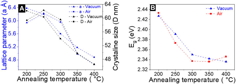
FIGURE 2. (A) variation of lattice parameter (A) and crystalline size (D) depending on the vacuum and air annealing temperatures. (B) variation in the bandgap of CdS films with vacuum and air annealing temperature.
The above observations related to the shift of the main XRD peak (corresponding changes in the lattice parameter), and appearance of oxide phases can be correlated considering the following aspects. First, the appearance of the CdO phase at higher annealing temperature (Figure 1B) has been observed previously in (Maticiuc et al., 2015) and explained by the decomposition of CdSO3 which is usually formed in the CdS lattice when reacting with oxygen in the air (Kylner, 1999; Maticiuc et al., 2014). The shifting of the main peak as a result of vacuum annealing can be related to the decomposition of Cd (OH)2 which naturally crystallized in the lattice during the deposition process of the CdS film. The presence of Cd (OH)2 in the CdS lattice is also the main reason for the variation of lattice (correspondingly shift of the main XRD peak) between the hexagonal and cubic structures. The increase in the annealing temperature generates the dissociation of Cd (OH)2 into CdO and water, and promotes the changes in the lattice parameters (Figure 3A). The reduction of lattice constants in both air and vacuum annealing conditions can be also explained due to mobility of (OH)s groups in the CdS lattice. A good indication of this effect is the decreasing of crystallite size as the temperature of vacuum and air annealing increased from 200°C to 400°C (Figure 2A). Although such a trend in the crystallite size with annealing temperature is an unexpected trend, the out-diffusion of OH impurity has such impact on the CdS lattice as explained in (Maticiuc et al., 2017). On the other hand, in the case of air-annealed samples, the position of the main XRD peak at 27.15° is very close to the 2-theta value of 020 diffraction peak position corresponding to the CdSO4 phase. The overall presence of phase mixture in CdS can play important role in the optoelectronic properties of CdS and related CdS/Sb2Se3 solar cell performance.
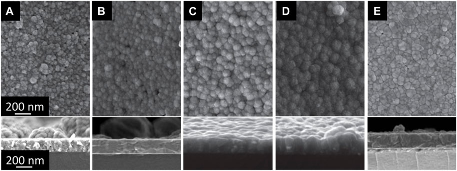
FIGURE 3. Surface and cross-section SEM images of CdS films deposited on glass substrates: (A) as deposited, (B) annealed in vacuum at 200°C, (C) annealed in air at 200°C, (D) annealed in vacuum at 400°C, (E) annealed in air at 400°C with an annealing duration of 30 min.
The morphology of as-deposited and annealed CdS films was also investigated by SEM. Figure 3 shows the surface and cross-section SEM images of CdS films deposited on glass substrates. As deposited CdS layer (Figure 3A) has small grains with some particles agglomerated in clusters. Vacuum annealing at 200°C did not change the grain size and overall morphology of the layers (Figure 3B). However, the same annealing temperature in the air leads to more uniform grain size distribution (Figure 3C). While vacuum annealing at 400°C lead to the similar morphology observed for the 200°C air annealing (Figure 3D), the same annealing at 400°C in the air lead to the more densely packed grains in the films (Figure 3E). The latest observation indicates that 400°C air annealing generates conditions for re-crystallization and sintering of the CdS films.
Since the CdS is deposited on FTO for the solar cell fabrication, the morphology of the CdS deposited on FTO substrates was also analyzed (Figure 4). As can be seen in Figures 4A, B, both, as deposited and 200°C vacuum annealed CdS films grown on FTO exhibit similar morphology with CdS deposited on glass. In this case, the porous layers comprising small grains and some grain conglomerates cover uniformly the relatively large FTO grains. Air annealing at 200°C and 400°C and as well as vacuum annealing at 400°C lead to significant densification of the CdS film (Figures 4C–E).
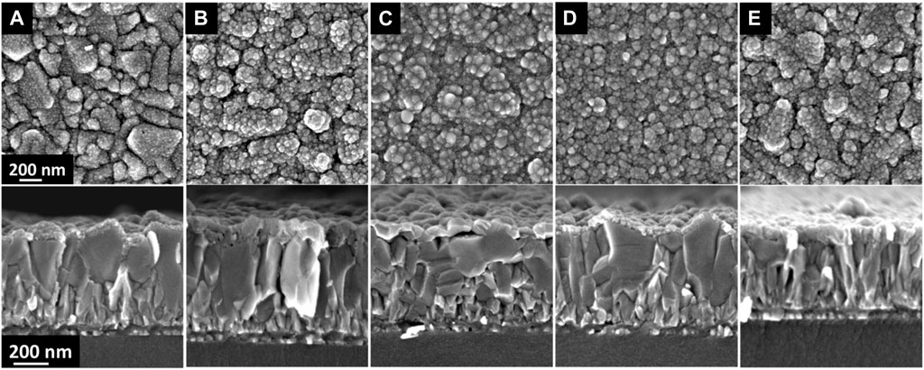
FIGURE 4. Surface and cross-section SEM images of CdS films deposited on FTO/glass substrates: (A) as deposited, (B) annealed in vacuum at 200°C, (C) annealed in air at 200°C, (D) annealed in vacuum at 400°C, (E) annealed in air at 400°C with an annealing duration of 30 min.
3.2 Impact of annealing conditions on CdS optoelectronic properties
The above results on the changes of structural and morphological properties of CdS films with annealing conditions will impact the optoelectronic properties of these layers and consequently will affect the solar cell performance. Thus, as a further step, a detailed analysis of changes in the electrical properties of the CdS layer depending on the annealing was performed.
Table 1 shows the variation of electrical properties (carrier concentration, mobility, and resistivity) of CdS films deposited on a glass substrate after post-deposition air and vacuum annealing at 200°C–400°C for 30 min. As deposited CdS films showed n-type conductivity with 4.4×1015 cm−3 carrier concentration, 5 cm2/Vs. mobility, and 2.8 × 10² Ω cm resistivity. All the films maintain the same conductivity type independent of the annealing conditions. For both air and vacuum annealing conditions, the variation of electrical parameters in Table 1 can be divided into three distinct regions: i) 200°C–250°C annealing in which the resistivity decreases from 4.2 to 2.6 Ω cm and from 3.2 to 0.2 Ω cm while the electron concentration increases by one order magnitude, from 1017 to 1018 cm−3 and 1018 to 1019 cm−3 for air and vacuum annealing, respectively; ii) 300°C annealing where resistivity increases to 45 and 8.5 Ω cm while the electron concentration decreases by one order of magnitude, from 1018 to 1017 cm−3 and from 1019 to 1018 cm−3 for air and vacuum annealing, respectively; iii) 350°C–400°C annealing where the resistivity increases from 7.7 × 10³ to 4.2 × 10⁴ Ω cm and 4.6 × 101 to 1 × 10⁴ Ω cm while the electron density reduces drastically by three and seven orders of magnitude for air and vacuum annealing, respectively. A similar trend in the electron concentration with the variation of air annealing temperature has been observed by Maticiuc et al. (Maticiuc et al., 2014) and correlated with the mobility of the hydroxide group (OH) in the CdS lattice. It has been proposed that the OH incorporated in the lattice of CdS, acting as a shallow donor (Varley and Lordi, 2013). At low annealing temperatures (200°C), the OH groups are quite unstable and decomposes by releasing water and generating sulfur vacancies (VS). It is well established that the sulfur vacancies (VS2+) act as a donor defect and an increase in their concentration can explain the abrupt increase in electron density. The high annealing temperatures (350°C and 400°C) induces conditions for excessive removal of OH from the CdS lattice, which results in the reduction of electron density. Although such mechanism was described for hydrogen and air-annealed CdS layers, it is also valid for vacuum annealing in this study. In addition to this mechanism, specifically for air annealing at 400°C, the presence of CdO secondary phases (as detected from XRD in Figure 1B) in CdS could be responsible for the significant drop in electron concentration to ∼1010 cm−3. The low values of mobilities at 200°C–300°C annealing temperature can be explained by the scattering of carriers with ionized impurities in the lattice. At higher air and vacuum annealing temperatures (350°C and 400°C) these impurities are removed from the lattice which leads to higher values of mobility(Spalatu et al., 2019).
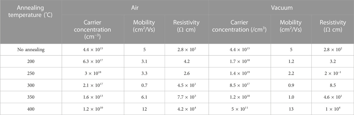
TABLE 1. Electrical properties of CdS films annealed at different annealing temperatures in air and vacuum.
The band gap of CdS films deposited on glass substrates was determined from a Tauc plot based on the UV—VIS measurements and the effect of annealing temperature and conditions on the bandgap values were analyzed thoroughly. As deposited CdS, films exhibit a band gap value of ∼2.42 eV. As the annealing temperature (200°C–400°C) in both air and vacuum increased a clear trend of band gap decrease was observed (Figure 2B). While for vacuum annealing this effect can be explained due to the decomposition of Cd (OH)2 to CdO and water (Maticiuc et al., 2014), in air annealing the presence of CdO (as detected by XRD) narrows the band gap (Dakhel, 2010).
3.3 Structure and morphology of Sb2Se3 films deposited on annealed CdS layer
As a step towards the fabrication of a solar cell device, Sb2Se3 absorber films were deposited on a glass/FTO/CdS stack and the impact of the CdS air and vacuum annealing on structure and morphology of Sb2Se3 films was analyzed.
Figures 5A, B shows the XRD patterns and texture coefficients of Sb2Se3 films grown on as-deposited, 200°C and 400°C air annealed, and 200, 400°C vacuum annealed CdS samples. Texture coeficients were performed according to (Krautmann et al., 2021). Diffraction peaks at 28.2°, 31.1°, 32.2°, 45.1°, and 45.6° were detected and comparing the patterns with standard data (JCPDS 15-0861) in both annealing conditions, it belongs to 211, 221, 301, 151, and 002 planes of orthorhombic Sb2Se3 crystal structure (Krautmann et al., 2021). In the Sb2Se3 films deposited on air-annealed CdS films, the grains grow predominantly along the (002) plane. The intensity of the (002) peak is dominant over the others, especially being highlighted for Sb2Se3 grown on 400°C air annealed CdS. Meanwhile, the Sb2Se3 grown on the vacuum annealed samples always exhibit 221 orientation. These results indicate that the Sb2Se3 tends to grow more vertically on the air-annealed CdS film compared to the vacuum-annealed CdS samples. Generally, there is no clear evidence for a preferential orientation in any of the Sb2Se3 samples. Although the intensity of 221 reflection is slightly higher for the Sb2Se3 absorber grown onto 400°C vacuum annealed CdS, it can be concluded that the samples are randomly oriented.
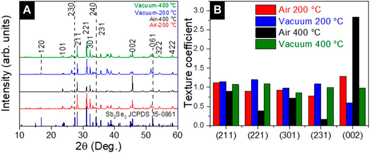
FIGURE 5. (A) XRD spectrum and (B) texture coefficient of Sb2Se3 on CdS annealed in vacuum and air at 200°C and 400°C.
One possible explanation for the 002 highlighted Sb2Se3 grain orientation deposited on 400°C air-annealed CdS might be related to the more compact grain morphology of CdS. As shown by SEM (Figure 3) these films with large sintered grains and higher surface energy can provide different nucleation sites favorable for the growth of Sb2Se3 in this direction. At the same time, oxidation of the layer (detection of CdO from XRD, Figure 1B) could also contribute to this effect, however, there is no direct proof for this hypothesis and specific investigation is required.
From a structural, optical, and morphological analysis of CdS, it was found that higher temperature (300°C–400°C) vacuum annealed CdS films have pin holes and lower band gap meanwhile in air annealed CdS films presence of impurities like CdO was detected in the film. Based on these findings a set of glass/FTO/CdS/Sb2Se3 heterostructures were analyzed by SEM. Figure 6 shows the surface and cross-section SEM images of CdS/Sb2Se3 with as-deposited, vacuum, and air annealed at 200°C CdS films. It can be seen that the absorber grown on as-deposited CdS (Figure 6A) exhibit more irregularly shaped grains with sharp edges and higher inner porosity compared to the Sb2Se3 films grown on annealed CdS. The absorber deposited on 200°C vacuum annealed CdS has larger, compact, and well-packed grains (Figure 6B). Air-annealed CdS at 200°C resulted in a similar well-packed absorber morphology with a more homogeneous distribution of grain shape and size. It is important to mention that the absorber deposited on both, 400°C vacuum and air-annealed CdS, displays similar morphology as seen in Figure 6C Overall the results of SEM analysis for the absorber are in good correlation with the above SEM and XRD results of CdS films. Thus, the reason for the higher inner porosity of the absorber in Figure 6A is related to the high concentration of organic residues in as-deposited CdS films. In this case, the subsequent CSS Sb2Se3 deposition process acts as an annealing process for the CdS films, resulting in the out-diffusion of organic residues from the films and making the absorber film porous and pinhole rich. On the other hand, in the annealed CdS films these residues are already removed from the CdS leading to more stable films which help the absorber to grow in a more pinhole-free compact manner.

FIGURE 6. SEM images of superstrate configuration glass/FTO/CdS/Sb2Se3 stack with CSS Sb2Se3 absorber layer deposited at 460°C: (A) top-and cross-sectional view of absorber film deposited onto as deposited CdS, (B) top-and cross-sectional view of absorber deposited onto vacuum annealed CdS at 200°C and (C) top-and cross-sectional view onto air annealed CdS at 200°C.
3.4 Impact of the CdS annealing on the device performance
The solar cells were fabricated following the superstrate configuration of glass/FTO/CdS/Sb2Se3/Au and the impact of the CdS annealing conditions on the PV parameters was analyzed. The PV parameters of the devices were extracted from the J–V curve measurements (Figure 8A representative curves under illumination) and the average values are presented in Figure 7. The analysis shows that the solar cells with as-deposited CdS exhibit the lowest PCE, whereas the devices with 200°C vacuum and air-annealed CdS buffer layer, there is a clear improvement in all the PV parameters (VOC, JSC, FF, and PCE). Nevertheless, all the PV parameters decreased for the cells with CdS annealed in both, vacuum and air at T ≥ 250°C. So far, comparing the performance of all the devices in Figure 7, it is clear that annealing of CdS at 200°C in both vacuum and air resulted in the best solar cells PCE, with the top performance of 2.8% (VOC of 350 mV, JSC of 18.3 mA/cm2 and fill factor of 43%) achieved for the cells processed with 200°C air annealed CdS (Table 2). The same best cell shows the highest EQE response in the short-wavelength region, 300–700 nm (Figure 8B). In caparison with the best cell, the EQE response in the 300–700 nm region is significantly reduced for the devices with as-deposited and 200°C vacuum annealed CdS. The reduced EQE response in the short-wavelength region has been previously observed for Sb2Se3/CdS (Phillips et al., 2019; Spalatu et al., 2021) and for CdTe/CdS devices (Potlog et al., 2012; Maticiuc et al., 2015; Spalatu et al., 2015) and explained by intermixing between CdS and Sb2Se3 (or CdTe) absorbers with the formation of CdS1-xSex (or CdTe1-xSx) solid alloy at the main interface. In the case of Sb2Se3 devices with as-deposited and 200°C vacuum annealed CdS this intermixing seems to be very pronounced resulting in low EQE response at 300–700 nm region. For the device with as-deposited CdS, this effect can be related to the morphology of CdS film, containing small grains (Figures 3A, 4A) with high surface energy, which are active for interdiffusion by mass transport through the gas phase, and resulting in a high degree of alloy formation at the interface during Sb2Se3 absorber deposition at 450°C. In addition to this effect, the presence of organic residuals (Graf et al., 2015; Maticiuc et al., 2015; Koltsov et al., 2022) and the presence of large segregates on the surface of as-deposited CdS can significantly alter the formation of the heterojunction interface resulting in reduced EQE and modest PCE of the corresponding solar cell (Figures 8A, B). On another hand, for the device with 200°C vacuum annealed CdS the improved EQE response (Figure 8B) and PCE (Figure 8A) (compared with as-deposited CdS-based cells) indicate the formation of better CdS-Sb2Se3 interface which can be connected with the removal of the organic residuals from CdS as a result of vacuum annealing, leading to better absorber morphology and better-quality interface. Finally, 200°C air annealing of CdS films resulted in the best EQE response and maximum device performance implying that intermixing in the corresponding cell has the lowest extent. For the same best device, the energy-band diagram with the band alignment was drawn (Figure 8E) based on photoelectron emission spectroscopy. The ionization potential (Ip) of the Sb2Se3 and CdS layers was determined through the extrapolation of the linear fit from valence band edge photoemission to 0 eV. An example of fitting for the absorber is presented in Figure 8C, obtaining an Ip value of 5.42 ± 0.02 eV, in good correlation with the values reported in the literature (Hobson et al., 2020). Further analysis of the band diagram shows that the conduction band minima of CdS lie above the conduction band minima of Sb2Se3, forming a spike-like band offset (∼0.2 eV) at the main interface. This spike-like band offset could act as a potential barrier for the electron flow which reduces the JSC of the device (Shiel et al., 2020). Furthermore, the linear extrapolation fit to 0 K in the VOC–T plot provides an activation energy of 0.98 ± 0.01 eV (Figure 8D), which is lower than the band gap of the absorber (∼1.2 eV). This implies that the rate of the recombination processes at the main interface is high, which reduces the PV parameters of the solar cell device. There are several recent reports in which the recombination of the carriers was suppressed by different techniques such as the introduction of Al3+ cations in the CdS buffer layer (Luo et al., 2023), heterojunction annealing (Tang et al., 2022), and effective antimony selenide crystal engineering (Tang et al., 2022).
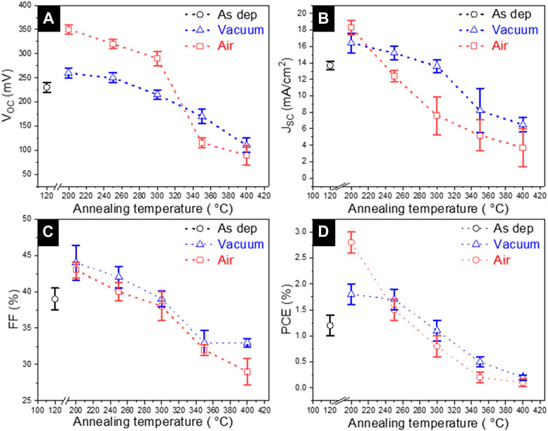
FIGURE 7. Main photovoltaic parameters including (A) open circuit voltage (VOC), (B) short circuit current density (JSC), (C) fill factor (FF), and (D) photoconversion efficiency (PCE) with average values (marked as hollow squares) measured for Sb2S3 devices with Sb2S3absorber deposited at substrate temperatures in the range of 240°C–400°C.
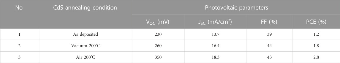
TABLE 2. Photovoltaic parameters of the best performing CdS/Sb2Se3 solar cells with as-deposited, vacuum and air annealed at 200°C, CdS films.
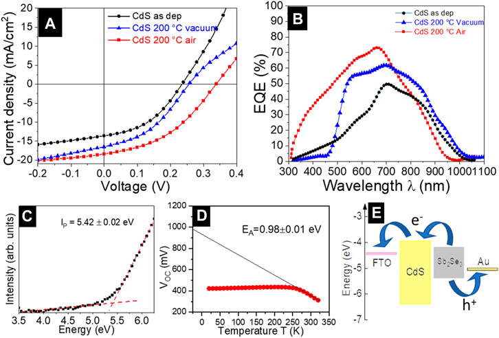
FIGURE 8. (A) J-V characteristics and (B) EQE of CdS/Sb2Se3 solar cells with as deposited, air and vacuum annealed CdS at 200°C, (C) Ionization potential of Sb2Se3 (D) activation energy calculated from VOC–T plot, (E) band alignment of FTO/CdS/Sb2Se3/Au solar cell structure.
So far the best PCE of 2.8% in this study was obtained for the device processed with CdS annealed at 200°C. The obtained result is significant from one side, considering a 60% boost in PCE compared to the cell fabricated with as-deposited CdS (1.8%). With this achievement, we also demonstrated that annealing in air at a relatively low temperature can be a suitable PDT to improve the properties of CdS films and the efficiency of the related device. On another side, putting in the context of other reports, these results could provide some more debates as several reports on similar device configurations suggested that an annealing step at temperatures ≥400°C and in the presence of air and CdCl2 treatment is a requirement for CdS to achieve PCE between 5%–7% (Wang et al., 2015; Li et al., 2018; Azam et al., 2022; Cai et al., 2022). Application of high air annealing temperature (400°C) in this study and attempts to perform post-deposition CdCl2 treatment of CdS films in our previous investigation (Spalatu et al., 2021) show that the oxide phases (and oxy-chloride residuals) which inevitably are formed at the surface CdS have a detrimental impact on the formation of good quality heterojunction interface and can significantly decrease the device performance. In addition, most of the studies that report a reasonable 5%–7% PCE for CdS/Sb2Se3 devices use thermal evaporation (TE) for deposition of the Sb2Se3 absorber (Liu et al., 2014; Kumar et al., 2019). Better control of the intermixing between CdS and Sb2Se3 may lead to better interfaces and higher PCE cells. Compared to TE, CSS employed in this study, clearly provide the advantage of the rapid process and high-quality absorber, however, the peculiarity of CSS with very close proximity between substrate and source (which implies high supersaturation of the vapor stream close to the substrate) can be a limitation for some device configuration which involve high reactivity of the underlayer components such as CdS. A prospective approach to overcome this challenge could be the implementation of various interfacial nanoscale layers such as TiO2 (the feasibility of CSS being well proven for Sb2Se3/TiO2 device configuration), which from one side, would imply more efforts for the interface engineering, and from a wider perspective, identification of other alternative partner layers with suitable band offsets for the emerging Sb2Se3 device.
4 Conclusion
In this study, we investigated the influence of air and vacuum annealing on the properties of CBD-deposited CdS films and find out the impact of these annealing conditions on the performance of CdS/Sb2Se3 solar cells. It was found that the increase of the annealing temperature from 200 to 400°C in both, vacuum and air ambient, changed the morphology of CdS from highly dispersed small grain structure to sintered dense grains, decreased the band gap from 2.43 to 2.35 eV and dropped the electron density from ∼1018 to ∼1011 cm−3. The changes in the properties of annealed CdS films were explained via the mechanism of the OH group in the lattice as well as the presence of secondary phases. The annealing conditions of CdS layers significantly impact the structural and morphological properties of the Sb2Se3 absorber. While the Sb2Se3 absorber grown on as-deposited CdS exhibited irregularly shaped grains with sharp edges and higher inner porosity, the absorber layers deposited on 200°C and 400°C vacuum annealed CdS have larger, compact, and well-packed grains. XRD analysis showed that Sb2Se3 tends to grow more vertically on the air-annealed CdS film compared to the vacuum-annealed CdS samples. 200°C air annealing of CdS was found as an optimal treatment resulting in 2.8% Sb2Se3/CdS cell PCE—a 60% boost compared to the 1.8% performance of the device with as deposited CdS. The performance of the CdS/Sb2Se3 solar cells has reduced as the annealing temperature increase in both, air and vacuum conditions. The presence of oxide phases in CdS annealed in air at 400°C is detrimental to the device’s performance. In addition, the extent of intermixing phenomenon between the CdS buffer layer and CSS Sb2Se3 absorber as well as intense carrier recombination at the main interface are the strong limiting factors for the PCE of CdS/Sb2Se3 solar cells.
Data availability statement
The raw data supporting the conclusion of this article will be made available by the authors, without undue reservation.
Author contributions
SV: Conceptualization, methodology, validation, formal analysis, investigation, writing—original draft, visualization. NS: Conceptualization, investigation, formal analysis, writing—review and editing, resources, supervision, project administration, funding acquisition. MB: Methodology, Investigation. RK: Writing—review and editing. AK: Investigation. RJ: Investigation, formal analysis. RG: Formal analysis, Investigation. AV: Formal analysis, Investigation. MK: Writing—review and editing. IO: Writing, reviewing and editing, project administration funding acquisition. All authors listed have made a substantial, direct, and intellectual contribution to the work and approved it for publication. All authors contributed to the article and approved the submitted version.
Funding
This study was funded by the Estonian Research Council projects PRG627 “Antimony chalcogenide thin films for next-generation semi-transparent solar cells applicable in electricity producing windows,” PSG689 “Bismuth Chalcogenide Thin-Film Disruptive Green Solar Technology for Next-Generation Photovoltaics,” the Estonian Centre of Excellence project TK141 (TAR16016EK) “Advanced materials and high-technology devices for energy recuperation systems,” and the European Union’s Horizon2020 programme under the ERA Chair project 5GSOLAR grant agreement No. 952509. The article/publication is based upon work from COST Action Research and International Networking on Emerging Inorganic Chalcogenides for Photovoltaics (RENEW-PV), CA21148, supported by COST (European Cooperation in Science and Technology). Institute of Solid-State Physics, University of Latvia has received funding from the European Union’s Horizon 2020 Framework Programme H2020-WIDESPREAD-01-2016-2017-TeamingPhase2 under grant agreement No. 739508, project CAMART2.
Conflict of interest
The authors declare that the research was conducted in the absence of any commercial or financial relationships that could be construed as a potential conflict of interest.
Publisher’s note
All claims expressed in this article are solely those of the authors and do not necessarily represent those of their affiliated organizations, or those of the publisher, the editors and the reviewers. Any product that may be evaluated in this article, or claim that may be made by its manufacturer, is not guaranteed or endorsed by the publisher.
References
Azam, M., Luo, Y., Tang, R., Chen, S., Zheng, Z. H., Su, Z. H., et al. (2022). Organic chloride salt interfacial modified crystallization for efficient antimony selenosulfide solar cells. ACS Appl. Mat. Interfaces 14, 4276–4284. doi:10.1021/acsami.1c20779
Büttner, P., Scheler, F., Döhler, D., Barr, M. K. S., Bosch, M., Rey, M., et al. (2022). Continuous, crystalline Sb2S3 ultrathin light absorber coatings in solar cells based on photonic concentric p-i-n heterojunctions. Nano Energy 103, 107820. doi:10.1016/j.nanoen.2022.107820
Cai, H., Cao, R., Gao, J., Qian, C., Che, B., Tang, R., et al. (2022). Interfacial engineering towards enhanced photovoltaic performance of Sb2Se3 solar cell. Adv. Funct. Mat. 32, 2208243. doi:10.1002/adfm.202208243
Campbell, S., Phillips, L. J., Major, J. D., Hutter, O. S., Voyce, R., Qu, Y., et al. (2022). Routes to increase performance for antimony selenide solar cells using inorganic hole transport layers. Front. Chem. 10, 954588. doi:10.3389/fchem.2022.954588
Carron, R., Nishiwaki, S., Feurer, T., Hertwig, R., Avancini, E., Löckinger, J., et al. (2019). Advanced alkali treatments for high-efficiency Cu(in,Ga)Se2 solar cells on flexible substrates. Adv. Energy. Mat. 9, 1900408. doi:10.1002/AENM.201900408
Chen, C., Li, W., Zhou, Y., Chen, C., Luo, M., Liu, X., et al. (2015). Optical properties of amorphous and polycrystalline Sb2Se3 thin films prepared by thermal evaporation. Appl. Phys. Lett. 107, 043905. doi:10.1063/1.4927741
Chen, S., Liu, T., Chen, M., Ishaq, M., Tang, R., Zheng, Z., et al. (2022). Crystal growth promotion and interface optimization enable highly efficient Sb2Se3 photocathodes for solar hydrogen evolution. Nano Energy 99, 107417. doi:10.1016/j.nanoen.2022.107417
Dakhel, A. A. (2010). Electrical and optical properties of iron-doped CdO. Thin Solid Films 518, 1712–1715. doi:10.1016/j.tsf.2009.11.026
Fan, P., Chen, G. J., Chen, S., Zheng, Z. H., Azam, M., Ahmad, N., et al. (2021). Quasi-vertically oriented Sb2Se3thin-film solar cells with open-circuit voltage exceeding 500 mV prepared via close-space sublimation and selenization. ACS Appl. Mat. Interfaces 13, 46671–46680. doi:10.1021/ACSAMI.1C13223/ASSET/IMAGES/ACSAMI.1C13223.SOCIAL.JPEG_V03
Graf, A., Maticiuc, N., Spalatu, N., Mikli, V., Mere, A., Gavrilov, A., et al. (2015). “Electrical characterization of annealed chemical-bath-deposited CdS films and their application in superstrate configuration CdTe/CdS solar cells,” in Thin solid films (Elsevier B.V.), 351–355. doi:10.1016/j.tsf.2014.11.003
Green, M. A., Dunlop, E. D., Hohl-Ebinger, J., Yoshita, M., Kopidakis, N., and Hao, X. (2021). Solar cell efficiency tables (Version 58). Prog. Photovoltaics Res. Appl. 29, 657–667. doi:10.1002/PIP.3444
Guo, H., Jia, X., Hadke, S. H., Zhang, J., Wang, W., Ma, C., et al. (2020). Highly efficient and thermally stable Sb 2 Se 3 solar cells based on a hexagonal CdS buffer layer by environmentally friendly interface optimization. J. Mat. Chem. C Mat. 8, 17194–17201. doi:10.1039/D0TC04017G
Guo, L., Grice, C., Zhang, B., Xing, S., Li, L., Qian, X., et al. (2019). Improved stability and efficiency of CdSe/Sb2Se3 thin-film solar cells. Sol. Energy 188, 586–592. doi:10.1016/j.solener.2019.06.042
Hernández-Calderón, V., Vigil-Galán, O., Guc, M., Carrillo-Osuna, A., Ramírez-Velasco, S., Sánchez-Rodríguez, F. J., et al. (2020). CdS/ZnS bilayer thin films used as buffer layer in 10%-efficient Cu2ZnSnSe4Solar cells. ACS Appl. Energy Mat. 3, 6815–6823. doi:10.1021/ACSAEM.0C00937/ASSET/IMAGES/ACSAEM.0C00937.SOCIAL.JPEG_V03
Hobson, T. D. C., Phillips, L. J., Hutter, O. S., Shiel, H., Swallow, J. E. N., Savory, C. N., et al. (2020). Isotype heterojunction solar cells using n-type Sb2Se3 thin films. Chem. Mat. 32, 2621–2630. doi:10.1021/acs.chemmater.0c00223
Koltsov, M., Krautmann, R., Katerski, A., Maticiuc, N., Krunks, M., Oja Acik, I., et al. (2022). A post-deposition annealing approach for organic residue control in TiO2 and its impact on Sb2Se3/TiO2 device performance. Faraday Discuss. 239, 273–286. doi:10.1039/d2fd00064d
Krautmann, R., Spalatu, N., Gunder, R., Abou-Ras, D., Unold, T., Schorr, S., et al. (2021). Analysis of grain orientation and defects in Sb 2 Se 3 solar cells fabricated by close-spaced sublimation. Sol. Energy 225, 494–500. doi:10.1016/j.solener.2021.07.022
Krautmann, R., Spalatu, N., Josepson, R., Nedzinskas, R., Kondrotas, R., Gržibovskis, R., et al. (2023). Low processing temperatures explored in Sb2S3 solar cells by close-spaced sublimation and analysis of bulk and interface related defects. Sol. Energy Mat. Sol. Cells 251, 112139. doi:10.1016/j.solmat.2022.112139
Kumar, V., Artegiani, E., Kumar, A., Mariotto, G., Piccinelli, F., and Romeo, A. (2019). Effects of post-deposition annealing and copper inclusion in superstrate Sb2Se3 based solar cells by thermal evaporation. Sol. Energy 193, 452–457. doi:10.1016/j.solener.2019.09.069
Kumar, V., Artegiani, E., Punathil, P., Bertoncello, M., Meneghini, M., Piccinelli, F., et al. (2021). Analysis of Se Co-evaporation and post-selenization for Sb2Se3-based solar cells. ACS Appl. Energy Mat. 4, 12479–12486. doi:10.1021/acsaem.1c02301
Kylner, A. (1999). Effect of impurities in the CdS buffer layer on the performance of the Cu(In, Ga)Se2 thin film solar cell. J. Appl. Phys. 85, 6858–6865. doi:10.1063/1.370204
Leng, M., Chen, C., Xue, D. J., Gong, J., Liu, Y., Li, K., et al. (2021). Sb2Se3 solar cells employing metal-organic solution coated CdS buffer layer. Sol. Energy Mat. Sol. Cells 225, 111043. doi:10.1016/J.SOLMAT.2021.111043
Li, D. B., Yin, X., Grice, C. R., Guan, L., Song, Z., Wang, C., et al. (2018). Stable and efficient CdS/Sb2Se3 solar cells prepared by scalable close space sublimation. Nano Energy 49, 346–353. doi:10.1016/j.nanoen.2018.04.044
Li, K., Chen, C., Lu, S., Wang, C., Wang, S., Lu, Y., et al. (2019a). Orientation engineering in low-dimensional crystal-structural materials via seed screening. Adv. Mat. 31, 1903914. doi:10.1002/adma.201903914
Li, Z., Chen, X., Zhu, H., Chen, J., Guo, Y., Zhang, C., et al. (2017). Sb2Se3 thin film solar cells in substrate configuration and the back contact selenization. Sol. Energy Mat. Sol. Cells 161, 190–196. doi:10.1016/J.SOLMAT.2016.11.033
Li, Z., Liang, X., Li, G., Liu, H., Zhang, H., Guo, J., et al. (2019b). 9.2%-efficient core-shell structured antimony selenide nanorod array solar cells. Nat. Commun. 10, 125. doi:10.1038/s41467-018-07903-6
Liu, D., Tang, R., Ma, Y., Jiang, C., Lian, W., Li, G., et al. (2021). Direct hydrothermal deposition of antimony triselenide films for efficient planar heterojunction solar cells. ACS Appl. Mat. Interfaces 13, 18856–18864. doi:10.1021/ACSAMI.1C02393/SUPPL_FILE/AM1C02393_SI_001.PDF
Liu, X., Chen, J., Luo, M., Leng, M., Xia, Z., Zhou, Y., et al. (2014). Thermal evaporation and characterization of Sb2Se3 thin film for substrate Sb2Se3/CdS solar cells. ACS Appl. Mat. Interfaces 6, 10687–10695. doi:10.1021/am502427s
Luo, Y., Chen, G., Chen, S., Ahmad, N., Azam, M., Zheng, Z., et al. (2023). Carrier transport enhancement mechanism in highly efficient antimony selenide thin-film solar cell. Adv. Funct. Mat. 33. doi:10.1002/adfm.202213941
Maticiuc, N., Katerski, A., Danilson, M., Krunks, M., and Hiie, J. (2017). XPS study of OH impurity in solution processed CdS thin films. Sol. Energy Mat. Sol. Cells 160, 211–216. doi:10.1016/j.solmat.2016.10.040
Maticiuc, N., Kukk, M., Spalatu, N., Potlog, T., Krunks, M., Valdna, V., et al. (2014). Comparative study of CdS films annealed in neutral, oxidizing and reducing atmospheres. Energy Procedia 44, 77–84. doi:10.1016/j.egypro.2013.12.012
Maticiuc, N., Spalatu, N., Mikli, V., and Hiie, J. (2015). “Impact of CdS annealing atmosphere on the performance of CdS-CdTe solar cell,” in Appl. Surf. Sci. (Elsevier B.V.), 14–18. doi:10.1016/j.apsusc.2015.01.172
Ou, C., Shen, K., Li, Z., Zhu, H., Huang, T., and Mai, Y. (2019). Bandgap tunable CdS:O as efficient electron buffer layer for high-performance Sb2Se3 thin film solar cells. Sol. Energy Mat. Sol. Cells 194, 47–53. doi:10.1016/J.SOLMAT.2019.01.043
Phillips, L. J., Savory, C. N., Hutter, O. S., Yates, P. J., Shiel, H., Mariotti, S., et al. (2019). Current enhancement via a TiO 2 window layer for CSS Sb 2 Se 3 solar cells: Performance limits and high V oc. IEEE J. Photovolt. 9, 544–551. doi:10.1109/JPHOTOV.2018.2885836
Potlog, T., Spalatu, N., Fedorov, V., Maticiuc, N., Antoniuc, C., Botnariuc, V., et al. (2011). “The performance of thin film solar cells employing photovoltaic ZnSe/CdTe, CdS/CdTe and ZnTe/CdTe heterojunctions,” in Conference Record of the IEEE Photovoltaic Specialists Conference, 001365–001370. doi:10.1109/PVSC.2011.6186211
Potlog, T., Spalatu, N., Maticiuc, N., Hiie, J., Valdna, V., Mikli, V., et al. (2012). Structural reproducibility of CdTe thin films deposited on different substrates by close space sublimation method. Phys. Status Solidi (A) Appl. Mater. Sci. 209, 272–276. doi:10.1002/pssa.201127123
Punathil, P., Zanetti, S., Artegiani, E., Kumar, V., and Romeo, A. (2021). Analysis of the drying process for precursors of Cu2ZnSn(S,Se)4 layers by low cost non vacuum fabrication technique. Sol. Energy 224, 992–999. doi:10.1016/J.SOLENER.2021.06.063
Shiel, H., Hutter, O. S., Phillips, L. J., Swallow, J. E. N., Jones, L. A. H., Featherstone, T. J., et al. (2020). Natural band alignments and band offsets of Sb2Se3Solar cells. ACS Appl. Energy Mat. 3, 11617–11626. doi:10.1021/acsaem.0c01477
Spalatu, N., Hiie, J., Kaupmees, R., Volobujeva, O., Krustok, J., Acik, I. O., et al. (2019). Postdeposition processing of SnS thin films and solar cells: Prospective strategy to obtain large, sintered, and doped SnS grains by recrystallization in the presence of a metal halide flux. ACS Appl. Mat. Interfaces 11, 17539–17554. doi:10.1021/acsami.9b03213
Spalatu, N., Hiie, J., Mikli, V., Krunks, M., Valdna, V., Maticiuc, N., et al. (2015). “Effect of CdCl2annealing treatment on structural and optoelectronic properties of close spaced sublimation CdTe/CdS thin film solar cells vs deposition conditions,” in Thin solid films (Elsevier B.V.), 128–133. doi:10.1016/j.tsf.2014.11.066
Spalatu, N., Krautmann, R., Katerski, A., Karber, E., Josepson, R., Hiie, J., et al. (2021). Screening and optimization of processing temperature for Sb2Se3 thin film growth protocol: Interrelation between grain structure, interface intermixing and solar cell performance. Sol. Energy Mat. Sol. Cells 225, 111045. doi:10.1016/j.solmat.2021.111045
Spalatu, N., Krunks, M., and Hiie, J. (2017). Structural and optoelectronic properties of CdCl2 activated CdTe thin films modified by multiple thermal annealing. Thin Solid Films 633, 106–111. doi:10.1016/j.tsf.2016.09.042
Tang, R., Chen, S., Zheng, Z. H., Su, Z. H., Luo, J. T., Fan, P., et al. (2022). Heterojunction annealing enabling record open-circuit voltage in antimony triselenide solar cells. Adv. Mat. 34, 2109078. doi:10.1002/adma.202109078
Tang, R., Zheng, Z. H., Su, Z. H., Li, X. J., Wei, Y. D., Zhang, X. H., et al. (2019). Highly efficient and stable planar heterojunction solar cell based on sputtered and post-selenized Sb2Se3 thin film. Nano Energy 64, 103929. doi:10.1016/j.nanoen.2019.103929
Tiwari, K. J., Neuschitzer, M., Espíndola-Rodriguez, M., Sánchez, Y., Jehl, Z., Vidal-Fuentes, P., et al. (2020). Efficient Sb2Se3/CdS planar heterojunction solar cells in substrate configuration with (hk0) oriented Sb2Se3 thin films. Sol. Energy Mat. Sol. Cells 215, 110603. doi:10.1016/j.solmat.2020.110603
Varley, J. B., and Lordi, V. (2013). Electrical properties of point defects in CdS and ZnS. Appl. Phys. Lett. 103, 102103. doi:10.1063/1.4819492
Wang, L., Li, D. B., Li, K., Chen, C., Deng, H. X., Gao, L., et al. (2017). Stable 6%-efficient Sb2Se3 solar cells with a ZnO buffer layer. Nat. Energy 2, 17046. doi:10.1038/nenergy.2017.46
Wang, L., Luo, M., Qin, S., Liu, X., Chen, J., Yang, B., et al. (2015). Ambient CdCl2 treatment on CdS buffer layer for improved performance of Sb2Se3 thin film photovoltaics. Appl. Phys. Lett. 107, 143902. doi:10.1063/1.4932544
Wang, W., Cao, Z., Wu, L., Chen, G., Ao, J., Luo, J., et al. (2022). Interface etching leads to the inversion of the conduction band offset between the CdS/Sb 2 Se 3 heterojunction and high-efficient Sb 2 Se 3 solar cells. ACS Appl. Energy Mat. 5, 2531–2541. doi:10.1021/ACSAEM.1C04078/SUPPL_FILE/AE1C04078_SI_001.PDF
Weiss, T. P., Minguez-Bacho, I., Zuccalà, E., Melchiorre, M., Valle, N., el Adib, B., et al. (2022). Post-deposition annealing and interfacial atomic layer deposition buffer layers of Sb2Se3/CdS stacks for reduced interface recombination and increased open-circuit voltages. Prog. Photovoltaics Res. Appl. 31, 203–219. doi:10.1002/pip.3625
Wen, X., Chen, C., Lu, S., Li, K., Kondrotas, R., Zhao, Y., et al. (2018). Vapor transport deposition of antimony selenide thin film solar cells with 7.6% efficiency. Nat. Commun. 9, 2179–2210. doi:10.1038/s41467-018-04634-6
Zhou, J., Zhang, X., Chen, H., Tang, Z., Meng, D., Chi, K., et al. (2020). Dual-function of CdCl2 treated SnO2 in Sb2Se3 solar cells. Appl. Surf. Sci. 534, 147632. doi:10.1016/j.apsusc.2020.147632
Keywords: antimony selenide, close-spaced sublimation, cadmium sulfide, post deposition annealing, thin film solar cells
Citation: Vadakkedath Gopi S, Spalatu N, Basnayaka M, Krautmann R, Katerski A, Josepson R, Grzibovskis R, Vembris A, Krunks M and Oja Acik I (2023) Post deposition annealing effect on properties of CdS films and its impact on CdS/Sb2Se3 solar cells performance. Front. Energy Res. 11:1162576. doi: 10.3389/fenrg.2023.1162576
Received: 16 February 2023; Accepted: 28 April 2023;
Published: 10 May 2023.
Edited by:
Kok-Keong Chong, Tunku Abdul Rahman University, MalaysiaReviewed by:
Soonmin Ho, INTI International University, MalaysiaGuangxing Liang, Shenzhen University, China
Copyright © 2023 Vadakkedath Gopi, Spalatu, Basnayaka, Krautmann, Katerski, Josepson, Grzibovskis, Vembris, Krunks and Oja Acik. This is an open-access article distributed under the terms of the Creative Commons Attribution License (CC BY). The use, distribution or reproduction in other forums is permitted, provided the original author(s) and the copyright owner(s) are credited and that the original publication in this journal is cited, in accordance with accepted academic practice. No use, distribution or reproduction is permitted which does not comply with these terms.
*Correspondence: Sajeesh Vadakkedath Gopi, sajeesh.vadakkedath@taltech.ee; Nicolae Spalatu, nicolae.spalatu@taltech.ee