Study on the CM EMI Generation Characteristics of the Si/SiC Hybrid Switch at Different Switching Patterns and Gate Resistors
 Yong Zhu1
  Zijie Zheng
- 1Shenzhen Jingquanhua Electronics Co., Ltd., Shenzhen, China
- 2National-Local Joint Engineering Laboratory of Digitalize Electrical Design Technology, Wenzhou University, Wenzhou, China
- 3College of Electrical and Information Engineering, Hunan Institute of Engineering, Xiangtan, China
The switching patterns and gate resistor of the Si/SiC hybrid switch are the key to realizing its own highly efficient and reliable operation. However, as an important performance indicator, the common mode (CM) electromagnetic interference (EMI) noise caused by the Si/SiC hybrid switch lacks comprehensive research, which means that it is not clear how the switching patterns and gate resistor affect CM EMI. In this paper, the Si/SiC hybrid switch-based boost converter is established at first. Then, by analyzing the spectral characteristics of the CM voltage of the Si/SiC hybrid switch, the CM EMI generation characteristics of the Si/SiC hybrid switch at different switching patterns and gate resistors are revealed. Furthermore, the analysis and experimental results can be used to comprehensively guide the design of the gate drive pattern, gate resistor, and EMI suppression strategy.
1 Introduction
The hybrid structure comprising a Si IGBT and a SiC MOSFET in parallel, which is called the Si/SiC hybrid switch, was first proposed in 1993 (Jiang et al., 1993). With the help of the higher switching speed of the SiC MOSFET and the lower cost of the Si IGBT, the Si/SiC hybrid switch is proved to be promising in the application of power converters (Rahimo et al., 2015; Song and Huang, 2015). Switching patterns and gate resistors are the two important factors that can change the switching speed of the Si/SiC hybrid switch and the conduction time of each device inside the Si/SiC hybrid switch, which can directly affect its own power loss (Minamisawa et al., 2016; Li et al., 2019; Peng et al., 2020). Meanwhile, the dv/dt of the Si/SiC hybrid switch can be changed by its own switching speed, resulting in the variation of the conducted electromagnetic interference (EMI) generation in the application of the power converters. Because the CM EMI issue is one of the big concerns in the design of Si/SiC hybrid switch-based power converters, corresponding research is necessary (Gong et al., 2012; Roscoe et al., 2015; Han et al., 2017a; Zhang et al., 2017; Du et al., 2021).
In recent years, in order to improve the performance and reliability of Si/SiC hybrid switch-based power converters, the reported research studies on the Si/SiC hybrid switch have been focused on the loss, junction temperature, and reliability issue of the overcurrent (Oswald et al., 2014; Huang et al., 2015; Zhao and He, 2015; He et al., 2017; Ueno et al., 2017; Li et al., 2018a; Li et al., 2018b; Li et al., 2018c; He et al., 2018). In (Oswald et al., 2014; Huang et al., 2015; Ueno et al., 2017; Li et al., 2018a; Li et al., 2018c), the switching pattern, switching delay time, and gate resistor of the Si MOSFET and Si IGBT were studied to achieve low loss of the Si/SiC hybrid switch. In (Li et al., 2018b; He et al., 2018), the junction temperature balance of the Si/SiC hybrid switch can be achieved by the optimal delay time or integrated gate driver. Furthermore, these methods can also prevent the junction temperature of the SiC MOSFET from getting too high. In (Zhao and He, 2015; He et al., 2017; Liu et al., 2019), a current-dependent switching strategy is proposed to improve the reliability of the SiC MOSFET inside the Si/SiC hybrid switch when the inverters operate under a heavy load condition. However, the studies of the CM EMI caused by the Si/SiC hybrid switch is neglected by these researchers, which means that the design of high-performance and high-reliability power converters is not considered comprehensively. In fact, CM EMI is one of the most important factors affecting the reliability of power converters (Oswald et al., 2011; Domurat-Linde et al., 2012; Ji et al., 2015; Cui et al., 2017); the study of the CM EMI noise caused by the Si/SiC hybrid switch is desired.
Until now, the mechanism study of the CM EMI noise caused by the Si/SiC hybrid switch is still in its infancy. In (Deshpande and Luo, 2019), researchers have simply studied the CM EMI generation characteristics of the Si/SiC hybrid switch-based boost converter at two different switching patterns. However, there are four different switching patterns; each of these switching patterns will change the switching characteristics of the Si/SiC hybrid switch. Meanwhile, different delay times inside these switching patterns will also bring different switching characteristics. Therefore, the analysis of the CM EMI noise in this article is uncomprehensive. In (Minamisawa et al., 2016), the effect of the gate resistor on CM EMI is briefly mentioned when the Si/SiC hybrid switch is adopted. However, there is lack of detailed theoretical and experimental analysis about the relationship between the gate resistor and CM EMI generation characteristics. In conclusion, in order to guide the design of switching patterns and gate resistors in the application of Si/SiC hybrid switch-based power converters, comprehensive research about the CM EMI caused by the Si/SiC hybrid switch is important and necessary.
In this paper, in order to solve the above problems, the CM EMI generation characteristics of the Si/SiC hybrid switch-based boost converter at different switching patterns and gate resistors are analyzed. First, the spectral envelope equation of the CM voltage of the Si/SiC hybrid switch is obtained. Then, the switching characteristics of the Si/SiC hybrid switch at different switching patterns and gate resistors are analyzed. Meanwhile, the spectral envelope of the CM voltage is analyzed to predict the CM EMI noise caused by the Si/SiC hybrid switch at different switching patterns and gate resistors. Finally, the corresponding experiments are provided to verify the theory.
The rest of this paper is organized as follows. In CM EMI Analysis of the Si/SiC Hybrid Switch-Based Boost Converter, the structure of the Si/SiC hybrid switch-based boost converter is presented. Then, the spectral function of the CM voltage of the Si/SiC hybrid switch is established. In Experimental Results, the influence of the Si/SiC hybrid switch at different switching patterns and gate resistors on the CM EMI noise is analyzed. In Discussion, spectrum analysis based on CM voltage and the corresponding CM electromagnetic interference experiment are given. Conclusion concludes the paper.
2 CM EMI Analysis of Si/SiC Hybrid Switch Based Boost Converter
In this section, the interference propagation path of the Si/SiC hybrid switch-based boost converter is analyzed at first. Then, the spectral characteristics of the CM voltage of the Si/SiC hybrid switch are analyzed. Meanwhile, the CM EMI noise caused by the switching pattern and gate resistor is explained. Details are shown as follows.
2.1 Interference Propagation Path of Si/SiC Hybrid Switch Based Boost Converter
In this paper, the Si/SiC hybrid switch is configured by a Si IGBT [IGW25N120H3, 1200V/25A at 100°C (Infineon, 2019)] and a SiC MOSFET [C2M0160120D, 1200V/12.5A at 100°C (Rohm, 2019)] in parallel. The structure of the Si/SiC hybrid switch-based boost converter is shown in Figure 1. As can be seen from Figure 1, Uin, Uout, Cin, Cout, L, R, Sn1, and D1 represent the input voltage, output voltage, capacitor of the input terminal, capacitor of the output terminal, inductor, load, Si/SiC hybrid switch, and SiC SBD, respectively. CSiC,D1-H, CIGBT,C1-H, and CH-G represent the parasitic CM capacitance between the drain of the SiC MOSFET and heat sink, parasitic CM capacitance between the collector of the Si IGBT and heat sink, and parasitic CM capacitance between the heat sink and ground, respectively. In addition, GSiC, GSi, Rg_SiC, and Rg_Si represent the gate drive signal of the SiC MOSFET, gate drive signal of the Si IGBT, gate resistor of the SiC MOSFET, and gate resistor of the Si IGBT, respectively. As a major source of interference, the Si/SiC hybrid switch will propagate the CM EMI noise through the parasitic capacitors. Moreover, the corresponding propagation path is Si/SiC hybrid switch → CM capacitance between the collector of the Si IGBT/SiC MOSFET and heat sink → heat sink → CM capacitance between the heat sink and ground → ground → LISN → Si/SiC hybrid switch.
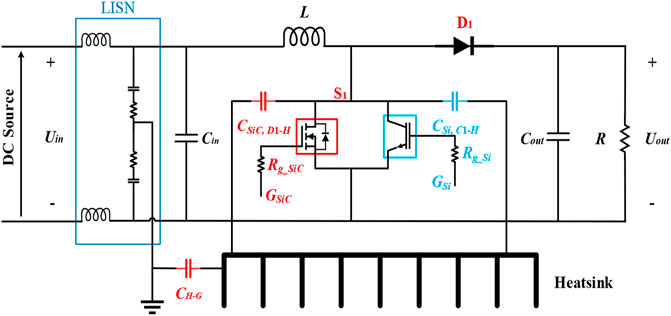
FIGURE 1. Structure of the Si/SiC hybrid switch-based boost converter.
According to the above analysis, the value of the CM current is affected by the value of the CM capacitance, the structure and material of the radiator, and the switching characteristics of the Si/SiC hybrid switch. For the Si/SiC hybrid switch, the CM capacitance of the Si/SiC hybrid switch consists of CSiC,D1-H and CIGBT,C1-H, which means that the switching patterns, delay time, and gate resistor of the Si/SiC hybrid switch can change the CM EMI noise. In this paper, the Si/SiC hybrid switch is the main interference source of the boost converter, so the CM EMI noise that is affected by the switching characteristics of the Si/SiC hybrid switch is considered.
2.2 Analysis of Spectral Characteristics of CM Voltage
In order to avoid the influence of the DC source on the CM EMI analysis of the Si/SiC hybrid switch-based boost converter, the line impedance stabilization network (LISN) is connected between the DC source and boost converter. The Si/SiC hybrid switch is the interference source in the boost converter; its switching waveform is the fundamental element of CM voltage, which can directly reflect the variation characteristics of the CM EMI (Kim et al., 2017). In fact, the CM voltage of the Si/SiC hybrid switch can be equivalent to an asymmetrical trapezoid, which is illustrated in Figure 2. In Figure 2, A, tr, tf, and τ represent the amplitude, rise time, fall time, and pulse width of the CM voltage, respectively. In order to better explain the CM EMI noise caused by the Si/SiC hybrid switch, spectral analysis of the CM voltage is necessary. According to the Fourier series, the Fourier coefficient in the asymmetrical trapezoidal waveform is written as (Igarashi et al., 2007; Qi et al., 2010; Han et al., 2017b; Fang et al., 2018).
where
In (1) and (2), fh and fs represent the harmonic frequency and switching frequency, respectively. There are fs = 1/Ts and fh = n/Ts (n = 1, 3, 5, … ). Meanwhile, the coefficient D represents the duty cycle. According to (1), there are three kinds of methods for changing the spectral characteristics of the CM voltage in the frequency range of 150 kHz–30 MHz.
1) As the rise time or fall time increases, the value of the Fourier coefficient will be reduced, which means that the spectrum amplitude of the CM voltage in the frequency range of 1/tr or 1/tf to 30 MHz will be reduced. In addition, if the rise time or fall time is decreased, the spectrum amplitude of the CM voltage in the frequency range of 1/tr or 1/tf to 30 MHz will be increased.
2) As the duty cycle increases, the spectrum amplitude of the CM voltage in the frequency range of 150 kHz–30 MHz will be reduced. Conversely, the spectrum amplitude of the CM voltage will be increased.
3) As the switching frequency increases, the spectrum amplitude of the CM voltage will be increased. In addition, the spectrum amplitude of the CM voltage will be reduced with the decrease in the switching frequency.
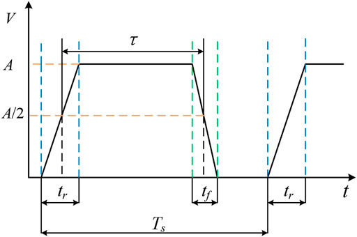
FIGURE 2. Asymmetrical trapezoid representing the CM voltage of the Si/SiC hybrid switch (Han et al., 2017b).
In conclusion, the CM EMI noise can be effectively changed by changing the switching speed and pulse width of the Si/SiC hybrid switch.
2.3 Analysis of the CM EMI Noise Caused by Switching Pattern and Gate Resistor
There are four different switching patterns for the Si/SiC hybrid switch, which will change its own switching speed, so the CM EMI noise caused by the Si/SiC hybrid switch will be affected by its own switching pattern. Meanwhile, the gate resistor in the Si/SiC hybrid switch will also affect the CM EMI noise by changing the switching speed. This section will analyze how different switching patterns and gate resistors affect the CM EMI noise. Details are shown as follows.
2.3.1 Analysis of Switching Pattern
The switching patterns of the Si/SiC hybrid switch are shown in Figure 3. As can be seen from Figure 3, Ton_delay and Toff_delay represent the turn-on delay time and turn-off delay time between the Si IGBT and SiC MOSFET, respectively. There are four different switching patterns for the Si/SiC hybrid switch, and details about how the influence of different switching patterns on the CM EMI noise are presented as follows.
Pattern 1: Si IGBT is turned on earlier and turned off later
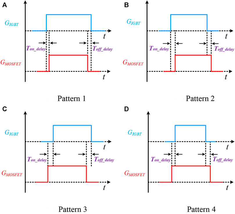
FIGURE 3. Switching patterns of the Si/SiC hybrid switch. (A) Pattern 1, (B) pattern 2, (C) pattern 3, and (D) pattern 4.
In this switching pattern, no matter how Toff_delay is changed, the turn-off characteristic of the Si/SiC hybrid switch always reflects the turn-off characteristic of the Si IGBT, which means that the influence of Toff_delay on the switching speed is too small to be considered. Therefore, only Ton_delay should be considered. The CM voltage waveforms of the Si/SiC hybrid switch under different Ton_delay are shown in Figure 4A. As can be seen from Figure 4A, the Si/SiC hybrid switch will reflect the turn-on characteristic of the SiC MOSFET when Ton_delay is small, while its turn-on speed will be gradually reduced (the fall time of the CM voltage will be increased) with the increase in Ton_delay. This means that the CM EMI noise caused by the Si/SiC hybrid switch will be reduced. However, when the turn-on speed of the Si/SiC hybrid switch is close to that of the Si IGBT, even when Ton_delay is further increased, its turn-on speed will not be obviously changed, which means that the CM EMI noise will not be obviously changed.
Pattern 2: Si IGBT is turned on and turned off earlier
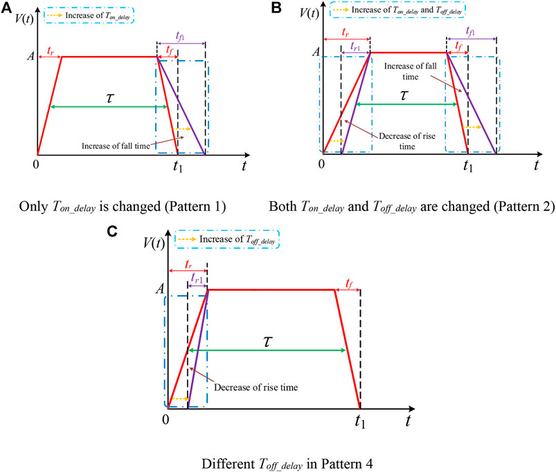
FIGURE 4. CM voltage waveforms of the Si/SiC hybrid switch. (A) Only Ton_delay is changed (pattern 1), (B) both Ton_delay and Toff_delay are changed (pattern 2), and (C) different Toff_delay in pattern 4.
The switching speed of the Si/SiC hybrid switch adopting this switching pattern is affected by Ton_delay or Toff_delay. When Ton_delay and Toff_delay are increased simultaneously, the CM voltage waveform of the Si/SiC hybrid switch under different Ton_delay is shown in Figure 4B. As can be seen from Figure 4A, when Ton_delay and Toff_delay are small, the Si/SiC hybrid switch reflects the turn-on characteristic of the SiC MOSFET and turn-off characteristic of the Si IGBT. As Ton_delay and Toff_delay increase simultaneously, the turn-on speed of the Si/SiC hybrid switch will be gradually reduced (the fall time of the CM voltage will be increased), and its turn-off speed will be gradually increased (the rise time of the CM voltage will be decreased), resulting in the variation of the CM EMI noise. However, the CM EMI noise caused by the Si/SiC hybrid switch will not be obviously changed when its turn-on speed is close to that of the Si IGBT and its turn-off speed is close to that of the SiC MOSFET. The CM EMI noise caused by the Si/SiC hybrid switch at different Ton_delay and Toff_delay will be discussed in the following experiments.
Pattern 3: SiC MOSFET is turned on and turned off earlier
In this switching pattern, no matter how Ton_delay and Toff_delay are changed, the turn-on characteristic of the Si/SiC hybrid switch always reflects the turn-on characteristic of the SiC MOSFET, and its turn-off characteristic always reflects the turn-off characteristic of the Si IGBT, which means that the CM EMI noise is almost not affected by Ton_delay and Toff_delay. In fact, pattern 3 is the special switching pattern of pattern 1, pattern 2, and pattern 4, so this switching pattern is not separately discussed in this paper.
Pattern 4: SiC MOSFET is turned on earlier and turned off later
In this switching pattern, the influence of Ton_delay on the turn-on characteristic of the Si/SiC hybrid switch is unchanged. Therefore, only Toff_delay should be considered. The CM voltage waveforms of the Si/SiC hybrid switch under different Toff_delay are shown in Figure 4C. As can be seen from Figure 4C, the Si/SiC hybrid switch will reflect the turn-off characteristic of the Si IGBT when Toff_delay is small, while its turn-off speed will be gradually increased (the rise time of the CM voltage will be decreased) with the increase in Toff_delay, which means that the CM EMI noise will be increased. In fact, when the turn-off speed of the Si/SiC hybrid switch is close to that of the SiC MOSFET, with a further increase in Toff_delay, the CM EMI noise will not be obviously changed.
Because the turn-on speed and turn-off speed of pattern 4 is faster than those of the other three patterns, the EMI noise caused by pattern 4 is worse than that of patterns 1 and 2. In addition, according to the above analysis, only pattern 1, pattern 2, and pattern 4 are considered in the following theoretical analysis.
2.3.2 Analysis of Gate Resistor
1) Gate resistors of the Si IGBT and SiC MOSFET are changed simultaneously
The CM voltage waveforms of the Si/SiC hybrid switch under different gate resistors are shown in Figure 5. As can be seen from Figure 5, as all the gate resistors (Rg_Si and Rg_SiC) increase, the switching speed of the Si/SiC hybrid switch at all switching patterns will be gradually reduced, which means that the rise time and fall time of the CM voltage at all switching patterns will be gradually decreased. Therefore, the CM EMI noise will be reduced.
2) Gate resistors of the Si IGBT and SiC MOSFET are changed independently
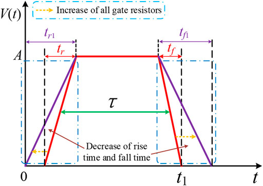
FIGURE 5. CM voltage waveforms of the Si/SiC hybrid switch.
When pattern 1 is adopted, as the gate resistor of the Si IGBT increases, the switching speed of the Si/SiC hybrid switch will be reduced. This means that the CM EMI noise caused by the Si/SiC hybrid switch will be reduced. When Ton_delay is large enough, as the gate resistor of the SiC MOSFET increases, the switching speed of the Si/SiC hybrid switch will not be changed, which means that the CM EMI noise caused by the Si/SiC hybrid switch will be unchanged.
When pattern 2 is adopted, whether the gate resistor of the Si IGBT or SiC MOSFET is increased, the CM EMI noise will be reduced.
When pattern 4 is adopted, as the gate resistor of the SiC MOSFET increases, the switching speed of the Si/SiC hybrid switch will also be reduced. This means that the CM EMI noise caused by the Si/SiC hybrid switch will be reduced. When Toff_delay is large enough, as the gate resistor of the Si IGBT increases, the switching speed of the Si/SiC hybrid switch will not be changed, which means that the CM EMI noise will be unchanged.
3 Experimental Results
In order to analyze the CM EMI generation characteristics of the Si/SiC hybrid switch-based boost converter at different switching patterns and gate resistors, the corresponding experimental platform is established, which is shown in Figure 6. As can be seen from Figure 6, it comprises a personal computer (PC), a DSP controller, a boost converter, a LISN, a spectrum analyzer, and a load box, and the experimental parameters are described in Table 1. Details about the CM EMI noise analysis and experiments at different switching patterns and gate resistors are presented as follows.
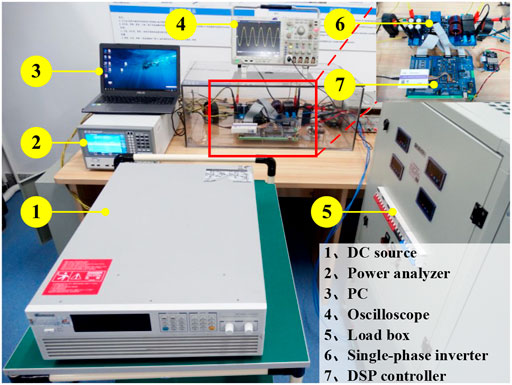
FIGURE 6. Experimental platform.
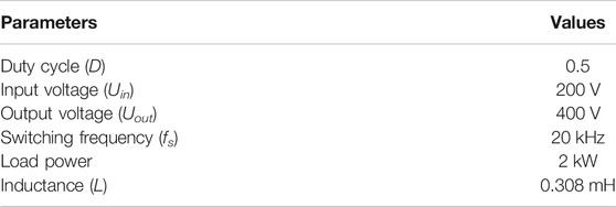
TABLE 1. Parameters of the experimental platform.
3.1 Experimental Results of Pattern 1 (Different Ton_delay)
In this condition, when Ton_delay is changed from 0us to 3us and Toff_delay is set as 0us, the waveforms of the CM voltage and its spectral envelope at different Ton_delay are shown in Figure 7. As can be seen from Figure 7A, the turn-off characteristic of the Si/SiC hybrid switch always reflects the turn-off characteristic of the Si IGBT, and its turn-on characteristic reflects the turn-on characteristic of the SiC MOSFET when Ton_delay is set as 0us. When Ton_delay is increased from 0us to 3us, the fall time of the CM voltage will be increased, and the spectral envelope in the frequency range of 1–30 MHz will be decreased by 0∼6 dB, which is shown in Figure 7B. In fact, when Ton_delay is increased from 1us to 3us, the Si/SiC hybrid switch always reflects the turn-on characteristic of the Si IGBT, which means that the spectral envelope is almost unchanged. Therefore, when Ton_delay is increased from 1us to 3us, the EMI noise characteristics will be unchanged.
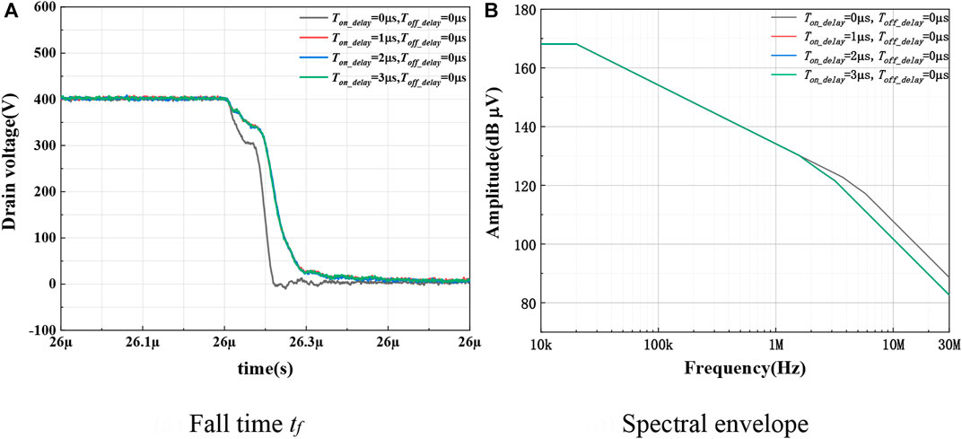
FIGURE 7. Waveforms of CM voltage and its spectral envelope at different Ton_delay (pattern 1). (A) Fall time tf and (B) spectral envelope.
The test results of CM EMI at different Ton_delay (from 0us to 3us) are shown in Figure 8. As can be seen from Figure 8, when Ton_delay is increased from 0us to 1us, the CM EMI noise in the frequency range of 6–8 MHz will be reduced by 0∼2 dB, and the CM EMI noise in the frequency range of 12–30 MHz will be reduced by 0∼8 dB. This means that the influence of the CM EMI noise caused by the Si/SiC hybrid switch will be gradually decreased. However, when Ton_delay is increased from 1us to 3us, the CM EMI noise is almost unchanged. This also means that when Ton_delay is close to 1us, the turn-on characteristic of the Si/SiC hybrid switch has little changed.
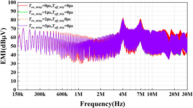
FIGURE 8. Test results of CM EMI at different Ton_delay (pattern 1).
According to Figures 7, 8, the influence of Ton_delay on the EMI noise is limited, because the turn-on speed of the Si/SiC hybrid switch will change little with the increase in Ton_delay.
3.2 Experimental Results of Pattern 2 (Ton_delay and Toff_delay are Changed Simultaneously)
In this condition, when Ton_delay and Toff_delay are changed from 0us to 3us, the waveforms of the CM voltage and its spectral envelope at different Toff_delay are shown in Figure 9. As can be seen from Figures 9A,B, the turn-on characteristic of the Si/SiC hybrid switch reflects the turn-on characteristic of the SiC MOSFET when Ton_delay is set as 0us, and its turn-off characteristic reflects the turn-off characteristic of the Si IGBT when Toff_delay is set as 0us. When Ton_delay and Toff_delay are increased from 0us to 2us, the rise time of the CM voltage will be increased, and the fall time of the CM voltage will be decreased. The spectral envelope in the frequency range of 1–8 MHz will be increased by 0∼3 dB, and the spectral envelope in the frequency range of 8–30 MHz will be decreased by 0∼1 dB. When Ton_delay and Toff_delay are increased from 2us to 3us, the variation of the spectral envelope is small (smaller than 1 dB).
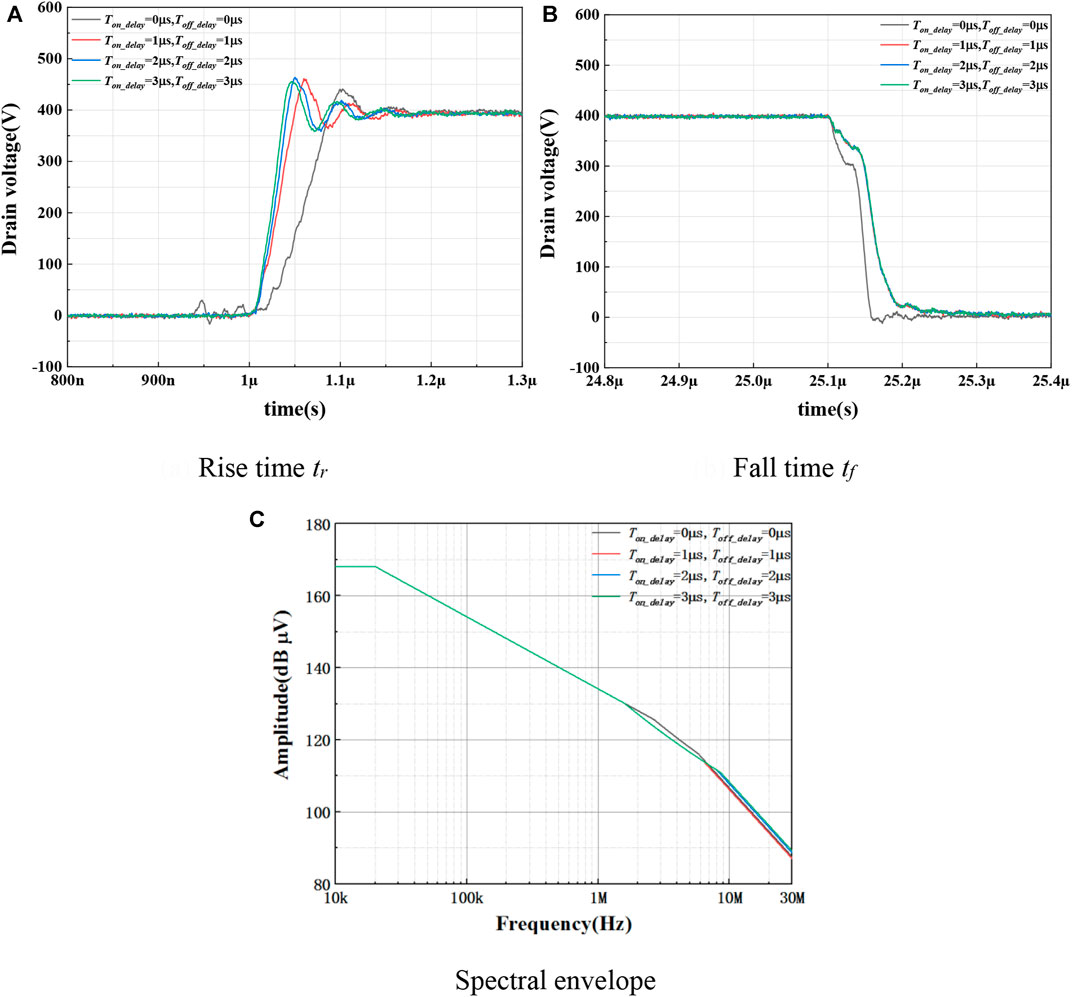
FIGURE 9. Waveforms of CM voltage and its spectral envelope at different Ton_delay and Toff_delay (pattern 2). (A) Rise time tr, (B) fall time tf, and (C) spectral envelope.
The test results of CM EMI at different Ton_delay and Toff_delay are shown in Figure 10. As can be seen from Figure 10, when Ton_delay and Toff_delay are increased from 0us to 2us, the CM EMI noise in the frequency range of 1–4 MHz will be increased by 1∼9 dB, the CM EMI noise in the frequency range of 7–18 MHz will be increased by 1∼5 dB, and the CM EMI noise in the frequency range of 19–30 MHz will be reduced by 1∼7 dB. This means that the influence of the CM EMI noise will be gradually decreased. When Ton_delay and Toff_delay are increased from 1us to 2us, the difference of the CM EMI noise is small (smaller than 1dB). This means that when Ton_delay and Toff_delay are increased from 1us to 2us, the turn-on and turn-off characteristic of the Si/SiC hybrid switch has little changed.
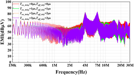
FIGURE 10. Test results of CM EMI at different Ton_delay and Toff_delay (pattern 2).
3.3 Experimental Results of Pattern 4 (Only Toff_delay is Changed)
In this condition, when Toff_delay is changed from 0us to 3us and Ton_delay is set as 0us, the waveforms of the CM voltage and its spectral envelope at different Toff_delay are shown in Figure 11. As can be seen from Figure 11A, when Ton_delay and Toff_delay are set as 0us, the turn-on characteristic of the Si/SiC hybrid switch reflects the turn-on characteristic of the SiC MOSFET, and its turn-off characteristic reflects the turn-off characteristic of the Si IGBT. When Toff_delay is increased from 0us to 2us, the rise time of the CM voltage will be decreased, and the spectral envelope in the frequency range of 4–30 MHz will be increased by 6dB, which is shown in Figure 11B. When Toff_delay is increased from 2us to 3us, the spectral envelope is slightly changed (smaller than 1dB).
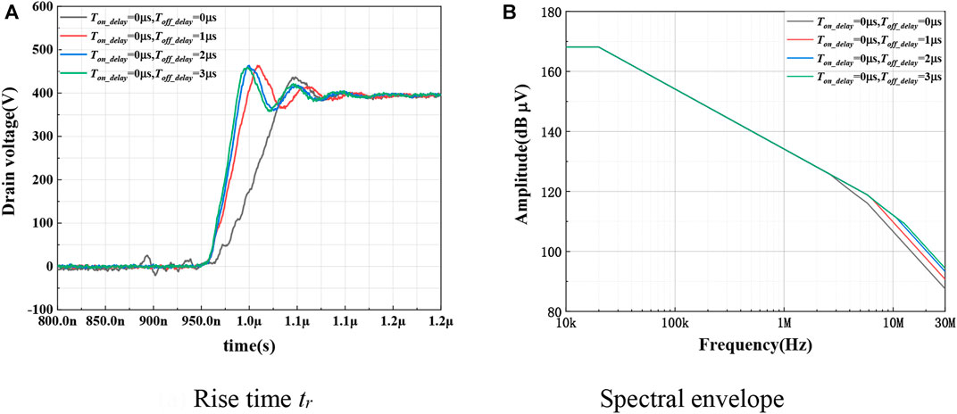
FIGURE 11. Waveforms of CM voltage and its spectral envelope at different Toff_delay (pattern 4). (A) Rise time tr and (B) spectral envelope.
The test results of CM EMI at different Toff_delay (from 0us to 3us) are shown in Figure 12. As can be seen from Figure 12, when Toff_delay is increased from 0us to 1us, the CM EMI noise in the frequency range of 5–8 MHz will be increased by 1∼3 dB, and the CM EMI noise in the frequency range of 23–26 MHz will be increased by 1∼5 dB. Therefore, the influence of the CM EMI noise will be gradually increased. When Toff_delay is increased from 1us to 3us, the CM EMI noise is slightly changed (smaller than 1dB). This means that when Toff_delay is increased from 1us to 3us, the turn-off characteristic of the Si/SiC hybrid switch has little changed.
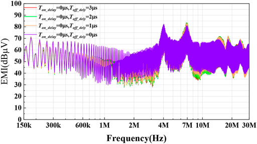
FIGURE 12. Test results of CM EMI at different Toff_delay (pattern 4).
3.4 Different Gate Resistors
The relationship between the gate resistor inside the Si/SiC hybrid switch-based boost converter and the CM EMI noise and power losses is shown in the following.
3.4.1 All gate resistors are changed simultaneously
As can be seen from Figure 13 and Table 2, when all gate resistors increase simultaneously, the generated CM EMI noise will be decreased, but the switching loss of the Si/SiC hybrid switch will be increased, resulting in an increasing loss of the boost converter.
1) Figure 13A shows the CM EMI test results for different gate resistors in pattern 1. When all gate resistors are increased from 5 to 10Ω, the CM EMI noise in the frequency range from 1 to 7 MHz will be reduced by 1∼6 dB, and in the frequency range from 8 to 30 MHz, it will be reduced by 2∼13 dB. When all gate resistors are increased from 10 to 20Ω, the overall CM EMI noise generated does not change much. The overall CM EMI noise generated does not change much.
2) Figure 13B shows the CM EMI test results for different gate resistors in pattern 2. When all the gate resistors are increased from 5 to 20Ω, the CM EMI noise will be reduced by 2∼10 dB in the frequency range from 1 to 7 MHz and by 1∼17 dB in the frequency range from 8 to 30 MHz.
3) Figure 13C shows the CM EMI test results for different gate resistors in pattern 3. When all the driving resistors are increased from 5 to 10Ω, the CM EMI noise will be reduced by 1∼9 dB in the frequency range from 1 to 7 MHz and by 2∼12 dB in the frequency range from 8 to 30 MHz.
4) Figure 13D shows the CM EMI test results for different gate resistors in pattern 4. When all the driving resistors are increased from 5 to 20Ω, the CM EMI noise will be reduced by 1∼11 dB in the frequency range from 1 to 7 MHz and by 1∼17 dB in the frequency range from 8 to 30 MHz.
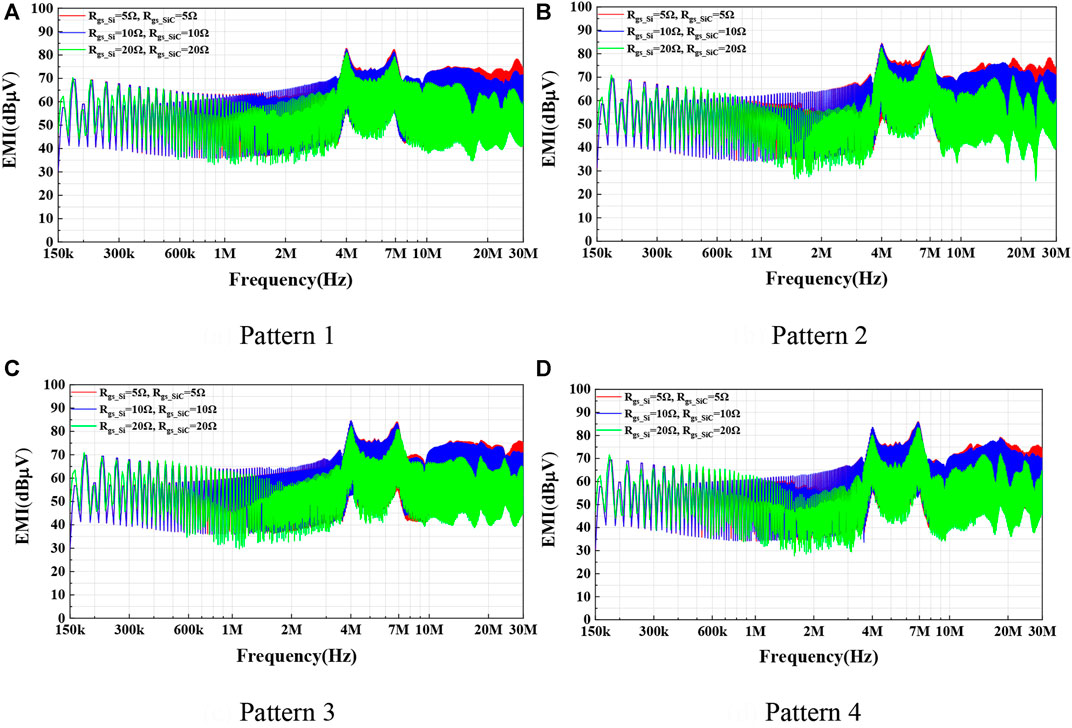
FIGURE 13. Relationship between the gate resistor and CM EMI noise (all gate resistors are changed simultaneously). (A) Pattern 1, (B) pattern 2, (C) pattern 3, and (D) pattern 4.
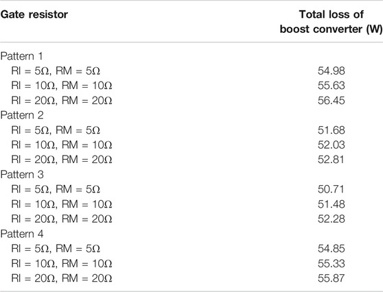
TABLE 2. Relationship between gate resistor and total loss of boost converter (all gate resistors are changed simultaneously).
In fact, the total loss of the boost converter will be increased with the increase in gate resistor.
3.4.2 Gate Resistor of the SiC MOSFET is Changed
When the gate resistor of the SiC MOSFET is changed, the relationship between the Si/SiC hybrid switch-based boost converter and the CM EMI noise and power losses is shown in the following (Figure 14; Table 3).
1) When pattern 1 is taken, the Si/SiC hybrid switch reflects the switching speed of pure Si IGBT, so changing the gate resistor of the SiC MOSFET does not affect the switching characteristics of pattern 1. A comparative study is not conducted here.
2) Figure 14A shows the CM EMI test results of changing the gate resistor of SiC MOSFET in pattern 2. The CM EMI noise decreases by about 0∼5 dB in the frequency range of 1∼30 MHz as the gate resistor of SiC MOSFET is increased.
3) From Figure 14B, when the SiC MOSFET gate resistor is increased in pattern 3, the CM EMI noise is decreased by about 0∼9 dB in the frequency range of 1∼30 MHz.
4) From Figure 14C, the CM EMI noise in pattern 4 decreases by about 0∼7 dB in the frequency range of 1∼30 MHz as the gate resistor of SiC MOSFET is increased.
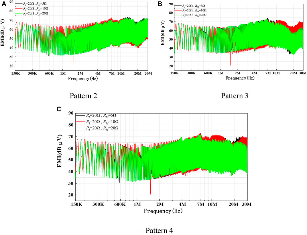
FIGURE 14. Relationship between the gate resistor and CM EMI noise (changing gate resistor of SiC MOSFET). (A) Pattern 2, (B) pattern 3, and (C) pattern 4.
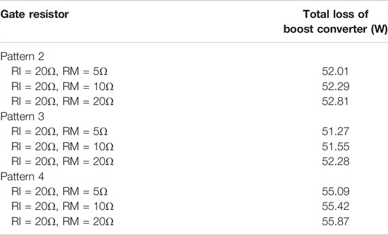
TABLE 3. Relationship between the gate resistor and total loss of boost converter (changing gate resistor of SiC MOSFET).
3.4.3 Gate Resistor of the Si IGBT is Changed
When the gate resistor of the Si IGBT is changed, the relationship between the Si/SiC hybrid switch-based boost converter and the CM EMI noise and power losses is shown in the following (Figure 15; Table 4).
1) When pattern 4 is taken, the Si/SiC hybrid switch reflects the switching speed of the pure SiC MOSFET, so the change of the gate resistor of the Si IGBT does not affect the switching characteristics of pattern 4, which is not studied here for comparison.
2) Figure 15A shows the CM EMI test results of the Si/SiC hybrid switch-based boost converter, when the gate resistor of the Si IGBT in pattern 1 is changed. The CM EMI noise is decreased by about 0∼2 dB in the frequency range of 1∼10 MHz as the gate resistor of Si IGBT is increased.
3) Figure 15B shows the CM EMI test results of changing the gate resistor of the Si IGBT in pattern 2. The CM EMI noise is decreased by about 0∼6 dB in the frequency range of 150kHz∼10 MHz as the gate resistor of the Si IGBT is increased.
4) From Figure 15C, the CM EMI noise in pattern 3 is decreased in the frequency range of 1∼4 MHz and 5∼30 MHz as the Si IGBT gate resistor is increased.
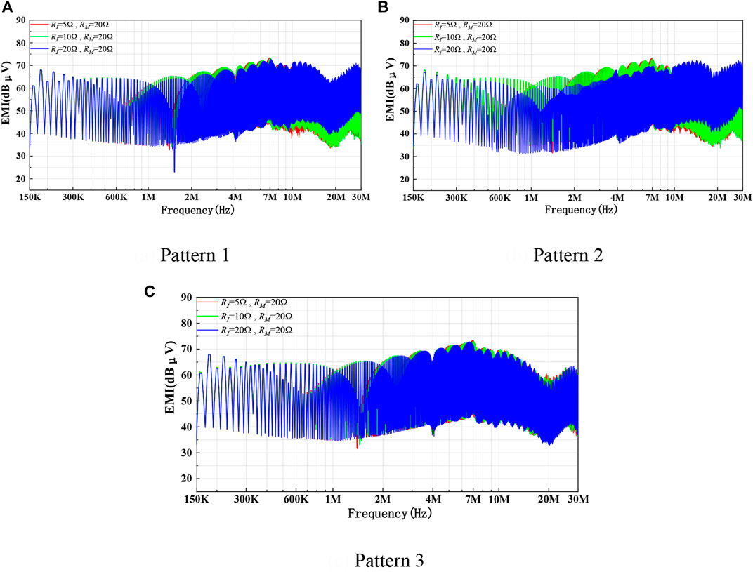
FIGURE 15. Relationship between the gate resistor and CM EMI noise (changing gate resistor of Si IGBT). (A) Pattern 1, (B) pattern 2, and (C) pattern 3.
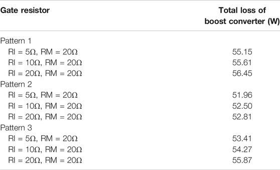
TABLE 4. Relationship between the gate resistor and total loss of boost converter (changing gate resistor of Si IGBT).
In fact, the total loss of the boost converter will be increased with the increase in gate resistor.
3.5 Different Frequencies
The comparison experiments of CM EMI at different switching patterns are shown in Figure 16. Details are shown in the following.
1) As can be seen from Figure 16A, when the switching frequency is set as 20 kHz, the CM EMI noise caused by pattern 4 (Ton_delay and Toff_delay are set as 0us and 2us, respectively) in the frequency range of 3–8 MHz is 0∼5 dB smaller than that of pattern 1 (Ton_delay and Toff_delay are set as 2us and 0us, respectively). In the frequency range of 11–30 MHz, the CM EMI noise caused by pattern 4 is 1∼10 dB smaller than that of pattern 1. The CM EMI noise caused by pattern 4 in the frequency range of 3–8 MHz is 0–5 dB smaller than that of pattern 2 (Ton_delay and Toff_delay are set as 2us and 2us, respectively). In the frequency range of 11–30 MHz, the CM EMI noise caused by pattern 4 is 1∼9 dB smaller than that of pattern 2. Meanwhile, the CM EMI noise caused by pattern 4 in the frequency range of 3–8 MHz is 0–3 dB smaller than that of pattern 3 (Ton_delay and Toff_delay are set as 0us and 0us, respectively). In addition, in the frequency range of 11–30 MHz, the CM EMI noise caused by pattern 4 is 1∼7 dB smaller than that of pattern 3.
2) A scan be seen from Figures 16B,C, as the switching frequency increases, the differences in the CM EMI noise caused by different switching patterns are similar.
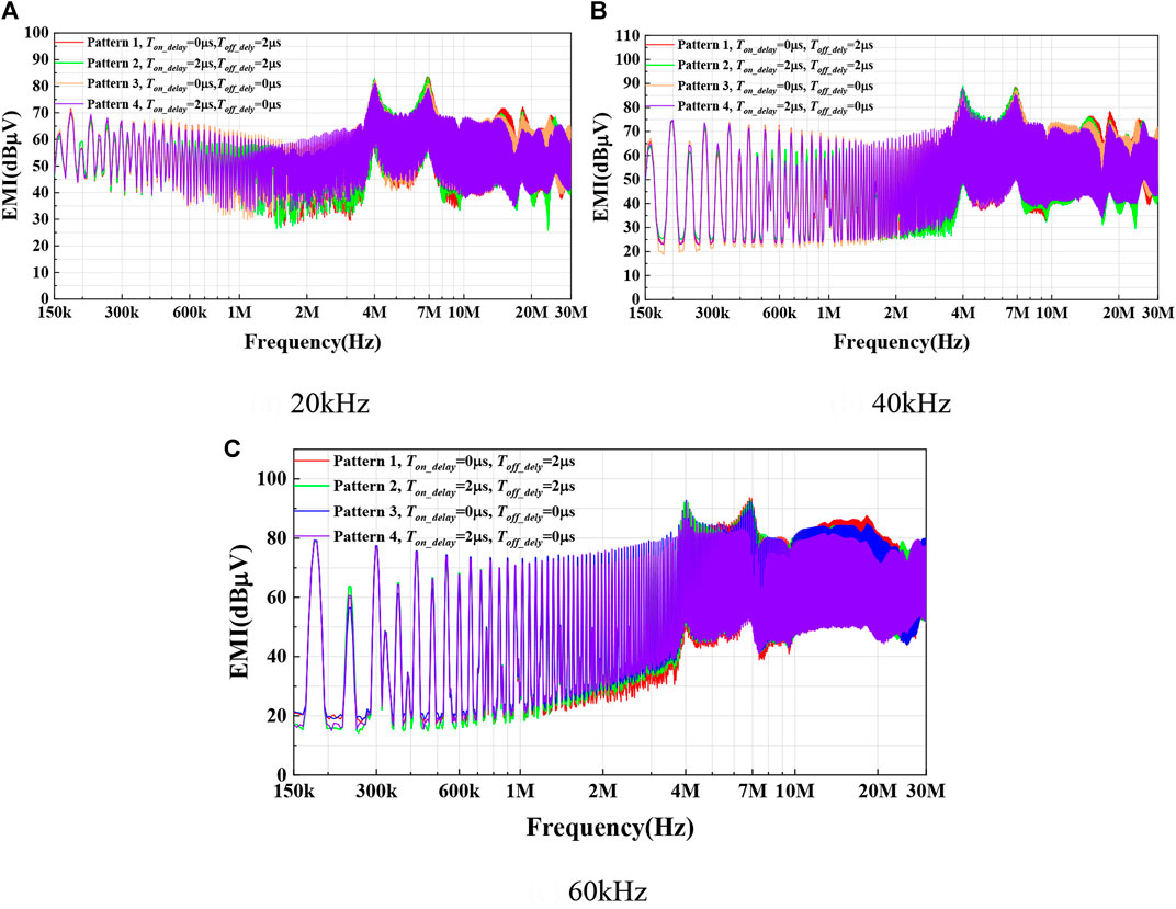
FIGURE 16. Comparisons of different frequencies. (A) 20kHz, (B) 40kHz, and (C) 60kHz.
4 Discussion
According to the above experiments, the following conclusions can be drawn.
1) For different switching patterns, when the delay time increases to the point where the switching characteristic of the Si/SiC hybrid switch does not change, a further increase in the delay time will not cause a significant change in CM EMI noise.
2) The CM EMI noise caused by pattern 4 is worse than that of pattern 1, pattern 2, and pattern 3. The CM EMI noise caused by pattern 1 is better than that of pattern 2 and pattern 3. Furthermore, the CM EMI noise caused by pattern 3 is slightly better than that of pattern 2.
3) Different driving patterns reflect different switching characteristics, the hybrid switch uses different driving resistors in different driving modes, and the resulting CM EMI noise and losses are different. With the gradual increase in gate resistor, the switching speed of the hybrid switch will be reduced, resulting in a longer switching time and increased losses in the hybrid switch. At the same time, the lower switching frequency means a smaller dv/dt. The CM EMI noise of the hybrid switch is reduced.
4) In order to ensure a lower loss, pattern 4 should be taken, and Ton_delay and Toff_delay can be set as 0us and 2us, respectively. Based on the choice of switching mode and switching delay time, a large gate resistance is feasible on the premise that the low EMI noise is suppressed.
5 Conclusion
In this paper, the spectral characteristics of the CM voltage of the Si/SiC hybrid switch at different switching patterns and gate resistors are analyzed to predict the variation of the CM EMI noise. Then, the experimental platform of the Si/SiC hybrid switch-based boost converter is established to verify the correctness of the theory analysis.
The experimental results demonstrate that when the switching delay time exceeds 2us, the EMI noise characteristics have little changed. Moreover, an increase in the gate resistor will result in effective suppression of the EMI noise. Meanwhile, a slower switching speed results in lower CM EMI noise and the rise time has a greater impact on CM EMI than the fall time. The effect of different switching patterns on the CM EMI noise and loss of the Si/SiC hybrid switch is greater than the effect of different gate resistors; although taking the appropriate drive pattern will reduce the switch loss by an order of magnitude, the severe EMI noise generated in this mode is unacceptable.
Pattern 4 is the best choice when the switching mode of the Si/SiC hybrid switch cannot be changed with low loss being a priority. Moreover, Ton_delay can be set as 0. If the switching mode of the Si/SiC hybrid switch can be changed, pattern 1 (low current level) and pattern 4 (high current level) can be considered at different current levels. In fact, the research contents will also be applicable to other types of Si/SiC hybrid switch-based converters.
Data Availability Statement
The original contributions presented in the study are included in the article/Supplementary Material, further inquiries can be directed to the corresponding authors.
Author Contributions
All authors listed have made a substantial, direct, and intellectual contribution to the work and approved it for publication.
Funding
Project supported by State Key Laboratory of Power System and Generation Equipment (SKLD21KM05), Hunan Provincial Natural Science Foundation of China (Grant No. 2019JJ60034), and Scientific Research Foundation of Hunan Provincial Department of Education (No. 19A106).
Conflict of Interest
Author YZ was employed by the company Shenzhen Jingquanhua Electronics Co., Ltd.
The remaining authors declare that the research was conducted in the absence of any commercial or financial relationships that could be construed as a potential conflict of interest.
Publisher’s Note
All claims expressed in this article are solely those of the authors and do not necessarily represent those of their affiliated organizations, or those of the publisher, the editors and the reviewers. Any product that may be evaluated in this article, or claim that may be made by its manufacturer, is not guaranteed or endorsed by the publisher.
References
Cui, T., Ma, Q., Xu, P., and Wang, Y. (2017). Analysis and Optimization of Power MOSFETs Shaped Switching Transients for Reduced EMI Generation. IEEE Access 5, 20440–20448. doi:10.1109/access.2017.2758443
Deshpande, A., and Luo, F. (2019). Practical Design Considerations for a Si IGBT + SiC MOSFET Hybrid Switch: Parasitic Interconnect Influences, Cost, and Current Ratio Optimization. IEEE Trans. Power Electron. 34 (1), 724–737. doi:10.1109/tpel.2018.2827989
Domurat-Linde, A., Dieter Lang, K., and Hoene, E. (2012). “Influence of IGBT-Module Switching Characteristics to Radio Frequency Noise,” in International Symposium on Electromagnetic Compatibility - EMC EUROPE, 1–6. doi:10.1109/emceurope.2012.6396769
Du, M.-X., Bian, W., Wang, H., Dai, Q., and Ouyang, Z. (2021). Research on Conducted Emi Characteristics of Sic Mosfet Considering Temperature Effect. Pier C 112, 69–82. doi:10.2528/pierc21030303
Fang, Z., Jiang, D., and Zhang, Y. (2018). Study of the Characteristics and Suppression of EMI of Inverter with SiC and Si Devices. Chin. J. Electr. Eng. 4 (3), 37–46. doi:10.23919/CJEE.2018.8471288
Gong, X., Ferreira, J. A., and Popovic-Gerber, J. (2012). “Comparison and Suppression of CM EMI in SiC JFET and Si IGBT Based Motor Drives,” in 2012 15th International Power Electronics and Motion Control Conference (EPE/PEMC), DS2c.8-1–DS2c.8-8.
Han, D., Li, S., Wu, Y., Choi, W., and Sarlioglu, B. (2017a). Comparative Analysis on Conducted CM EMI Emission of Motor Drives: WBG versus Si Devices. IEEE Trans. Ind. Electron. 64 (10), 8353–8363. doi:10.1109/tie.2017.2681968
Han, D., Li, S., Wu, Y., Choi, W., and Sarlioglu, B. (2017b). Comparative analysis on conducted cm emi emission of motor drives: Wbg versus si devices. IEEE Trans. Ind. Electron. 64 (10), 8353–8363. doi:10.1109/tie.2017.2681968
He, J., Katebi, R., and Weise, N. (2017). A Current-dependent Switching Strategy for Si/SiC Hybrid Switch-Based Power Converters. IEEE Trans. Ind. Electron. 64 (10), 8344–8352. doi:10.1109/tie.2017.2708033
He, Z., Li, Z., Yuan, F., Zeng, C., Jiang, X., and Wang, J. (2018). “Active Thermal Control of SiC/Si Hybrid Switch,” in 2018 IEEE International Power Electronics and Application Conference and Exposition (PEAC), 1–4. doi:10.1109/peac.2018.8590287
Huang, A. Q., Song, X., and Zhang, L. (2015). “6.5 kV Si/SiC Hybrid Power Module: An Ideal Next Step,” in 2015 IEEE International Workshop on Integrated Power Packaging (IWIPP), 64–67.
Igarashi, S., Takubo, H., Kobayashi, Y., Otsuki, M., and Miyasaka, T. (2007). “Low EMI Noise Techniques of the 6th Generation IGBT Module,” in 2007 European Conference on Power Electronics and Applications, 1–8.
Infineon (2019). [Online] Available: http://www.infineon.com.
Ji, Q., Ruan, X., and Ye, Z. (2015). The Worst Conducted EMI Spectrum of Critical Conduction Mode Boost PFC Converter. IEEE Trans. Power Electron. 30 (3), 1230–1241. doi:10.1109/tpel.2014.2317172
Jiang, Y., Hua, G. C., Yang, E., and Lee, F. C. (1993). Soft-switching of IGBTs with the Help of MOSFETs in Bridge-type Converters. Proc. IEEE Power Electron. Specialist Conf. - PESC 93, 151–157.
Kim, T., Feng, D., Jang, M., and Agelidis, V. G. (2017). Common Mode Noise Analysis for Cascaded Boost Converter with Silicon Carbide Devices. IEEE Trans. Power Electron. 32 (3), 1917–1926. doi:10.1109/tpel.2016.2569424
Li, L., Ning, P., Wen, P. X., and Zhang, D. (2018). A 1200 V/200 a Half-Bridge Power Module Based on Si IGBT/SiC MOSFET Hybrid Switch. Cpss Tpea 3 (4), 292–300. doi:10.24295/cpsstpea.2018.00029
Li, L., Ning, P., Wen, X., Bian, Y., and Zhang, D. (2018). “Gate Drive Design for a Hybrid Si IGBT/SiC MOSFET Module,” in 2018 1st Workshop on Wide Bandgap Power Devices and Applications in Asia (WiPDA Asia), 34–41.
Li, Z., Jiang, X., Zeng, C., He, Z., and Wang, J. (2018). “Gate Control Optimization of Si/SiC Hybrid Switch within Wide Power Rating Range,” in 2018 1st Workshop on Wide Bandgap Power Devices and Applications in Asia (WiPDA Asia), 265–269. doi:10.1109/wipdaasia.2018.8734625
Li, L., Ning, P., Wen, X., Ge, Q., and Li, Y. (2019). “A 30kW Three-phase Voltage Source Inverter Based on the Si IGBT/SiC MOSFET Hybrid Switch,” in 2019 IEEE Applied Power Electronics Conference and Exposition (APEC), 1397–1401.
Liu, Z., Peng, Z., Peng, X., and Wang, J. (2019). “Current-dependent Variable Switching Strategy for Si/SiC Hybrid Switch Based Single-phase Inverter,” in 2019 IEEE Energy Conversion Congress and Exposition (ECCE), 1922–1925.
Minamisawa, R. A., Vemulapati, U., Mihaila, A., Papadopoulos, C., and Rahimo, M. (2016). Current Sharing Behavior in Si IGBT and SiC MOSFET Cross-Switch Hybrid. IEEE Electron. Device Lett. 37 (9), 1178–1180. doi:10.1109/led.2016.2596302
Oswald, N., Anthony, P., McNeill, N., and Stark, B. H. (2014). An Experimental Investigation of the Tradeoff between Switching Losses and EMI Generation with Hard-Switched All-Si, Si-SiC, and All-SiC Device Combinations. IEEE Trans. Power Electron. 29 (5), 2393–2407. doi:10.1109/tpel.2013.2278919
Oswald, N., Stark, B. H., Holliday, D., Hargis, C., and Drury, B. (2011). Analysis of Shaped Pulse Transitions in Power Electronic Switching Waveforms for Reduced EMI Generation. IEEE Trans. Ind. Applicat. 47 (5), 2154–2165. doi:10.1109/tia.2011.2161971
Peng, Z., Wang, J., Liu, Z., Dai, Y., Zeng, G., and Shen, Z. J. (2020). Fault-Tolerant Inverter Operation Based on Si/SiC Hybrid Switches. IEEE J. Emerg. Sel. Top. Power Electron. 8 (1), 545–556. doi:10.1109/jestpe.2019.2952170
Qi, T., Graham, J., and Sun, J. (2010). “Characterization of IGBT Modules for System EMI Simulation,” in 2010 Twenty-Fifth Annual IEEE Applied Power Electronics Conference and Exposition (APEC), 2220–2225. doi:10.1109/apec.2010.5433545
Rahimo, M., Canales, F., Minamisawa, R. A., Papadopoulos, C., Vemulapati, U., Mihaila, A., et al. (2015). Characterization of a Silicon IGBT and Silicon Carbide MOSFET Cross-Switch Hybrid. IEEE Trans. Power Electron. 30 (9), 4638–4642. doi:10.1109/tpel.2015.2402595
Rohm (2019). [Online] Available: https://www.rohm.com.
Roscoe, N. M., Zhong, Y., and Finney, S. J. (2015). “Comparing SiC MOSFET, IGBT and Si MOSFET in LV Distribution Inverters,” in IECON 2015 - 41st Annual Conference of the IEEE Industrial Electronics Society, 000743–000748. doi:10.1109/iecon.2015.7392188
Song, X., and Huang, A. Q. (2015). “6.5kV FREEDM-Pair: Ideal High Power Switch Capitalizing on Si and SiC,” in 2015 17th European Conference on Power Electronics and Applications (EPE'15 ECCE-Europe), 1–9. doi:10.1109/epe.2015.7309243
Ueno, S., Kimura, N., Morizane, T., and Omori, H. (2017). “Study on Characteristics of Hybrid Switch Using Si IGBT and SiC MOSFET Depending on External Parameters,” in 2017 19th European Conference on Power Electronics and Applications (EPE'17 ECCE Europe), P.1–P.10. doi:10.23919/epe17ecceeurope.2017.8099142
Zhang, H., Yang, L., Wang, S., and Puukko, J. (2017). Common-Mode EMI Noise Modeling and Reduction with Balance Technique for Three-Level Neutral Point Clamped Topology. IEEE Trans. Ind. Electron. 64 (9), 7563–7573. doi:10.1109/tie.2017.2677344
Keywords: hybrid switch, gate drive patterns, gate resistors, CM EMI, reliability
Citation: Zhu Y, Peng Z, Dai Y, Zhao Z, Liu Z and Zheng Z (2022) Study on the CM EMI Generation Characteristics of the Si/SiC Hybrid Switch at Different Switching Patterns and Gate Resistors. Front. Electron. 2:789902. doi: 10.3389/felec.2021.789902
Received: 05 October 2021; Accepted: 27 December 2021;
Published: 21 March 2022.
Edited by:
Kun Xu, Shenzhen Institutes of Advanced Technology (CAS), ChinaCopyright © 2022 Zhu, Peng, Dai, Zhao, Liu and Zheng. This is an open-access article distributed under the terms of the Creative Commons Attribution License (CC BY). The use, distribution or reproduction in other forums is permitted, provided the original author(s) and the copyright owner(s) are credited and that the original publication in this journal is cited, in accordance with accepted academic practice. No use, distribution or reproduction is permitted which does not comply with these terms.
*Correspondence: Yuxing Dai, daiyx@hnu.edu.cn; Zhenxing Zhao, 22006@hnie.edu.cn