
 E-mail Alert
 RSS
RSS
| Citation: |
Yang X, Lin Y, Wu TZ, Yan ZJ, Chen Z et al. An overview on the principle of inkjet printing technique and its application in micro-display for augmented/virtual realities. Opto-Electron Adv 5, 210123 (2022). doi: 10.29026/oea.2022.210123

|
An overview on the principle of inkjet printing technique and its application in micro-display for augmented/virtual realities
-
Abstract
Augmented reality (AR) and virtual reality (VR) are two novel display technologies that are under updates. The essential feature of AR/VR is the full-color display that requires high pixel densities. To generate three-color pixels, the fluorescent color conversion layer inevitably includes green and red pixels. To fabricate such sort of display kits, inkjet printing is a promising way to position the color conversion layers. In this review article, the progress of AR/VR technologies is first reviewed, and in succession, the state of the art of inkjet printing, as well as two key issues — the optimization of ink and the reduction of coffee-ring effects, are introduced. Finally, some potential problems associated with the color converting layer are highlighted.-
Keywords:
- micro-LED /
- quantum dots /
- augmented reality /
- virtual reality /
- inkjet printing
-

-
References
[1] Soohoo S, Torchia M, Srivastava R, Cong M, Dimitrov L et al. IDC’s worldwide augmented reality and virtual reality spending guide taxonomy, 2020: release V2.https://www.idc.com/getdoc.jsp?containerId=US47062820. [2] Liu ZJ, Lin CH, Hyun BR, Sher CW, Lv ZJ et al. Micro-light-emitting diodes with quantum dots in display technology. Light:Sci Appl 9, 83 (2020). doi: 10.1038/s41377-020-0268-1 [3] Joo WJ, Kyoung J, Esfandyarpour M, Lee SH, Koo H et al. Metasurface-driven OLED displays beyond 10, 000 pixels per inch. Science 370, 459–463 (2020). doi: 10.1126/science.abc8530 [4] Gou FW, Chen HW, Li MC, Lee SL, Wu ST. Motion-blur-free LCD for high-resolution virtual reality displays. J Soc Inf Dis 26, 223–228 (2018). doi: 10.1002/jsid.662 [5] Huang Y, Liao E, Chen R, Wu ST. Liquid-crystal-on-silicon for augmented reality displays. Appl Sci 8, 2366 (2018). doi: 10.3390/app8122366 [6] Lee JH, Cheng IC, Hua H, Wu ST. Introduction to Flat Panel Displays 2nd ed (John Wiley & Sons, Hoboken, 2020). [7] Qi LH, Zhang X, Chong WC, Li PA, Lau KM. 848 PPI high-brightness active-matrix micro-LED micro-display using GaN-on-Si epi-wafers towards mass production. Opt Express 29, 10580–10591 (2021). doi: 10.1364/OE.419877 [8] Wu YF, Ma JS, Su P, Zhang LJ, Xia BZ. Full-color realization of micro-LED displays. Nanomaterials 10, 2482 (2020). doi: 10.3390/nano10122482 [9] Kwak BC, Kwon OK. A 2822-ppi resolution pixel circuit with high luminance uniformity for OLED microdisplays. J Dis Technol 12, 1083–1088 (2016). doi: 10.1109/JDT.2016.2593048 [10] Motoyama Y, Sugiyama K, Tanaka H, Tsuchioka H, Matsusaki K et al. High-efficiency OLED microdisplay with microlens array. J Soc Inf Dis 27, 354–360 (2019). doi: 10.1002/jsid.784 [11] Vieri C, Lee G, Balram N, Jung SH, Yang JY et al. An 18 megapixel 4.3" 1443 ppi 120 Hz OLED display for wide field of view high acuity head mounted displays. J Soc Inf Dis 26, 314–324 (2018). doi: 10.1002/jsid.658 [12] Moverio BT-40 smart glasses with USB type-C connectivity.https://epson.com/For-Work/Wearables/Smart-Glasses/Moverio-BT-40-Smart-Glasses-with-USB-Type-C-Connectivity-/p/V11H969020. [13] Wu TZ, Sher CW, Lin Y, Lee CF, Liang SJ et al. Mini-LED and micro-LED: promising candidates for the next generation display technology. Appl Sci 8, 1557 (2018). doi: 10.3390/app8091557 [14] Lin JY, Jiang HX. Development of microLED. Appl Phys Lett 116, 100502 (2020). doi: 10.1063/1.5145201 [15] Chen SWH, Shen CC, Wu TZ, Liao ZY, Chen LF et al. Full-color monolithic hybrid quantum dot nanoring micro light-emitting diodes with improved efficiency using atomic layer deposition and nonradiative resonant energy transfer. Photonics Res 7, 416–422 (2019). doi: 10.1364/PRJ.7.000416 [16] Han HV, Lin HY, Lin CC, Chong WC, Li JR et al. Resonant-enhanced full-color emission of quantum-dot-based micro LED display technology. Opt Express 23, 32504–32515 (2015). doi: 10.1364/OE.23.032504 [17] Jiang CB, Zhong ZM, Liu BQ, He ZW, Zou JH et al. Coffee-ring-free quantum dot thin film using inkjet printing from a mixed-solvent system on modified ZnO transport layer for light-emitting devices. ACS Appl Mater Interfaces 8, 26162–26168 (2016). doi: 10.1021/acsami.6b08679 [18] Shi SC, Bai WH, Xuan TT, Zhou TL, Dong GY et al. In situ inkjet printing patterned lead halide perovskite quantum dot color conversion films by using cheap and eco-friendly aqueous inks. Small Methods 5, 2000889 (2021). doi: 10.1002/smtd.202000889 [19] Zhu MH, Duan YQ, Liu N, Li HG, Li JH et al. Electrohydrodynamically printed high-resolution full-color hybrid perovskites. Adv Funct Mater 29, 1903294 (2019). doi: 10.1002/adfm.201903294 [20] Wilkinson NJ, Smith MAA, Kay RW, Harris RA. A review of aerosol jet printing—a non-traditional hybrid process for micro-manufacturing. Int J Adv Manuf Technol 105, 4599–4619 (2019). doi: 10.1007/s00170-019-03438-2 [21] Chen G, Gu Y, Tsang H, Hines DR, Das S. The effect of droplet sizes on overspray in aerosol-jet printing. Adv Eng Mater 20, 1701084 (2018). doi: 10.1002/adem.201701084 [22] Onses MS, Sutanto E, Ferreira PM, Alleyne AG, Rogers JA. Mechanisms, capabilities, and applications of high-resolution electrohydrodynamic jet printing. Small 11, 4237–4266 (2015). doi: 10.1002/smll.201500593 [23] Huang QJ, Zhu Y. Printing conductive nanomaterials for flexible and stretchable electronics: a review of materials, processes, and applications. Adv Mater Technol 4, 1800546 (2019). doi: 10.1002/admt.201800546 [24] Laurila MM. Super inkjet Printed redistribution layer for a MEMS device (Tampere University of Technology, Tampere, 2015). [25] Jin SX, Li J, Li JZ, Lin JY, Jiang HX. GaN microdisk light emitting diodes. Appl Phys Lett 76, 631–633 (2000). doi: 10.1063/1.125841 [26] Liu ZJ, Zhang K, Liu YB, Yan SW, Kwok HS et al. Fully multi-functional GaN-based micro-LEDs for 2500 PPI micro-displays, temperature sensing, light energy harvesting, and light detection. 2018 IEEE International Electron Devices Meeting (IEDM) 38.1. 1–38.1. 4 (IEEE, 2018);http://doi.org/10.1109/IEDM.2018.8614692. [27] Zhang L, Ou F, Chong WC, Chen YJ, Li QM. Wafer-scale monolithic hybrid integration of Si-based IC and III-V epi-layers—A mass manufacturable approach for active matrix micro-LED micro-displays. J Soc Inf Dis 26, 137–145 (2018). doi: 10.1002/jsid.649 [28] Seong J, Jang J, Lee J, Lee M. CMOS backplane pixel circuit with leakage and voltage drop compensation for an micro-LED display achieving 5000 PPI or higher. IEEE Access 8, 49467–49476 (2020). doi: 10.1109/ACCESS.2020.2979883 [29] Park J, Choi JH, Kong K, Han JH, Park JH et al. Electrically driven mid-submicrometre pixelation of InGaN micro-light-emitting diode displays for augmented-reality glasses. Nat Photonics 15, 449–455 (2021). doi: 10.1038/s41566-021-00783-1 [30] Lee YH, Zhan T, Wu ST. Prospects and challenges in augmented reality displays. Virtual Real Intell Hardw 1, 10–20 (2019). doi: 10.3724/SP.J.2096-5796.2018.0009 [31] Achermann M, Petruska MA, Kos S, Smith DL, Koleske DD et al. Energy-transfer pumping of semiconductor nanocrystals using an epitaxial quantum well. Nature 429, 642–646 (2004). doi: 10.1038/nature02571 [32] Fan XT, Wu TZ, Liu B, Zhang R, Kuo HC et al. Recent developments of quantum dot based micro-LED based on non-radiative energy transfer mechanism. Opto-Electron Adv 4, 210022 (2021). [33] Zhuang Z, Guo X, Liu B, Hu FR, Li Y et al. High color rendering index hybrid III-nitride/nanocrystals white light-emitting diodes. Adv Funct Mater 26, 36–43 (2016). doi: 10.1002/adfm.201502870 [34] Zhao JL, Bardecker JA, Munro AM, Liu MS, Niu YH et al. Efficient CdSe/CdS quantum dot light-emitting diodes using a thermally polymerized hole transport layer. Nano Lett 6, 463–467 (2006). doi: 10.1021/nl052417e [35] Prins F, Sumitro A, Weidman MC, Tisdale WA. Spatially resolved energy transfer in patterned colloidal quantum dot heterostructures. ACS Appl Mater Interfaces 6, 3111–3114 (2014). doi: 10.1021/am500197n [36] Cadusch JJ, Panchenko E, Kirkwood N, James TD, Gibson BC et al. Emission enhancement and polarization of semiconductor quantum dots with nanoimprinted plasmonic cavities: towards scalable fabrication of plasmon-exciton displays. Nanoscale 7, 13816–13821 (2015). doi: 10.1039/C5NR04042F [37] Lin SY, Tan GJ, Yu JH, Chen EG, Weng YL et al. Multi-primary-color quantum-dot down-converting films for display applications. Opt Express 27, 28480–28493 (2019). doi: 10.1364/OE.27.028480 [38] Liu Y, Han F, Li FS, Zhao Y, Chen MS et al. Inkjet-printed unclonable quantum dot fluorescent anti-counterfeiting labels with artificial intelligence authentication. Nat Commun 10, 2409 (2019). doi: 10.1038/s41467-019-10406-7 [39] Bao B, Jiang JK, Li FY, Zhang PC, Chen SR et al. Fabrication of patterned concave microstructures by inkjet imprinting. Adv Funct Mater 25, 3286–3294 (2015). doi: 10.1002/adfm.201500908 [40] Bao B, Li MZ, Li Y, Jiang JK, Gu ZK et al. Patterning fluorescent quantum dot nanocomposites by reactive inkjet printing. Small 11, 1649–1654 (2015). doi: 10.1002/smll.201403005 [41] Lin HY, Sher CW, Hsieh DH, Chen XY, Chen HMP et al. Optical cross-talk reduction in a quantum-dot-based full-color micro-light-emitting-diode display by a lithographic-fabricated photoresist mold. Photonics Res 5, 411–416 (2017). doi: 10.1364/PRJ.5.000411 [42] Ho SJ, Hsu HC, Yeh CW, Chen HS. Inkjet-printed salt-encapsulated quantum dot film for UV-based RGB color-converted micro-light emitting diode displays. ACS Appl Mater Interfaces 12, 33346–33351 (2020). doi: 10.1021/acsami.0c05646 [43] Duan M, Feng ZY, Wu YW, Yin YM, Hu ZP et al. Inkjet-printed micrometer-thick patterned perovskite quantum dot films for efficient blue-to-green photoconversion. Adv Mater Technol 4, 1900779 (2019). doi: 10.1002/admt.201900779 [44] Lee SY, Lee G, Kim DY, Jang SH, Choi I et al. Investigation of high-performance perovskite nanocrystals for inkjet-printed color conversion layers with superior color purity. APL Photonics 6, 056104 (2021). doi: 10.1063/5.0044284 [45] Yin YM, Hu ZP, Ali MU, Duan M, Gao L et al. Full-color micro-LED display with CsPbBr3 perovskite and CdSe quantum dots as color conversion layers. Adv Mater Technol 5, 2000251 (2020). doi: 10.1002/admt.202000251 [46] Hu ZP, Yin YM, Ali MU, Peng WX, Zhang SJ et al. Inkjet printed uniform quantum dots as color conversion layers for full-color OLED displays. Nanoscale 12, 2103–2110 (2020). doi: 10.1039/C9NR09086J [47] Mathies F, List-Kratochvil EJW, Unger EL. Advances in inkjet-printed metal halide perovskite photovoltaic and optoelectronic devices. Energy Technol 8, 1900991 (2020). doi: 10.1002/ente.201900991 [48] Liu R, Ding HY, Lin J, Shen FP, Cui Z et al. Fabrication of platinum-decorated single-walled carbon nanotube based hydrogen sensors by aerosol jet printing. Nanotechnology 23, 505301 (2012). doi: 10.1088/0957-4484/23/50/505301 [49] Tsuji H, Nakata M, Nakajima Y, Takei T, Fujisaki Y et al. Development of back-channel etched In-W-Zn-O thin-film transistors. J Dis Technol 12, 228–231 (2016). doi: 10.1109/JDT.2015.2445321 [50] Murata K, Masuda K. Super inkjet printer technology and its properties. Convertech e-Print 1, 108–111 (2011). [51] Xuan TT, Shi SC, Wang L, Kuo HC, Xie RJ. Inkjet-printed quantum dot color conversion films for high-resolution and full-color micro light-emitting diode displays. J Phys Chem Lett 11, 5184–5191 (2020). doi: 10.1021/acs.jpclett.0c01451 [52] Derby B. Inkjet printing ceramics: from drops to solid. J Eur Ceram Soc 31, 2543–2550 (2011). doi: 10.1016/j.jeurceramsoc.2011.01.016 [53] Meixner RM, Cibis D, Krueger K, Goebel H. Characterization of polymer inks for drop-on-demand printing systems. Microsyst Technol 14, 1137–1142 (2008). doi: 10.1007/s00542-008-0639-7 [54] Jang D, Kim D, Moon J. Influence of fluid physical properties on ink-jet printability. Langmuir 25, 2629–2635 (2009). doi: 10.1021/la900059m [55] Giuri A, Saleh E, Listorti A, Colella S, Rizzo A et al. Rheological tunability of perovskite precursor solutions: from spin coating to inkjet printing process. Nanomaterials 9, 582 (2019). doi: 10.3390/nano9040582 [56] Nallan HC, Sadie JA, Kitsomboonloha R, Volkman SK, Subramanian V. Systematic design of jettable nanoparticle-based inkjet inks: rheology, acoustics, and jettability. Langmuir 30, 13470–13477 (2014). doi: 10.1021/la502903y [57] Chen M, Xie LM, Wei CT, Yi YQQ, Chen XL et al. High performance inkjet-printed QLEDs with 18.3% EQE: improving interfacial contact by novel halogen-free binary solvent system. Nano Res 14, 4125–4131 (2021). doi: 10.1007/s12274-021-3352-9 [58] Roh H, Ko D, Shin DY, Chang JH, Hahm D et al. Enhanced performance of pixelated quantum dot light-emitting diodes by inkjet printing of quantum dot-polymer composites. Adv Opt Mater 9, 2002129 (2021). doi: 10.1002/adom.202002129 [59] Jiang CB, Mu L, Zou JH, He ZW, Zhong ZJ et al. Full-color quantum dots active matrix display fabricated by ink-jet printing. Sci China Chem 60, 1349–1355 (2017). doi: 10.1007/s11426-017-9087-y [60] Yang PH, Zhang L, Kang DJ, Strahl R, Kraus T. High-resolution inkjet printing of quantum dot light-emitting microdiode arrays. Adv Opt Mater 8, 1901429 (2020). doi: 10.1002/adom.201901429 [61] Mathies F, Abzieher T, Hochstuhl A, Glaser K, Colsmann A et al. Multipass inkjet printed planar methylammonium lead iodide perovskite solar cells. J Mater Chem A 4, 19207–19213 (2016). doi: 10.1039/C6TA07972E [62] Gu ZK, Wang K, Li HZ, Gao M, Li LH et al. Direct-writing multifunctional perovskite single crystal arrays by inkjet printing. Small 13, 1603217 (2017). doi: 10.1002/smll.201603217 [63] Li PW, Liang C, Bao B, Li YN, Hu XT et al. Inkjet manipulated homogeneous large size perovskite grains for efficient and large-area perovskite solar cells. Nano Energy 46, 203–211 (2018). doi: 10.1016/j.nanoen.2018.01.049 [64] YousefiAmin A, Killilea NA, Sytnyk M, Maisch P, Tam KC et al. Fully printed infrared photodetectors from PbS nanocrystals with perovskite ligands. ACS Nano 13, 2389–2397 (2019). [65] Wong YC, Wu WB, Wang T, Ng JDA, Khoo KH et al. Color patterning of luminescent perovskites via light-mediated halide exchange with haloalkanes. Adv Mater 31, 1901247 (2019). [66] Choi S, Lee SY, Kim DY, Park HK, Ko MJ et al. The synthesis and characterisation of the highly stable perovskite nano crystals and their application to ink-jet printed colour conversion layers. J Indust Eng Chem 85, 226–239 (2020). doi: 10.1016/j.jiec.2020.02.005 [67] Liu Y, Li FS, Veeramalai CP, Chen W, Guo TL et al. Inkjet-printed photodetector arrays based on hybrid perovskite CH3NH3PbI3 microwires. ACS Appl Mater Interfaces 9, 11662–11668 (2017). doi: 10.1021/acsami.7b01379 [68] Liu Y, Li FS, Qiu LC, Yang KY, Li QQ et al. Fluorescent microarrays of in situ crystallized perovskite nanocomposites fabricated for patterned applications by using inkjet printing. ACS Nano 13, 2042–2049 (2019). [69] Shi LF, Meng LH, Jiang F, Ge Y, Li F et al. In situ inkjet printing strategy for fabricating perovskite quantum dot patterns. Adv Funct Mater 29, 1903648 (2019). doi: 10.1002/adfm.201903648 [70] Zou WH, Yu HB, Zhou PL, Zhong Y, Wang YC et al. High-resolution additive direct writing of metal micro/nanostructures by electrohydrodynamic jet printing. Appl Surf Sci 543, 148800 (2021). doi: 10.1016/j.apsusc.2020.148800 [71] Li HG, Duan YQ, Shao ZL, Zhang GN, Li HY et al. High-resolution pixelated light emitting diodes based on electrohydrodynamic printing and coffee-ring-free quantum dot film. Adv Mater Technol 5, 2000401 (2020). doi: 10.1002/admt.202000401 [72] Cho TH, Farjam N, Allemang CR, Pannier CP, Kazyak E et al. Area-selective atomic layer deposition patterned by electrohydrodynamic jet printing for additive manufacturing of functional materials and devices. ACS Nano 14, 17262–17272 (2020). doi: 10.1021/acsnano.0c07297 [73] Kim BH, Onses MS, Lim JB, Nam S, Oh N et al. High-resolution patterns of quantum dots formed by electrohydrodynamic jet printing for light-emitting diodes. Nano Lett 15, 969–973 (2015). doi: 10.1021/nl503779e [74] Yakunin S, Chaaban J, Benin BM, Cherniukh I, Bernasconi C et al. Radiative lifetime-encoded unicolour security tags using perovskite nanocrystals. Nat Commun 12, 981 (2021). doi: 10.1038/s41467-021-21214-3 [75] Park JU, Hardy M, Kang SJ, Barton K, Adair K et al. High-resolution electrohydrodynamic jet printing. Nat Mater 6, 782–789 (2007). doi: 10.1038/nmat1974 [76] Murata K, Sagisaka H, Shimizu K, Matsuba Y, Yokoyama H. Minimal manufacturing process by using a super fine inkjet system. In 2005 4th International Symposium on Environmentally Conscious Design and Inverse Manufacturing 588–589 (IEEE, 2005); http://doi.org/10.1109/ECODIM.2005.1619302. [77] Shirakawa N, Kajihara K, Kashiwagi Y, Murata K. Fine-pitch copper wiring formed in a platingless process using ultra-fine inkjet and oxygen pump. In 2015 International Conference on Electronics Packaging and iMAPS All Asia Conference (ICEP-IAAC) 373–376 (IEEE, 2015);http://doi.org/10.1109/ICEP-IAAC.2015.7111038. [78] Leppäniemi J, Mattila T, Eiroma K, Miyakawa T, Murata K et al. Printed low-voltage fuse memory on paper. IEEE Electron Device Lett 35, 354–356 (2014). doi: 10.1109/LED.2014.2300413 [79] Zhang J, Geng BW, Duan SM, Huang CC, Xi Y et al. High-resolution organic field-effect transistors manufactured by electrohydrodynamic inkjet printing of doped electrodes. J Mater Chem C 8, 15219–15223 (2020). doi: 10.1039/D0TC02508A [80] Laurila MM, Soltani A, Mäntysalo M. Inkjet printed single layer high-density circuitry for a MEMS device. 2015 IEEE 65th Electronic Components and Technology Conference (ECTC) 968–972 (IEEE, 2015);http://doi.org/10.1109/ECTC.2015.7159712. [81] Murata K. Direct fabrication of super -fine wiring and bumping by using inkjet process. Polytronic 2007–6th International Conference on Polymers and Adhesives in Microelectronics and Photonics 293–296 (IEEE, 2007);http://doi.org/10.1109/POLYTR.2007.4339186. [82] Yang S, Zhen S, Shamim A. Fully inkjet Printed 85 GHz band pass filter on flexible substrate. 2018 48th European Microwave Conference (EuMC) 652–654 (IEEE, 2018);http://doi.org/10.23919/EuMC.2018.8541504. [83] Futaba DN, Miyake K, Murata K, Hayamizu Y, Yamada T et al. Dual porosity single-walled carbon nanotube material. Nano Lett 9, 3302–3307 (2009). doi: 10.1021/nl901581t [84] Khorramdel B, Laurila MM, Mäntysalo M. Metallization of high density TSVs using super inkjet technology. 2015 IEEE 65th Electronic Components and Technology Conference (ECTC) 41–45 (IEEE, 2015);http://doi.org/10.1109/ECTC.2015.7159569. [85] Shirakawa N, Murata K, Kajihara Y, Nakamura K, Kashiwagi Y et al. Fine-pitch copper wiring formed with super-inkjet and oxygen pump. Jpn J Appl Phys 52, 05DB19 (2013). doi: 10.7567/JJAP.52.05DB19 [86] Parry AVS, Straub AJ, Villar-Alvarez EM, Phuengphol T, Nicoll JER et al. Submicron patterning of polymer brushes: an unexpected discovery from inkjet printing of polyelectrolyte macroinitiators. J Am Chem Soc 138, 9009–9012 (2016). doi: 10.1021/jacs.6b02952 [87] Khorramdel B, Liljeholm J, Laurila MM, Lammi T, Mårtensson G et al. Inkjet printing technology for increasing the I/O density of 3D TSV interposers. Microsyst Nanoeng 3, 17002 (2017). doi: 10.1038/micronano.2017.2 [88] Kitamura I, Oishi K, Hara M, Nagano S, Seki T. Photoinitiated Marangoni flow morphing in a liquid crystalline polymer film directed by super-inkjet printing patterns. Sci Rep 9, 2556 (2019). doi: 10.1038/s41598-019-38709-1 [89] Shao F, Wan Q. Recent progress on jet printing of oxide-based thin film transistors. J Phys D:Appl Phys 52, 143002 (2019). doi: 10.1088/1361-6463/aafd79 [90] Goh GL, Agarwala S, Yeong WY. Aerosol-jet-printed preferentially aligned carbon nanotube twin-lines for printed electronics. ACS Appl Mater Interfaces 11, 43719–43730 (2019). doi: 10.1021/acsami.9b15060 [91] Hildebrandt S, Kinski I, Mosch S, Waltinger A, Uhlig F et al. Non-contact printing: conductive track geometry affected by ink rheology and composition. Microsyst Technol 21, 1363–1369 (2015). doi: 10.1007/s00542-014-2275-8 [92] Tait JG, Witkowska E, Hirade M, Ke TH, Malinowski PE et al. Uniform Aerosol Jet printed polymer lines with 30 μm width for 140 ppi resolution RGB organic light emitting diodes. Org Electron 22, 40–43 (2015). doi: 10.1016/j.orgel.2015.03.034 [93] Hong K, Kim YH, Kim SH, Xie W, Xu WD et al. Transistors: aerosol jet printed, sub-2 V complementary circuits constructed from P- and N-type electrolyte gated transistors (Adv. Mater. 41/2014). Adv Mater 26, 7131 (2014). doi: 10.1002/adma.201470285 [94] Cai F, Chang YH, Wang K, Zhang C, Wang B et al. Low-loss 3-D multilayer transmission lines and interconnects fabricated by additive manufacturing technologies. IEEE Trans Microw Theory Tech 64, 3208–3216 (2016). doi: 10.1109/TMTT.2016.2601907 [95] Cao CY, Andrews JB, Franklin AD. Completely printed, flexible, stable, and hysteresis-free carbon nanotube thin-film transistors via aerosol jet printing. Adv Electron Mater 3, 1700057 (2017). doi: 10.1002/aelm.201700057 [96] Seifert T, Sowade E, Roscher F, Wiemer M, Gessner T et al. Additive manufacturing technologies compared: morphology of deposits of silver ink using inkjet and aerosol jet printing. Ind Eng Chem Res 54, 769–779 (2015). doi: 10.1021/ie503636c [97] Ha MJ, Seo JWT, Prabhumirashi PL, Zhang W, Geier ML et al. Aerosol jet printed, low voltage, electrolyte gated carbon nanotube ring oscillators with sub-5 μs stage delays. Nano Lett 13, 954–960 (2013). doi: 10.1021/nl3038773 [98] Mahajan A, Frisbie CD, Francis LF. Optimization of aerosol jet printing for high-resolution, high-aspect ratio silver lines. ACS Appl Mater Interfaces 5, 4856–4864 (2013). doi: 10.1021/am400606y [99] Agarwala S, Goh GL, Yeong WY. Aerosol jet printed pH sensor based on carbon nanotubes for flexible electronics. Proceedings of the 3rd International Conference on Progress in Additive Manufacturing (Pro-AM 2018) 88–94 (Nanyang Technological University, 2018);http://doi.org/10.25341/D4Q59F. [100] Agarwala S, Goh GL, Yeong WY. Aerosol jet printed strain sensor: simulation studies analyzing the effect of dimension and design on performance (September 2018). IEEE Access 6, 63080–63086 (2018). doi: 10.1109/ACCESS.2018.2876647 [101] Oakley C, Chahal P. Aerosol jet printed quasi-optical terahertz components. IEEE Trans Terahertz Sci Technol 8, 765–772 (2018). doi: 10.1109/TTHZ.2018.2873915 [102] Miller A, Carchman R, Long R, Denslow SA. La Crosse viral infection in hospitalized pediatric patients in Western North Carolina. Hosp Pediatr 2, 235–242 (2012). doi: 10.1542/hpeds.2012-0022 [103] Tafoya RR, Secor EB. Understanding and mitigating process drift in aerosol jet printing. Flex Print Electron 5, 015009 (2020). doi: 10.1088/2058-8585/ab6e74 [104] Mandal S, Chakraborty S. Effect of uniform electric field on the drop deformation in simple shear flow and emulsion shear rheology. Phys Fluids 29, 072109 (2017). doi: 10.1063/1.4995473 [105] Yu M, Ahn KH, Lee SJ. Design optimization of ink in electrohydrodynamic jet printing: effect of viscoelasticity on the formation of Taylor cone jet. Mater Des 89, 109–115 (2016). doi: 10.1016/j.matdes.2015.09.141 [106] Wang X, Zheng GF, Xu L, Wang H, Li WW. Rheology behaviors of stable electrohydrodynamic direct-write jet. AIP Adv 6, 105103 (2016). doi: 10.1063/1.4964620 [107] Wang QL, Zhang GN, Zhang HY, Duan YQ, Yin ZP et al. High-resolution, flexible, and full-color perovskite image photodetector via electrohydrodynamic printing of ionic-liquid-based ink. Adv Funct Mater 31, 2100857 (2021). doi: 10.1002/adfm.202100857 [108] Kwack YJ, Choi WS. Electrohydrodynamic jet printed indium-zinc-oxide thin-film transistors. J Dis Technol 12, 3–7 (2016). doi: 10.1109/JDT.2015.2441834 [109] Altintas Y, Torun I, Yazici AF, Beskazak E, Erdem T et al. Multiplexed patterning of cesium lead halide perovskite nanocrystals by additive jet printing for efficient white light generation. Chem Eng J 380, 122493 (2020). doi: 10.1016/j.cej.2019.122493 [110] Yang YJ, Kim HC, Sajid M, wan Kim S, Aziz S et al. Drop-on-demand electrohydrodynamic printing of high resolution conductive micro patterns for MEMS repairing. Int J Precis Eng Manuf 19, 811–819 (2018). doi: 10.1007/s12541-018-0097-9 [111] Kim K, Bae J, Noh SH, Jang J, Kim SH et al. Direct writing and aligning of small-molecule organic semiconductor crystals via “dragging mode” electrohydrodynamic jet printing for flexible organic field-effect transistor arrays. J Phys Chem Lett 8, 5492–5500 (2017). doi: 10.1021/acs.jpclett.7b02590 [112] Li HG, Liu N, Shao ZL, Li HY, Xiao L et al. Coffee ring elimination and crystalline control of electrohydrodynamically printed high-viscosity perovskites. J Mater Chem C 7, 14867–14873 (2019). doi: 10.1039/C9TC04394B [113] Ding HB, Zhu C, Tian L, Liu CH, Fu GB et al. Structural color patterns by electrohydrodynamic jet printed photonic crystals. ACS Appl Mater Interfaces 9, 11933–11941 (2017). doi: 10.1021/acsami.6b11409 [114] Wei C, Qin HT, Ramirez-Iglesias NA, Chiu CP, Lee YS et al. High-resolution ac-pulse modulated electrohydrodynamic jet printing on highly insulating substrates. J Micromech Microeng 24, 045010 (2014). doi: 10.1088/0960-1317/24/4/045010 [115] Qin HT, Wei C, Dong JY, Lee YS. Direct printing and electrical characterization of conductive micro-silver tracks by alternating current-pulse modulated electrohydrodynamic jet printing. J Manuf Sci Eng 139, 021008 (2017). doi: 10.1115/1.4033903 [116] Jia SQ, Li GY, Liu P, Cai R, Tang HD et al. Highly luminescent and stable green quasi-2D perovskite-embedded polymer sheets by inkjet printing. Adv Funct Mater 30, 1910817 (2020). doi: 10.1002/adfm.201910817 [117] Fromm JE. Numerical calculation of the fluid dynamics of drop-on-demand jets. IBM J Res Dev 28, 322–333 (1984). doi: 10.1147/rd.283.0322 [118] McKinley GH, Renardy M. Wolfgang von ohnesorge. Phys Fluids 23, 127101 (2011). doi: 10.1063/1.3663616 [119] Tai JY, Gan HY, Liang YN, Lok BK. Control of droplet formation in inkjet printing using Ohnesorge number category: materials and processes. 2008 10th Electronics Packaging Technology Conference 761–766 (IEEE, 2008);http://doi.org/10.1109/EPTC.2008.4763524. [120] Kim E, Baek J. Numerical study on the effects of non-dimensional parameters on drop-on-demand droplet formation dynamics and printability range in the up-scaled model. Phys Fluids 24, 082103 (2012). doi: 10.1063/1.4742913 [121] Obata K, Schonewille A, Slobin S, Hohnholz A, Unger C et al. Hybrid 2D patterning using UV laser direct writing and aerosol jet printing of UV curable polydimethylsiloxane. Appl Phys Lett 111, 121903 (2017). doi: 10.1063/1.4996547 [122] Nguyen TC, Choi WS. Electrospray mechanism for quantum dot thin-film formation using an electrohydrodynamic jet and light-emitting device application. Sci Rep 10, 11075 (2020). doi: 10.1038/s41598-020-67867-w [123] Deegan RD, Bakajin O, Dupont TF, Huber G, Nagel SR et al. Capillary flow as the cause of ring stains from dried liquid drops. Nature 389, 827–829 (1997). doi: 10.1038/39827 [124] Park Y, Park Y, Lee J, Lee C. Simulation for forming uniform inkjet-printed quantum dot layer. J Appl Phys 125, 065304 (2019). doi: 10.1063/1.5079863 [125] van den Berg AMJ, de Laat AWM, Smith PJ, Perelaer J, Schubert US. Geometric control of inkjet printed features using a gelating polymer. J Mater Chem 17, 677–683 (2007). doi: 10.1039/B612158F [126] Yunker PJ, Lohr MA, Still T, Borodin A, Durian DJ et al. Effects of particle shape on growth dynamics at edges of evaporating drops of colloidal suspensions. Phys Rev Lett 110, 035501 (2013). doi: 10.1103/PhysRevLett.110.035501 [127] Keller K, Yakovlev AV, Grachova EV, Vinogradov AV. Inkjet printing of multicolor daylight visible opal holography. Adv Funct Mater 28, 1706903 (2018). doi: 10.1002/adfm.201706903 [128] Soltman D, Subramanian V. Inkjet-printed line morphologies and temperature control of the coffee ring effect. Langmuir 24, 2224–2231 (2008). doi: 10.1021/la7026847 [129] Kim D, Jeong S, Park BK, Moon J. Direct writing of silver conductive patterns: improvement of film morphology and conductance by controlling solvent compositions. Appl Phys Lett 89, 264101 (2006). doi: 10.1063/1.2424671 [130] Wang LB, Li FY, Kuang MN, Gao M, Wang JX et al. Interface manipulation for printing three-dimensional microstructures under magnetic guiding. Small 11, 1900–1904 (2015). doi: 10.1002/smll.201403355 [131] Eral HB, Augustine DM, Duits MHG, Mugele F. Suppressing the coffee stain effect: how to control colloidal self-assembly in evaporating drops using electrowetting. Soft Matter 7, 4954–4958 (2011). doi: 10.1039/c1sm05183k [132] Bigioni TP, Lin XM, Nguyen TT, Corwin EI, Witten TA et al. Kinetically driven self assembly of highly ordered nanoparticle monolayers. Nat Mater 5, 265–270 (2006). doi: 10.1038/nmat1611 [133] Jia SQ, Tang HF, Ma JR, Ding SH, Qu XW et al. High performance inkjet-printed quantum-dot light-emitting diodes with high operational stability. Adv Opt Mater 9, 2101069 (2021). doi: 10.1002/adom.202101069 [134] de Gans BJ, Schubert US. Inkjet printing of well-defined polymer dots and arrays. Langmuir 20, 7789–7793 (2004). doi: 10.1021/la049469o [135] Xiong XY, Wei CT, Xie LM, Chen M, Tang PY et al. Realizing 17.0% external quantum efficiency in red quantum dot light-emitting diodes by pursuing the ideal inkjet-printed film and interface. Org Electron 73, 247–254 (2019). doi: 10.1016/j.orgel.2019.06.016 [136] Gao AJ, Yan J, Wang ZJ, Liu P, Wu D et al. Printable CsPbBr3 perovskite quantum dot ink for coffee ring-free fluorescent microarrays using inkjet printing. Nanoscale 12, 2569–2577 (2020). doi: 10.1039/C9NR09651E [137] Li ZH, Li PW, Chen GS, Cheng YJ, Pi XD et al. Ink engineering of inkjet printing perovskite. ACS Appl Mater Interfaces 12, 39082–39091 (2020). doi: 10.1021/acsami.0c09485 [138] Still T, Yunker PJ, Yodh AG. Surfactant-induced Marangoni eddies alter the coffee-rings of evaporating colloidal drops. Langmuir 28, 4984–4988 (2012). doi: 10.1021/la204928m [139] Hyun BR, Sher CW, Chang YW, Lin YH, Liu ZJ et al. Dual role of quantum dots as color conversion layer and suppression of input light for full-color micro-LED displays. J Phys Chem Lett 12, 6946–6954 (2021). doi: 10.1021/acs.jpclett.1c00321 -
Access History

Figures(13)
Tables(2)
Article Metrics


Export File
Citation
Yang X, Lin Y, Wu TZ, Yan ZJ, Chen Z et al. An overview on the principle of inkjet printing technique and its application in micro-display for augmented/virtual realities. Opto-Electron Adv 5, 210123 (2022). doi: 10.29026/oea.2022.210123
Format
Content
 DownLoad:


-
Figure 1.
The growth of market share of AR/VR1.
-
Figure 2.
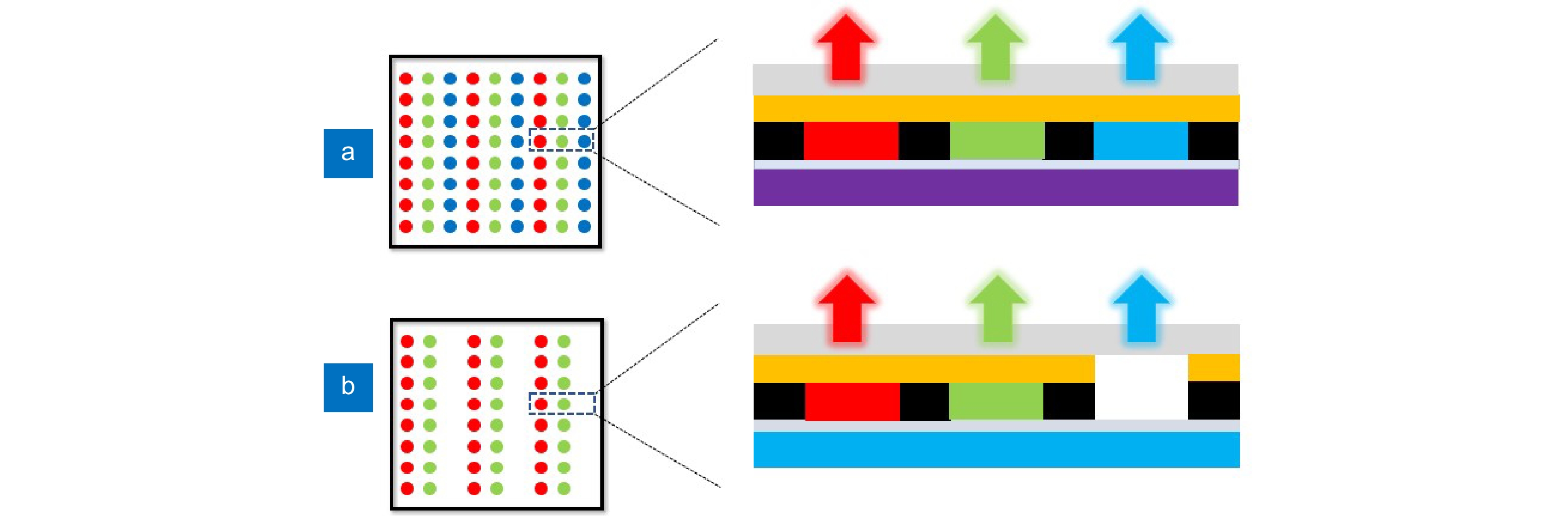
Two methods for achieving full-color by using QD CCL. (a) RBG three-color QDs excited by UV chips. (b) RG two-color QDs excited by blue chips.
-
Figure 3.
Structures of realizing the NRET from chip to QDs33. Figure reproduced with permission from John Wiley and Sons.
-
Figure 4.
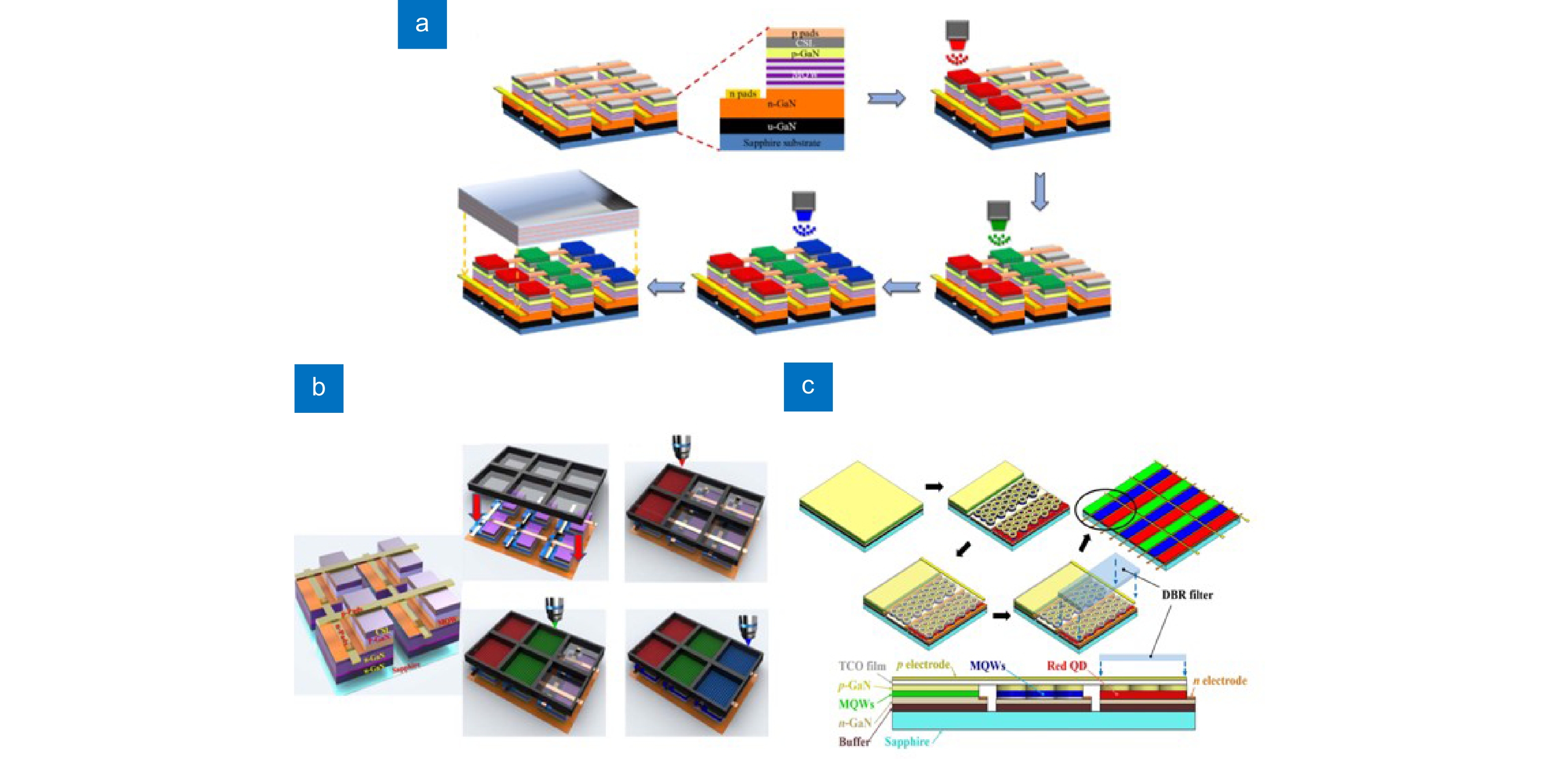
(a) Schematic diagram of AJP process. (b) Processes of fabricating the full-color micro-LED display based on lithography and AJP technique. (c) Full-color design of QD-NR-Micro-LED display. Figure reproduced with permission from: (a) ref.16, The Optical Society; (b) ref.41, (c) ref.15, Chinese Laser Press.
-
Figure 5.
(a) Sketch of the full color RGB QD-converted micro-LED array based on an UV backlight module and the device image (inset). (b) Schematic illustration of the full-color prototype . (c) Cross-section structure diagram of the prototype. Figure reproduced with permission from: (a) ref.42, American Chemical Society; (b, c) ref.45, John Wiley and Sons.
-
Figure 6.
Fluorescence images of (a) NCTU and (b) logo of XMU printed by SIJ printing. Figure reproduced with permission from: (a)15, Optica Publishing Group.
-
Figure 7.
A distribution of line widths of various inkjet printing in recent decades16–19, 42–44, 48, 50, 52–115.
-
Figure 8.
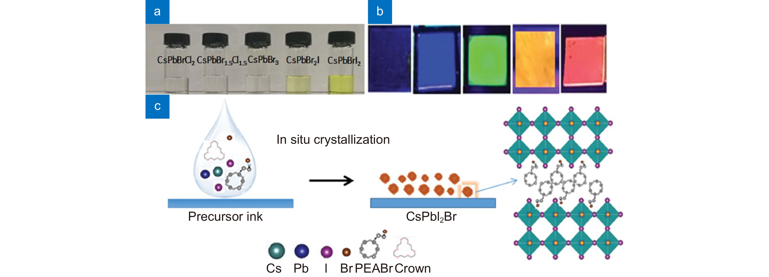
(a) Photographs of the CsPbX3 inks. (b) CsPbX3 films with different halide compositions under a 365 nm UV lamp and (c) schematic of perovskite transformation from CsPbX3 ink to CsPbX3 nanocrystal. Figure reproduced with permission from ref.19, John Wiley and Sons.
-
Figure 9.
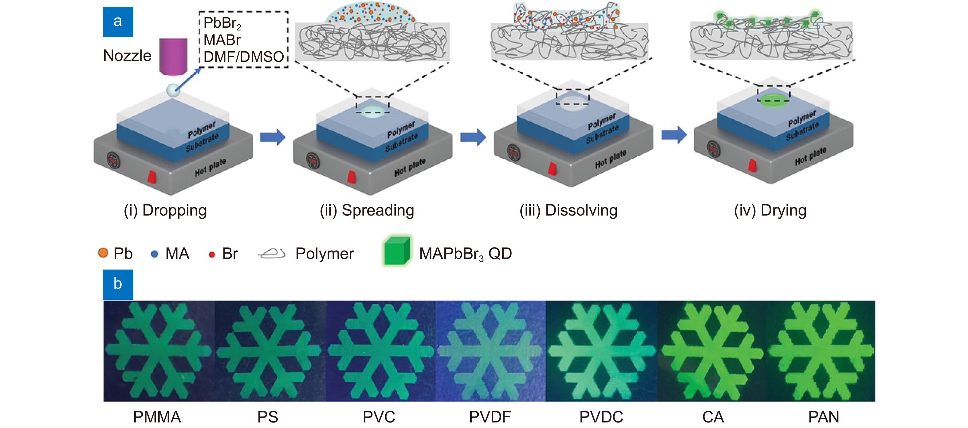
(a) Schematic diagram of the in situ inkjet printing strategy. (b) The optical images of printed PQD patterns on different polymer substrates under UV light. Figure reproduced with permission from ref.69, John Wiley and Sons.
-
Figure 10.
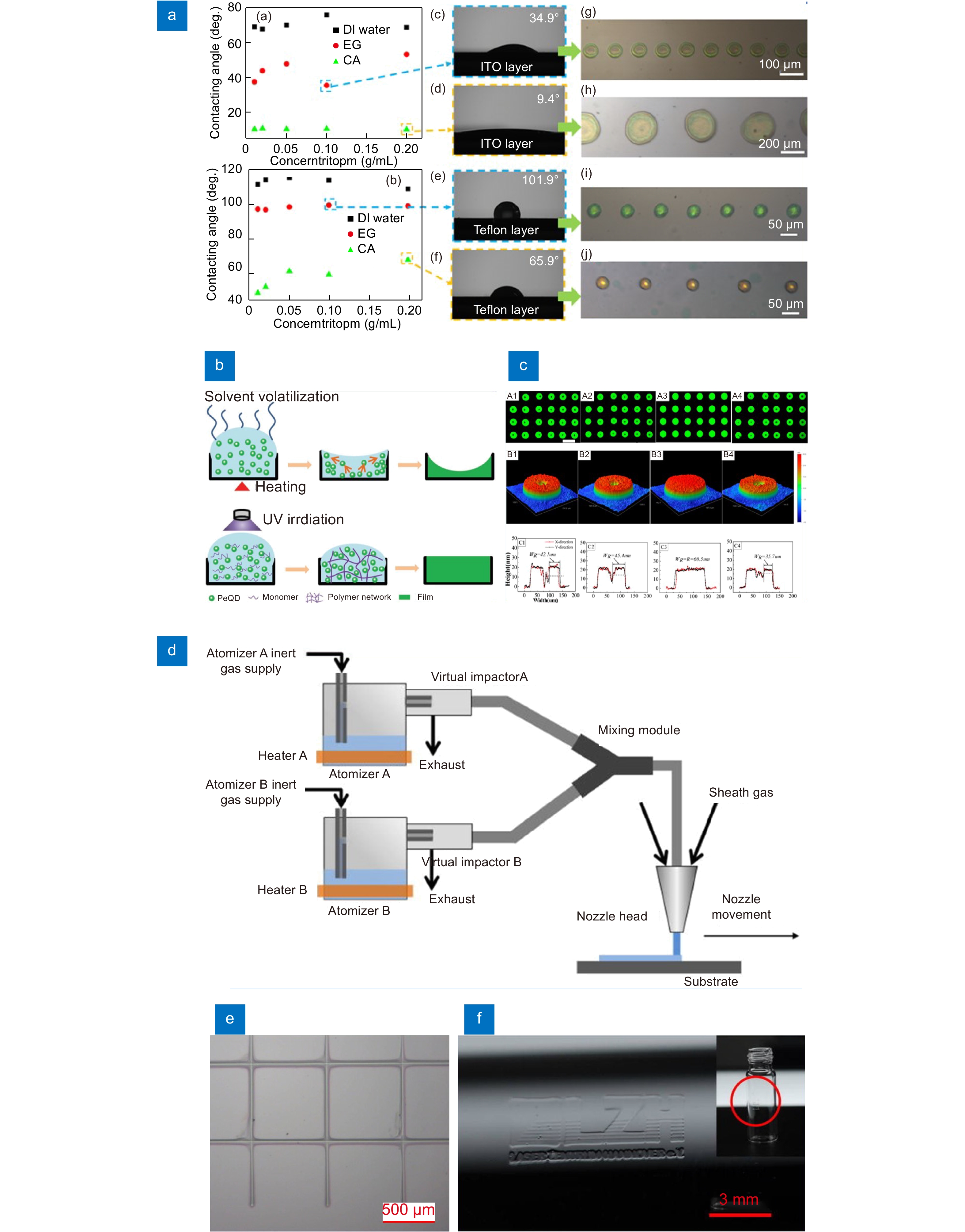
(a) Relationships between the concentrations of silica particles in colloidal inks and the contact angles of ITO glasses and silicon wafers with Teflon layers. Optical images of the latex droplets and printed photonic crystals microstructures on the ITO glasses and silicon wafers with Teflon layers. (b) Schematic illustration of the film forming process using thermal-curing and UV-curing inks, respectively. (c) PL microscopic images and 3D morphology images of dot arrays, and film thickness profile of each single dot achieved by printing quantum dots inks with volume ratios of 0, 10, 20, and 30% oDBC. (d) Fluid flow schematic of the AJP system with a dual atomizer module91. (e) Fabricated 2D patterning of a square grid on planar surfaces91. (f) LZH logo printed on a freeform cylindrical surface121. Figure reproduced with permission from: (a) ref.113, American Chemical Society; (b) ref.43, John Wiley and Sons; (c) ref.17, American Chemical Society; (d–f) ref.91, AIP Publishing.
-
Figure 11.
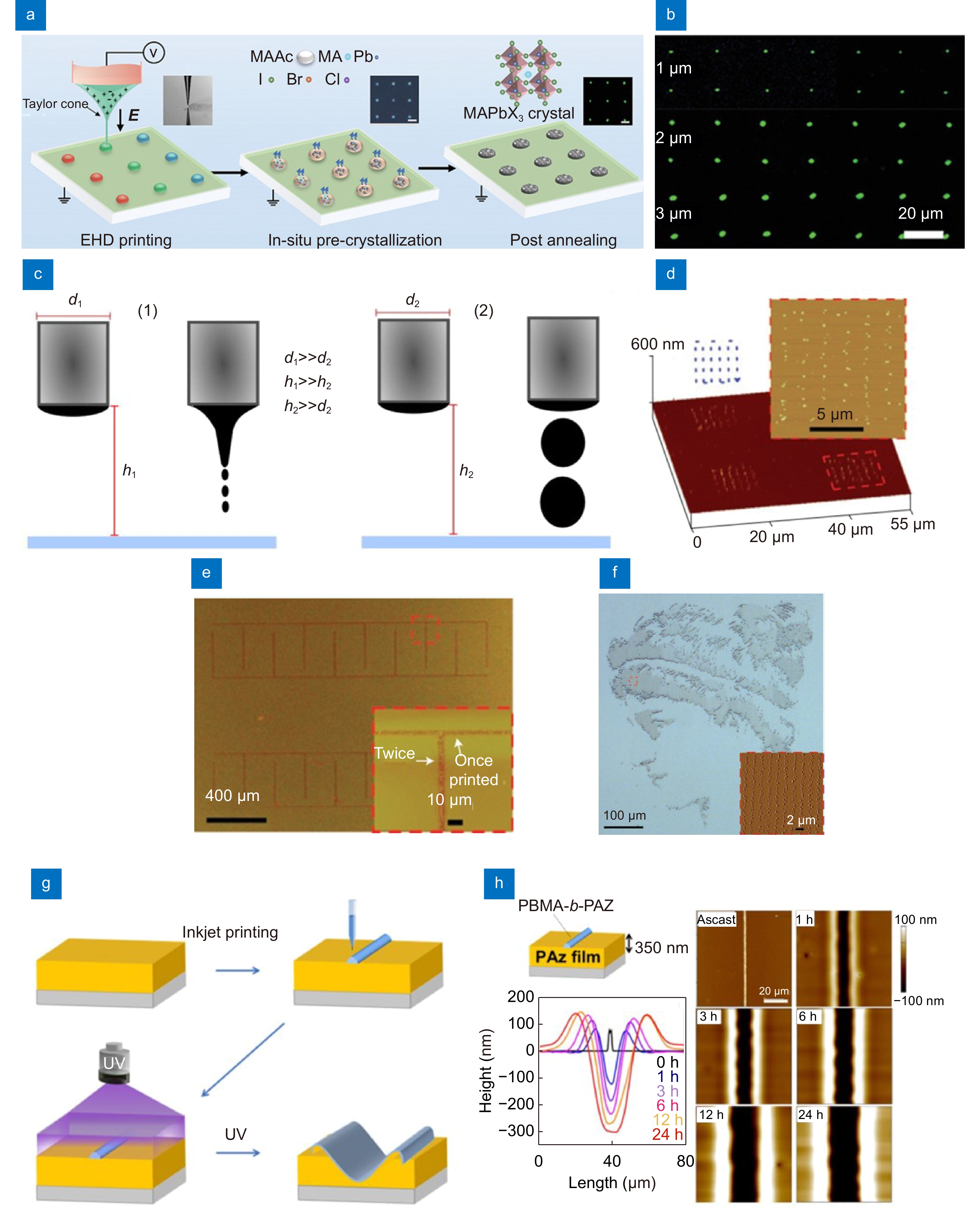
(a) Schematic illustration of the EHD inkjet printing fabrication process and perovskite transformation. (b) The EHD printed high-resolution dot array with dot diameters of 1, 2, and 3 µm respectively. (c) Printing mode of conventional EHD inkjet printing (1) vs SIJ (2) shown with and without ink charging. (d) Three-dimensional AFM image of aligned arrays of dots. (e) Continuous lines printed using the single-walled carbon nanotube ink. (f) Optical micrograph of a portrait of an ancient scholar, Hypatia, printed using a polyurethane ink. (g) Schematic of the concave (trench) formation. (h) Topographical AFM images demonstrating the mass transfer of a PAz film under UV-light irradiation and changes in the cross-sectional profile obtained from the AFM data. Figure reproduced with permission from: (a, b) ref.107, John Wiley and Sons; (c) ref.24; (d–f) 75, Springer Nature; (g, h) ref.88, under a Creative Commons Attribution 4.0 International License.
-
Figure 12.
(a) Fluorescence microphotographs and three-dimensional white light interferometer images of dot arrays printed with different PVP concentrations. (b) Fluorescence microphotographs, higher resolution fluorescence microphotographs and 3D morphology images of the white light interferometer of QD dot arrays. (c) Illustration depicting deposition mechanism and binarized experimental images of deposits of spheres, slightly stretched particles and ellipsoids. (d) SEM images of polystyrene ink drops printed in one, two, and three layers; AFM profile of deposited drops of PS 450. (e) Cross section and 3D projection from an optical profilometer of single drops at different temperatures. (f) Confocal laser scattering microscopic 3D images of dots with varying solvent compositions and corresponding two-dimensional profiles. Figure reproduced with permission from: (a) ref.112, The Royal Society of Chemistry; (b) ref.71, John Wiley and Sons; (c) ref.126, American Physical Society; (d) ref.127, John Wiley and Sons; (e) ref.128, American Chemical Society; (f) ref.129, AIP Publishing.
-
Figure 13.
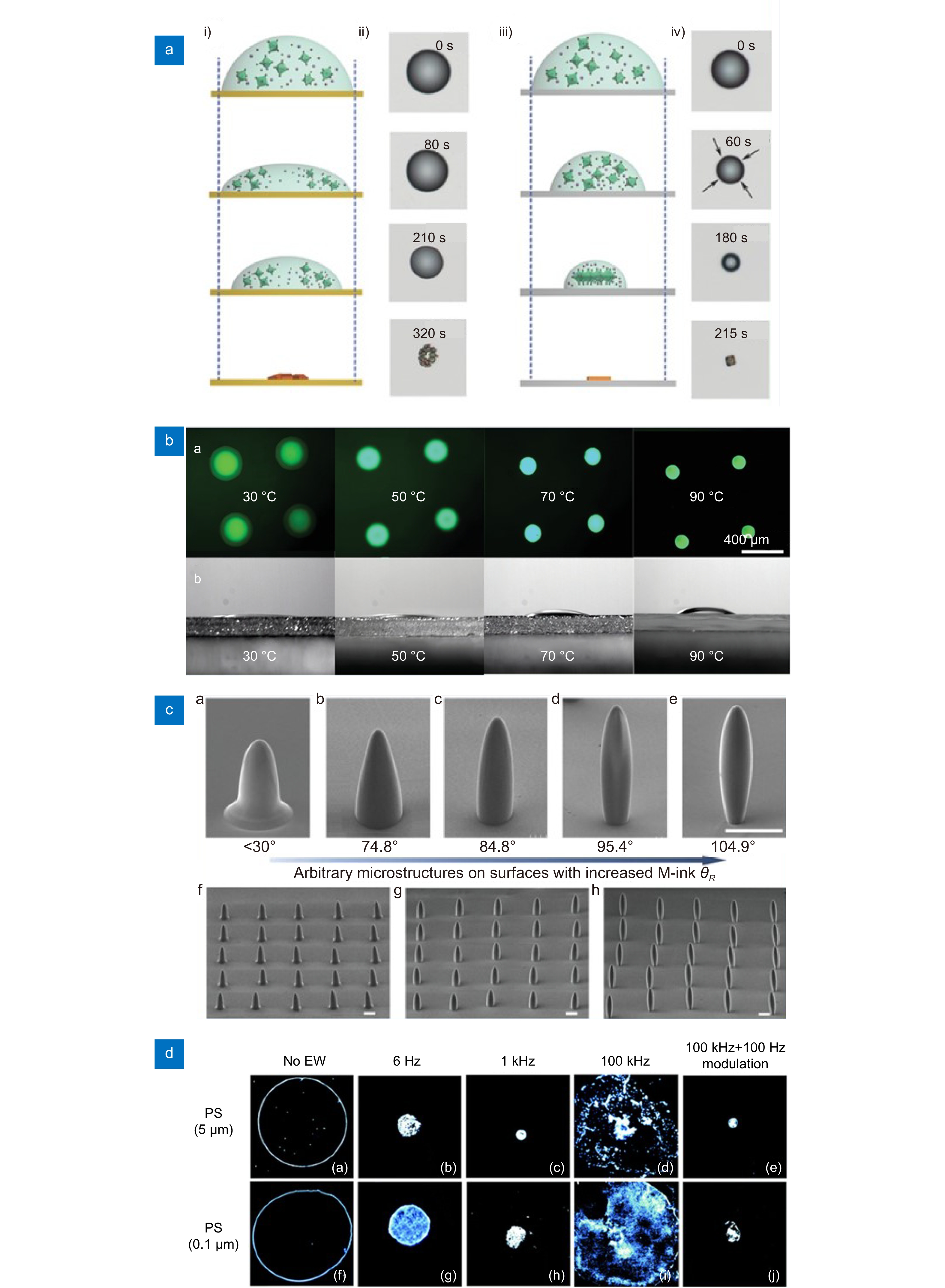
(a) Schematic illustration and optical microscopy images of the perovskite precursor droplet crystallizing on high and low adhesion substrates62. (b) The fluorescence and the contact angle images of resulting microdisks printed at different temperatures from 30 to 90 °C69. (c) Controllability of 3D microstructures by IJP on surfaces with tunable dewettability130. (d) Suppression of the coffee stain effect illustrated with different materials at three frequencies and amplitude modulation131.


