

A Fast Loss Model for Cascode GaN-FETs and Real-Time Degradation-Sensitive Control of Solid-State Transformers
 ,
,  and
and 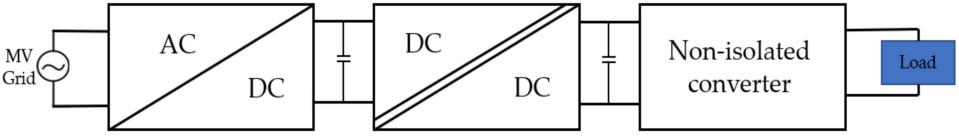
Abstract
:1. Introduction
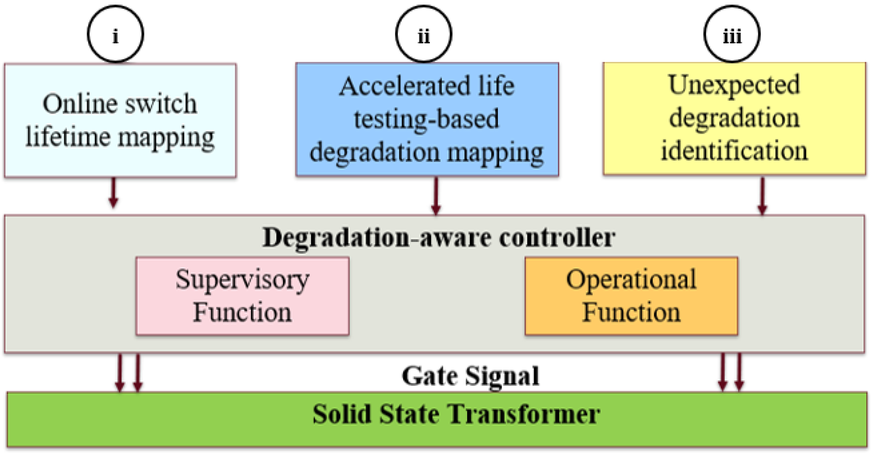
2. Principles of the Proposed Controller
- i.
- Online switch lifetime mapping;
- ii.
- Accelerated life testing (ALT)-based degradation mapping;
- iii.
- Identification of unexpected degradation.
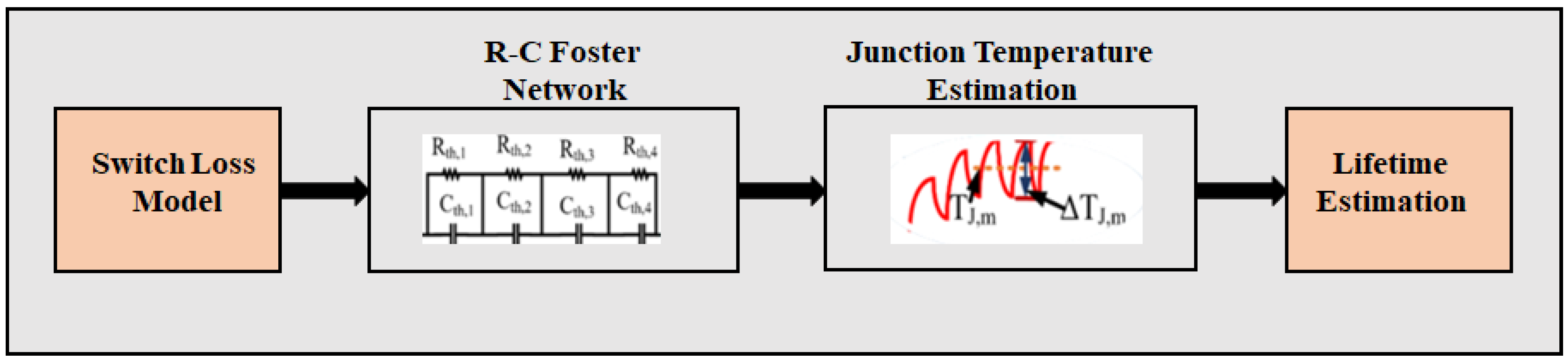
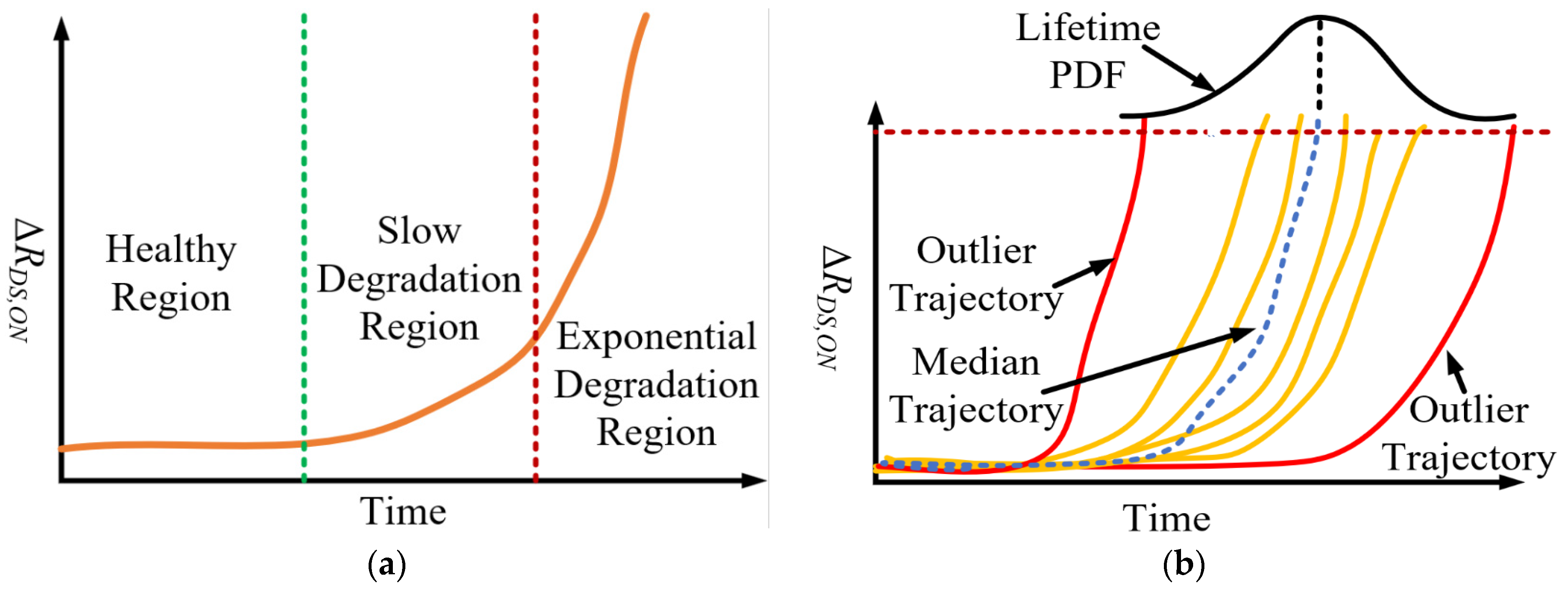
3. Online Switch Lifetime Mapping
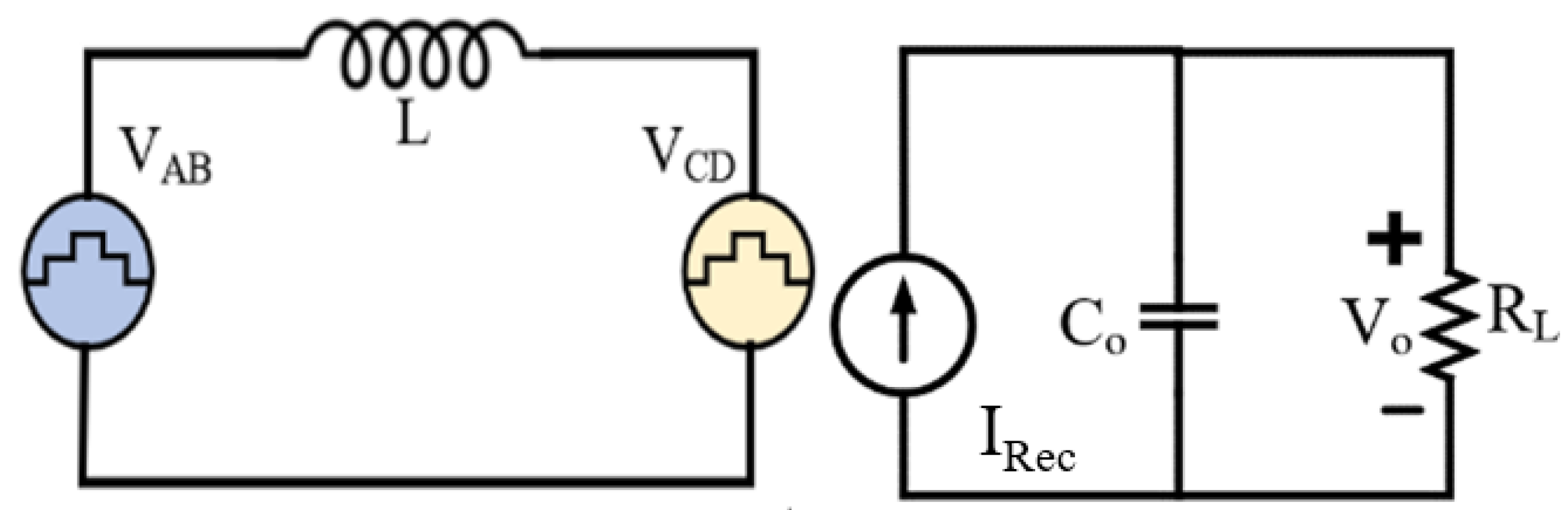
3.1. Switch Loss Model for Cascode GaN-FETs
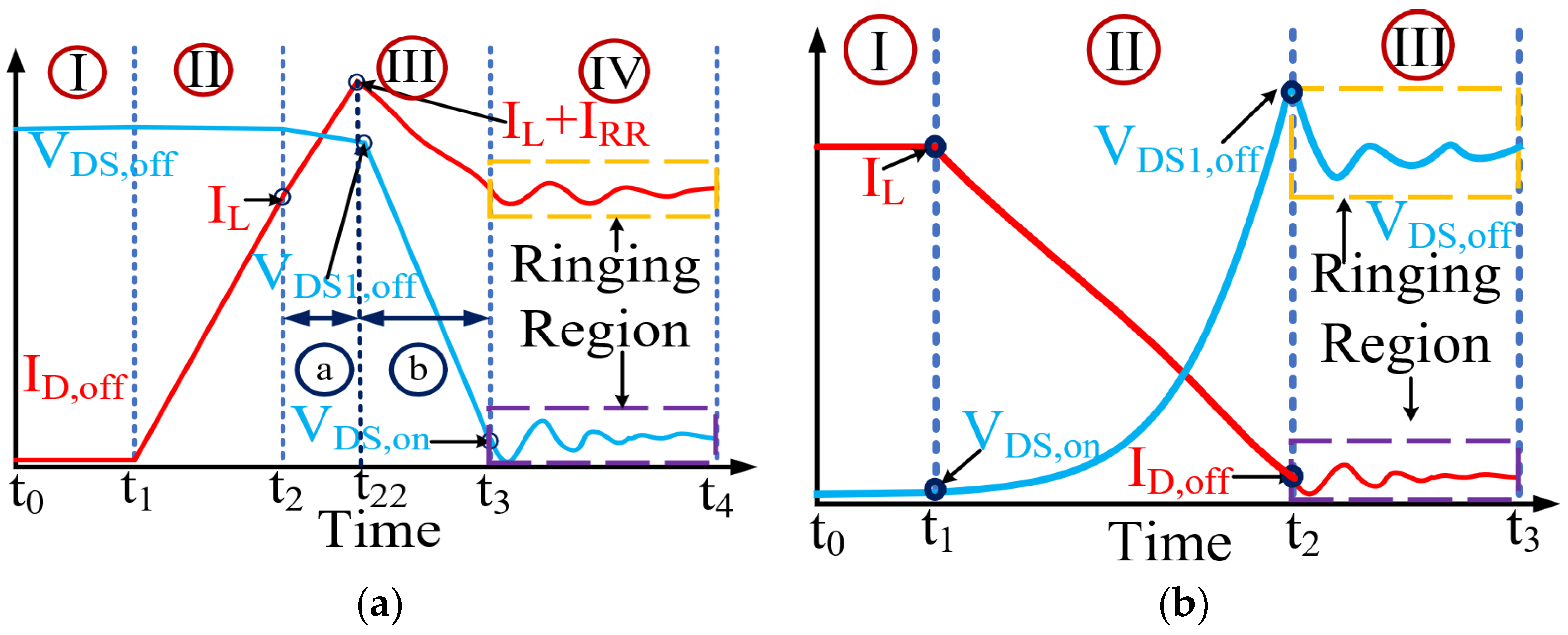
3.1.1. Turn-on Loss Calculation
- Region I: LV Si Gate Charging
- Region II: Increasing Drain Current
- Region III: Decreasing drain-source voltage
- Region IV: Ringing Region
3.1.2. Turn-off Loss Calculation
- Region-I: Gate Capacitor Discharge
- Region II: Decreasing Drain Current
- Region III: Ringing Region
3.2. R-C Foster-Model-Based Junction Temperature Estimation
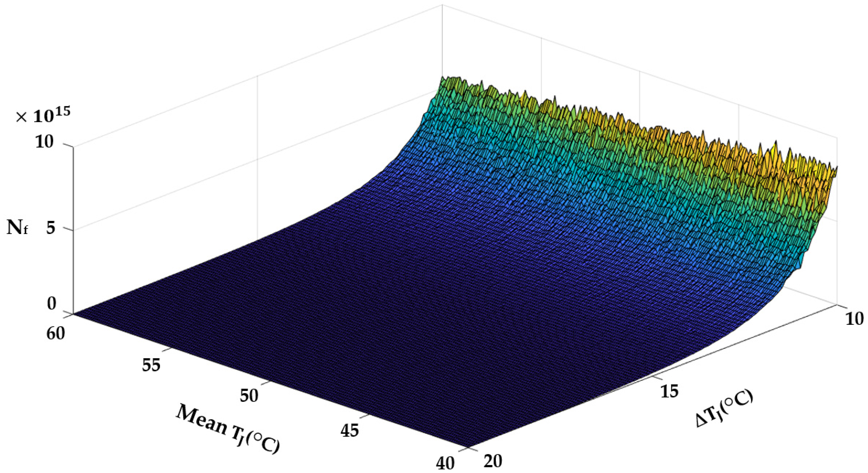
3.3. Lifetime Estimation
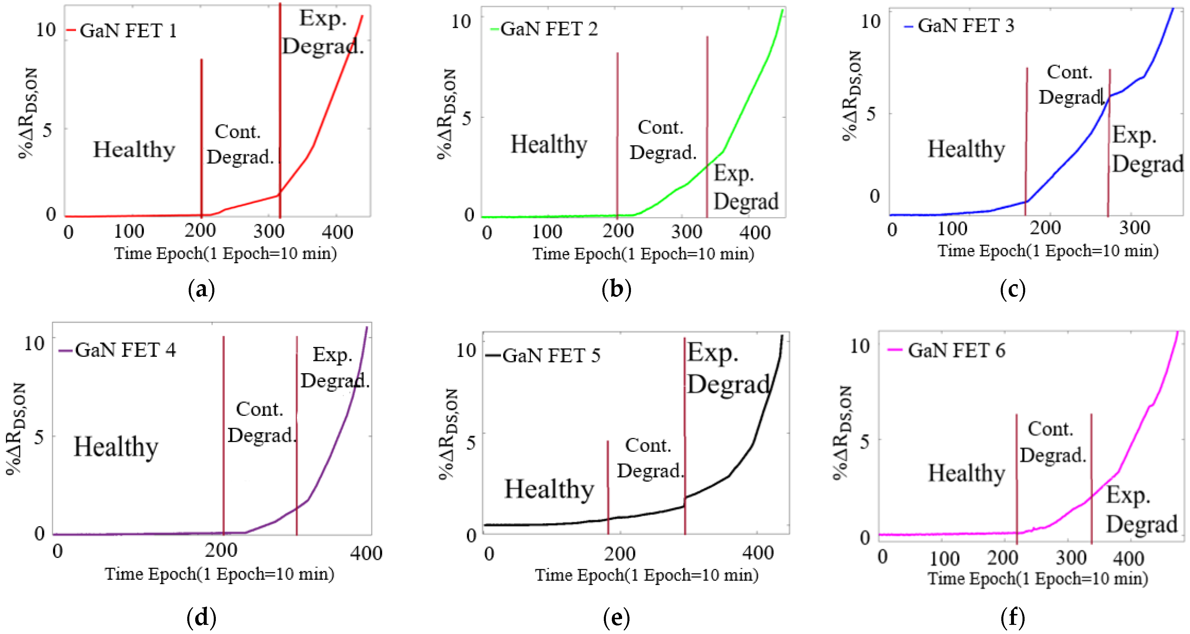
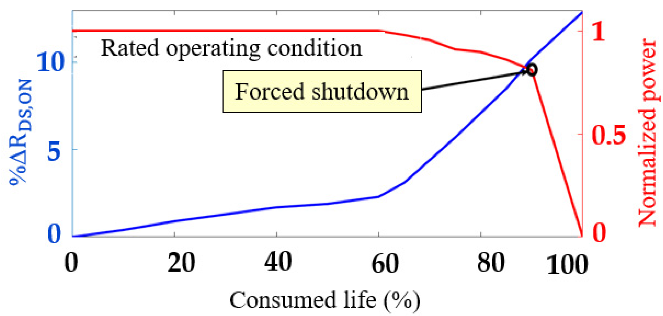
4. Degradation Mapping Based on Accelerated Life Testing
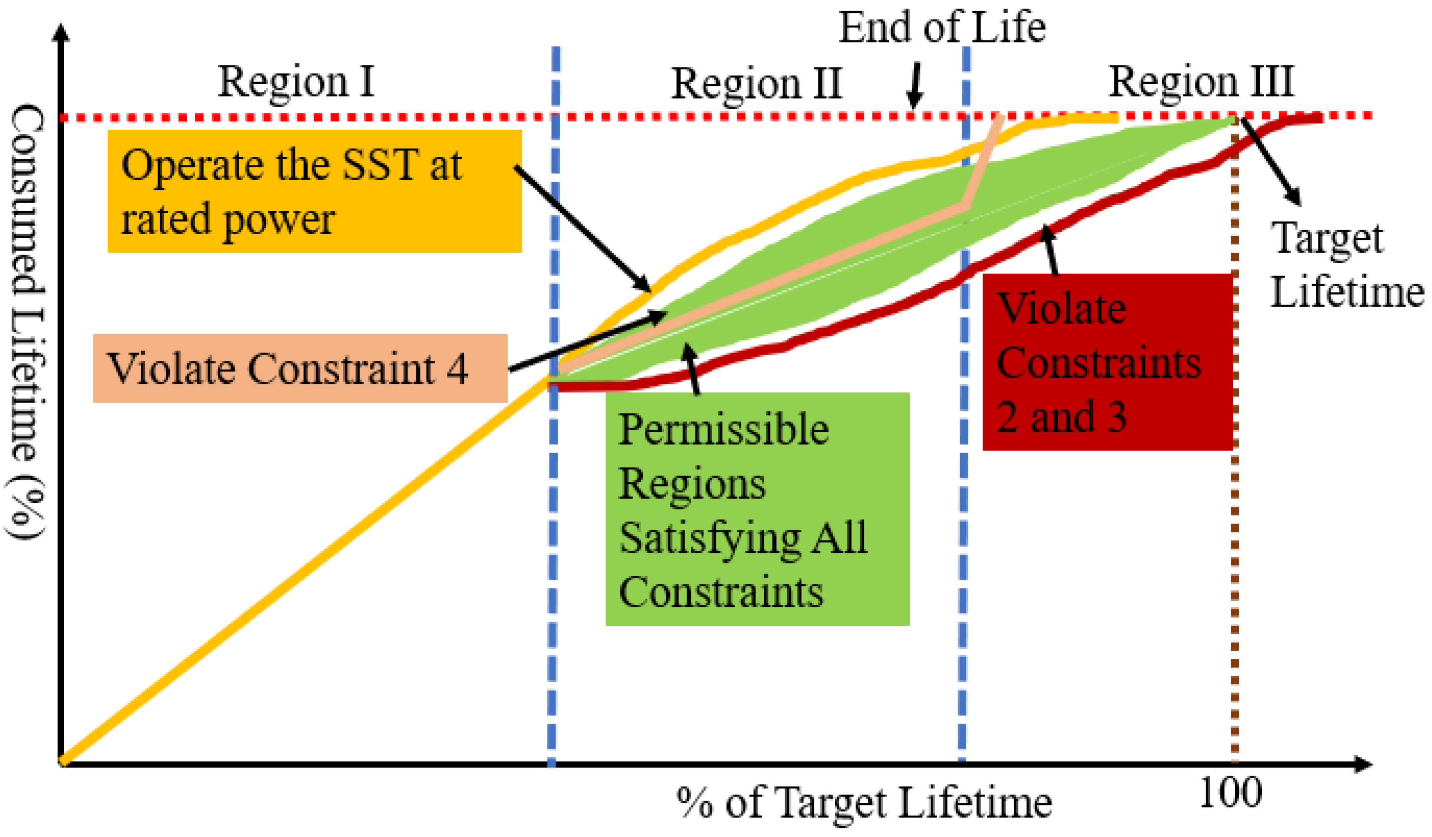
5. A Degradation-Sensitive Controller for SSTS
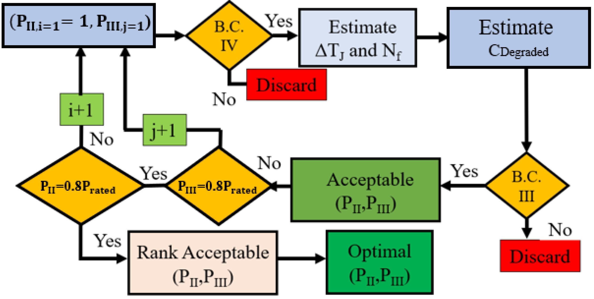
5.1. Dynamic Programmed Supervisory Function
5.2. LQR-Based Operational Function
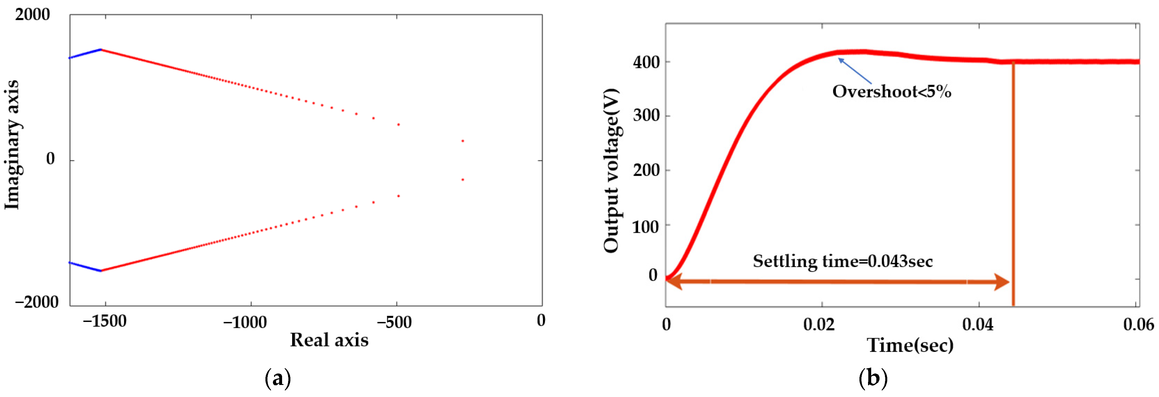
6. LQR Design and Its Performance Analysis
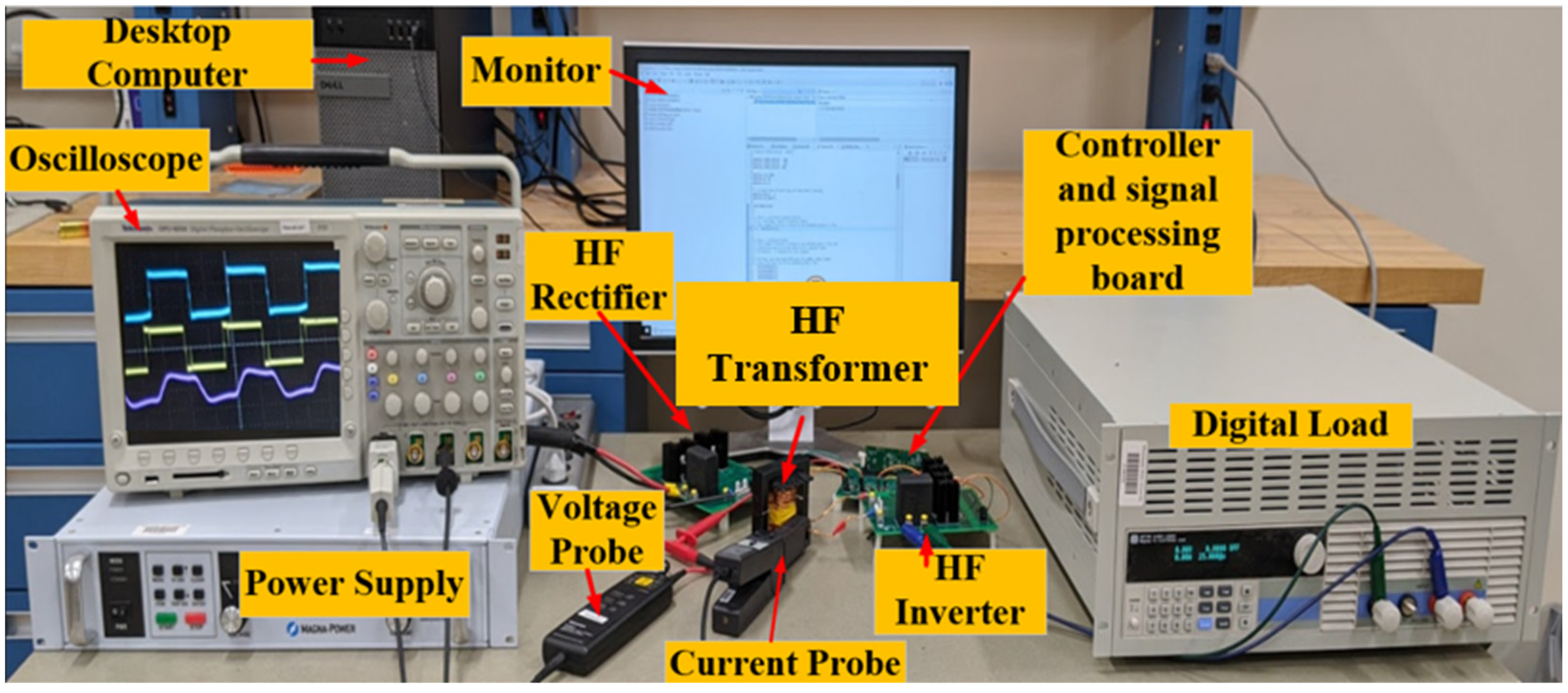
7. Experimental Testing and Validation
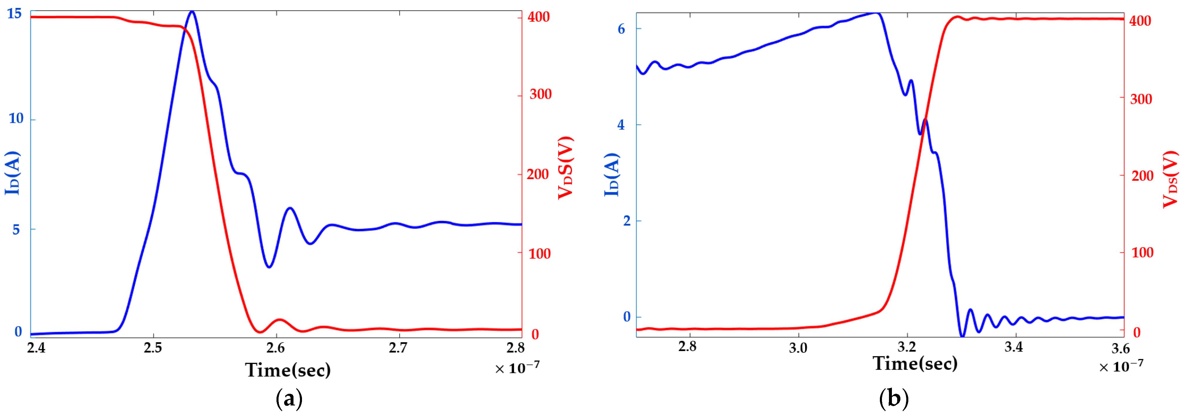
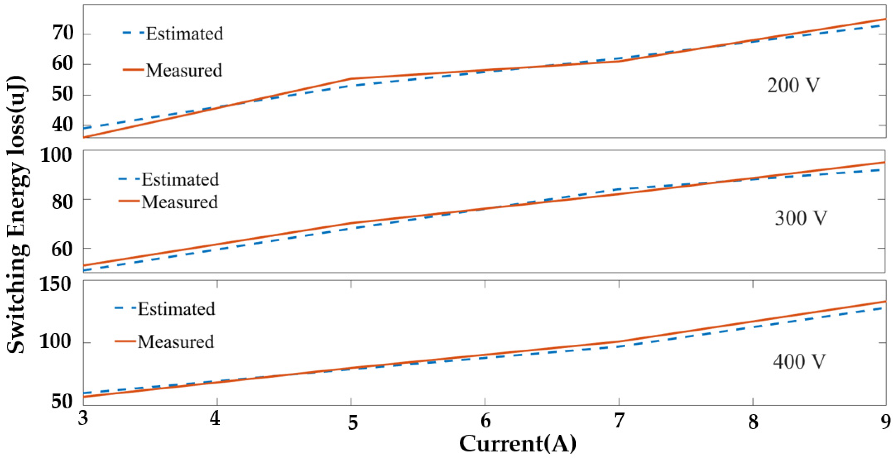
7.1. Validation of the Behavioural Switch Loss Model
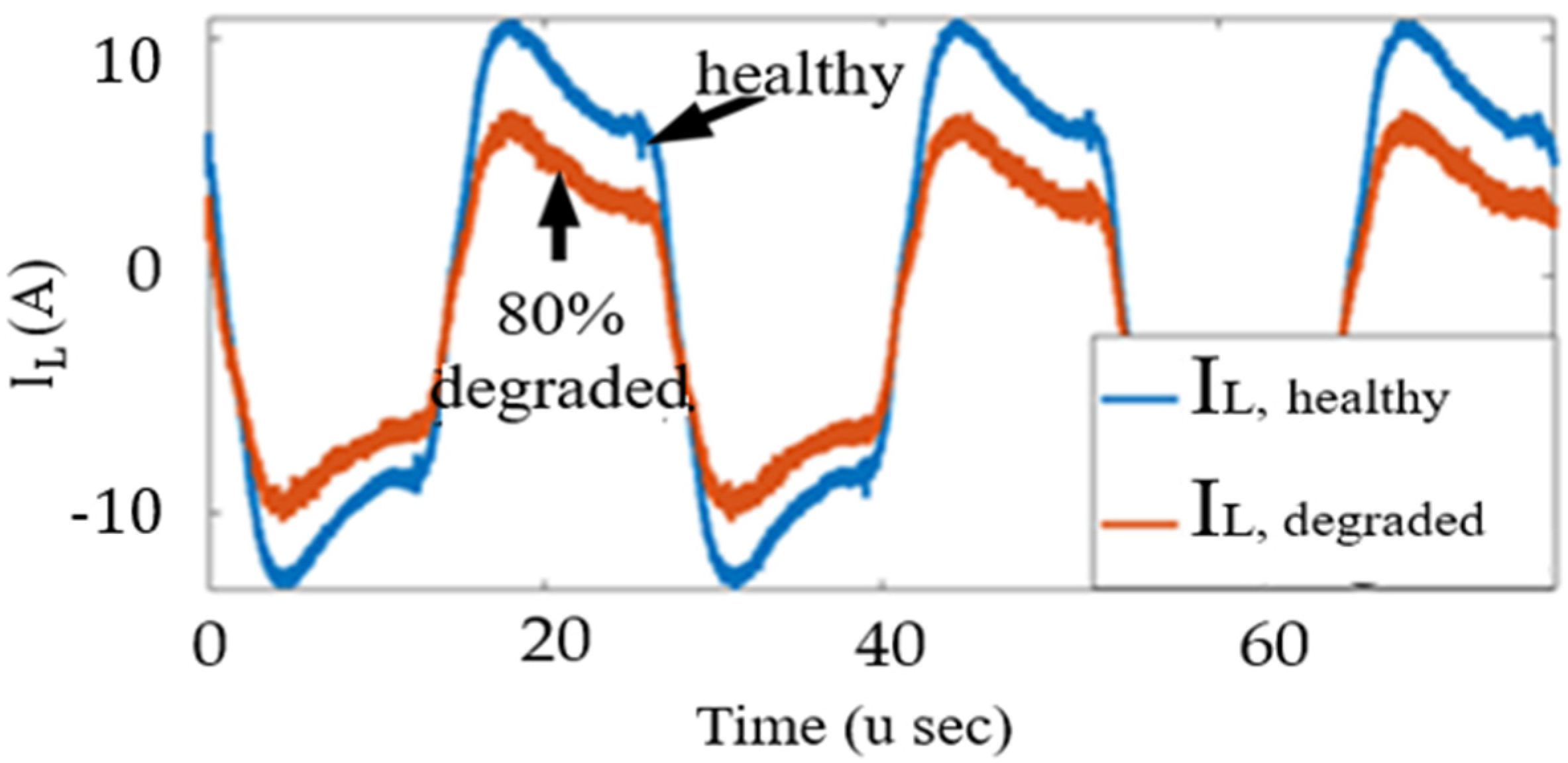
7.2. Validation of the Degradation-Sensitive Controller
8. Conclusions
Author Contributions
Funding
Institutional Review Board Statement
Informed Consent Statement
Data Availability Statement
Conflicts of Interest
References
- Shadfar, H.; Ghorbani Pashakolaei, M.; Akbari Foroud, A. Solid-state transformers: An overview of the concept, topology, and its applications in the smart grid. Int. Trans. Electr. Energy Syst. 2021, 31, 9. [Google Scholar] [CrossRef]
- Irannezhad, F.; Heydari, H. Conducting a Survey of Research on High Temperature Superconducting Transformers. IEEE Trans. Appl. Supercond. 2020, 30, 1–13. [Google Scholar] [CrossRef]
- Moradnouri, A.; Ardeshiri, A.; Vakilian, M. Survey on High-Temperature Superconducting Transformer Windings Design. J. Supercond. Nov. Magn. 2020, 33, 2581–2599. [Google Scholar] [CrossRef]
- Held, M.; Jacob, P.; Nicoletti, G.; Scacco, P.; Poech, M.-H. Fast Power Cycling Test of IGBT Modules in Traction Application. In Proceedings of the International Conference on Power Electronics and Drive Systems (PEDS), Singapore, 26–29 May 1997; pp. 1–6. [Google Scholar]
- Bayerer, R.; Herrmann, T.; Licht, T.; Lutz, J.; Feller, M. Model for Power Cycling lifetime of IGBT Modules—Various factor influencing lifetime. In Proceedings of the International Conference on Integrated Power Systems (CIPS), Virtual, 11–13 March 2008; pp. 1–6. [Google Scholar]
- Wu, F.; Feng, F.; Gooi, H.B. Cooperative Triple-Phase-Shift Control for Isolated DAB DC–DC Converter to Improve Current Characteristics. IEEE Trans. Ind. Electron. 2019, 66, 7022–7031. [Google Scholar] [CrossRef]
- Peyghami, S.; Palensky, P.; Blaabjerg, F. An Overview on the Reliability of Modern Power Electronic Based Power Systems. IEEE Open J. Power Electron. 2020, 1, 34–50. [Google Scholar] [CrossRef]
- Peyghami, S.; Wang, Z.; Blaabjerg, F. A Guideline for Reliability Prediction in Power Electronic Converters. IEEE Trans. Power Electron. 2020, 35, 10958–10968. [Google Scholar] [CrossRef]
- Wang, X.; Castellazzi, A.; Zanchetta, P. Temperature control for reduced thermal cycling of power devices. In Proceedings of the European Conference on Power Electronics and Applications (EPE), Lille, France, 2–6 September 2013; pp. 1–10. [Google Scholar]
- Lemmens, J.; Vanassche, P.; Driesen, J. Optimal Control of Traction Motor Drives Under Electrothermal Constraints. IEEE J. Emerg. Sel. Top. Power Electron. 2014, 2, 249–263. [Google Scholar] [CrossRef]
- Andresen, M.; Ma, K.; Buticchi, G.; Falck, J.; Blaabjerg, F.; Liserre, M. Junction Temperature Control for More Reliable Power Electronics. IEEE Trans. Power Electron. 2018, 33, 765–776. [Google Scholar] [CrossRef]
- Marquez, A.; Leon, J.I.; Vazquez, S.; Franquelo, L.G.; Buticchi, G.; Liserre, M. Power Device Lifetime Extension of Dc-Dc Interleaved Converters via Power Routing. In Proceedings of the IECON 2018—44th Annual Conference of the IEEE Industrial Electronics Society, Washington, DC, USA, 21–23 October 2018; pp. 5332–5337. [Google Scholar]
- Murdock, D.; Torres, J.; Connors, J.; Lorenz, R. Active thermal control of power electronic modules. IEEE Trans. Ind. Appl. 2006, 42, 552–558. [Google Scholar] [CrossRef]
- Peyghami, S.; Davari, P.; Blaabjerg, F. System-Level Reliability-Oriented Power Sharing Strategy for DC Power Systems. IEEE Trans. Ind. Appl. 2019, 55, 4865–4875. [Google Scholar] [CrossRef]
- Weckert, M.; Roth-Stielow, J. Lifetime as a control variable in power electronic systems. Emobility–Electrical Power Train, Leipzig, Germany, 8–9 November 2010; IEEE: Piscataway, NJ, USA, 2010; pp. 1–6. [Google Scholar] [CrossRef]
- Jacques, S.; Caldeira, A.; Batut, N.; Schellmanns, A.; Leroy, R.; Gonthier, L. A Coffin-Manson model to predict the TRIAC solder joints fatigue during power cycling. In Proceedings of the 2011 14th European Conference on Power Electronics and Applications, Birmingham, UK, 30 August–1 September 2011; pp. 1–8. [Google Scholar]
- Haque, M.S.; Choi, S. Support Vector Regression Assisted Auxiliary Particle Filter based Remaining Useful Life Estimation of GaN FET. In Proceedings of the IECON 2018—44th Annual Conference of the IEEE Industrial Electronics Society, Washington, DC, USA, 21–23 October 2018; pp. 1525–1530. [Google Scholar]
- Xu, C.; Ugur, E.; Yang, F.; Pu, S.; Akin, B. Investigation of Performance Degradation in Enhancement-Mode GaN HEMTs under Accelerated Aging. In Proceedings of the 2018 IEEE 6th Workshop on Wide Bandgap Power Devices and Applications (WiPDA), Atlanta, GA, USA, 31 October–2 November 2018; pp. 98–102. [Google Scholar]
- Haque, M.S.; Choi, S. Sparse Kernel Ridge Regression Assisted Particle Filter Based Remaining Useful Life Estimation of Cascode GaN FET. IEEE Trans. Ind. Electron. 2020, 68, 7516–7525. [Google Scholar] [CrossRef]
- Gareau, J.; Hou, R.; Emadi, A. Review of Loss Distribution, Analysis, and Measurement Techniques for GaN HEMTs. IEEE Trans. Power Electron. 2020, 35, 7405–7418. [Google Scholar] [CrossRef]
- Christen, D.; Biela, J. Analytical Switching Loss Modeling Based on Datasheet Parameters for mosfets in a Half-Bridge. IEEE Trans. Power Electron. 2019, 34, 3700–3710. [Google Scholar] [CrossRef]
- Huang, X.; Li, Q.; Liu, Z.; Lee, F.C. Analytical Loss Model of High Voltage GaN HEMT in Cascode Configuration. IEEE Trans. Power Electron. 2014, 29, 2208–2219. [Google Scholar] [CrossRef]
- Li, Q.; Liu, B.; Duan, S.; Wang, L.; Xu, B.; Luo, C. Analytical Switching Loss Model of Cascode GaN HEMTs Based Totem-Pole PFC Converters Considering Stray Inductances. In Proceedings of the 2018 1st Workshop on Wide Bandgap Power Devices and Applications in Asia, Xi’an, China, 16–18 May 2018; pp. 118–124. [Google Scholar]
- Xin, Y.; Chen, W.; Sun, R.; Shi, Y.; Liu, C.; Xia, Y.; Wang, F.; Maolin, L.; Li, J.; Zhou, Q.; et al. Analytical Switching Loss Model for GaN-Based Control Switch and Synchronous Rectifier in Low-Voltage Buck Converters. IEEE J. Emerg. Sel. Top. Power Electron. 2019, 7, 1485–1495. [Google Scholar] [CrossRef]
- Murillo Carrasco, L.C.; Forsyth, A.J. Energy Analysis and Performance Evaluation of GaN Cascode Switches in An Inverter Leg Configuration. In Proceedings of the 2015 IEEE Applied Power Electronics Conference and Exposition (APEC), Charlotte, NC, USA, 15–19 March 2015; pp. 2424–2431. [Google Scholar]
- Huang, X.; Liu, Z.; Lee, F.C.; Li, Q. Characterization and Enhancement of High-Voltage Cascode GaN Devices. IEEE Trans. Electron. Devices 2014, 62, 270–277. [Google Scholar] [CrossRef]


Disclaimer/Publisher’s Note: The statements, opinions and data contained in all publications are solely those of the individual author(s) and contributor(s) and not of MDPI and/or the editor(s). MDPI and/or the editor(s) disclaim responsibility for any injury to people or property resulting from any ideas, methods, instructions or products referred to in the content. |
© 2023 by the authors. Licensee MDPI, Basel, Switzerland. This article is an open access article distributed under the terms and conditions of the Creative Commons Attribution (CC BY) license (https://creativecommons.org/licenses/by/4.0/).
Share and Cite
Haque, M.S.; Moniruzzaman, M.; Choi, S.; Kwak, S.; Okilly, A.H.; Baek, J. A Fast Loss Model for Cascode GaN-FETs and Real-Time Degradation-Sensitive Control of Solid-State Transformers. Sensors 2023, 23, 4395. https://doi.org/10.3390/s23094395
Haque MS, Moniruzzaman M, Choi S, Kwak S, Okilly AH, Baek J. A Fast Loss Model for Cascode GaN-FETs and Real-Time Degradation-Sensitive Control of Solid-State Transformers. Sensors. 2023; 23(9):4395. https://doi.org/10.3390/s23094395
Chicago/Turabian StyleHaque, Moinul Shahidul, Md Moniruzzaman, Seungdeog Choi, Sangshin Kwak, Ahmed H. Okilly, and Jeihoon Baek. 2023. "A Fast Loss Model for Cascode GaN-FETs and Real-Time Degradation-Sensitive Control of Solid-State Transformers" Sensors 23, no. 9: 4395. https://doi.org/10.3390/s23094395