F-Shaped Tunnel Field-Effect Transistor (TFET) for the Low-Power Application
by
 ,
,
Seunghyun Yun
1, 
Jeongmin Oh
1,
Seokjung Kang
1,
Yoon Kim
2,
Jang Hyun Kim
3,
Garam Kim
4 and
Sangwan Kim
1,* 1
Department of Electrical and Computer Engineering, Ajou University, Suwon 16499, Korea
2
School of Electrical and Computer Engineering, University of Seoul, Seoul 02504, Korea
3
Inter-university Semiconductor Research Center, Department of Electrical and with the Department of Computer Engineering, Seoul National University, Seoul 08826, Korea
4
Department of Electronic Engineering, Myongji University, Yongin 17058, Korea
*
Author to whom correspondence should be addressed.
Micromachines 2019, 10(11), 760; https://doi.org/10.3390/mi10110760
Submission received: 12 October 2019
/
Revised: 31 October 2019
/
Accepted: 7 November 2019
/
Published: 9 November 2019
(This article belongs to the Special Issue Extremely-Low-Power Devices and Their Applications)
Abstract
:In this report, a novel tunnel field-effect transistor (TFET) named ‘F-shaped TFET’ has been proposed and its electrical characteristics are analyzed and optimized by using a computer-aided design simulation. It features ultra-thin and a highly doped source surrounded by lightly doped regions. As a result, it is compared to an L-shaped TFET, which is a motivation of this work, the F-shaped TFET can lower turn-on voltage (VON) maintaining high on-state current (ION) and low subthreshold swing (SS) with the help of electric field crowding effects. The optimized F-shaped TFET shows 0.4 V lower VON than the L-shaped TFET with the same design parameter. In addition, it shows 4.8 times higher ION and 7 mV/dec smaller average SS with the same VON as that for L-shaped TFET.
1. Introduction
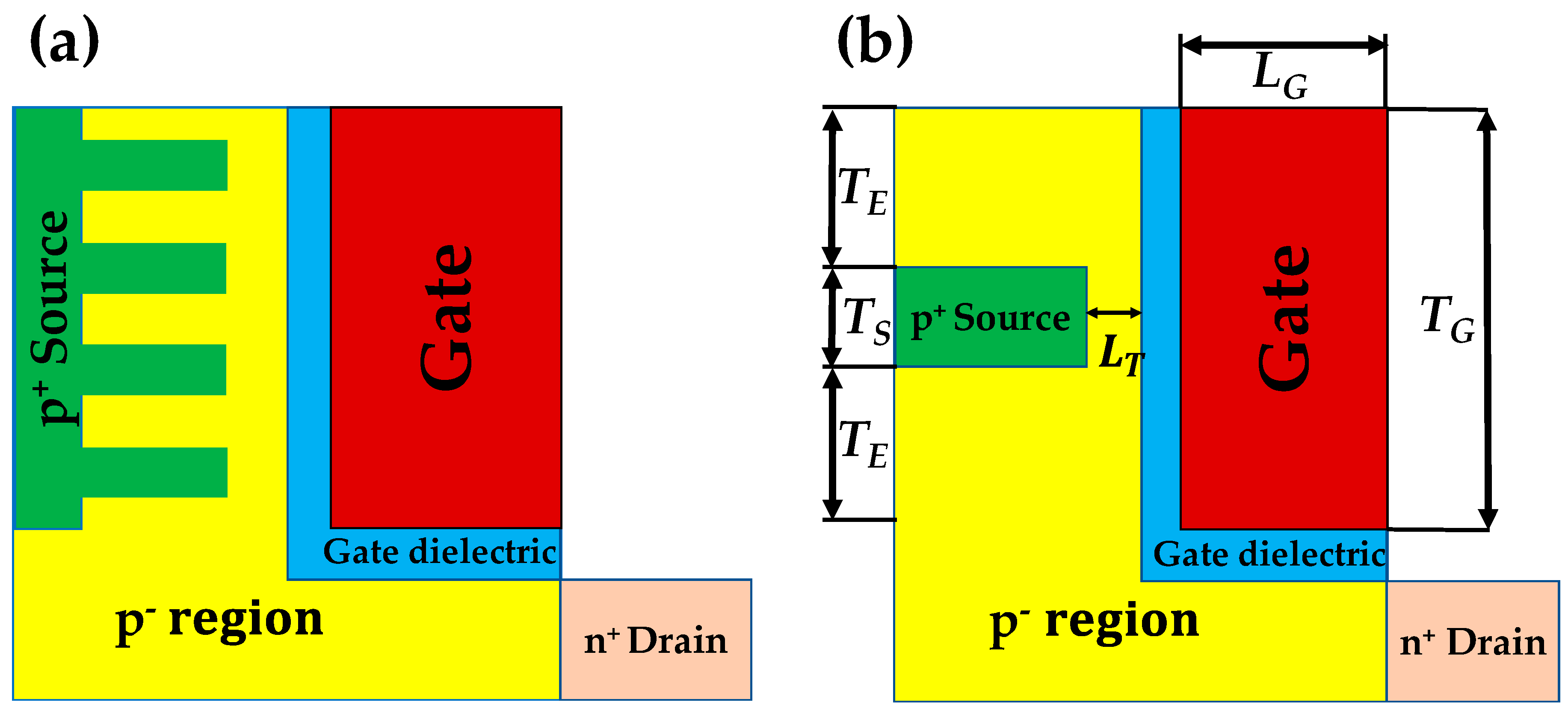
Tunnel field-effect transistor (TFET) has been regarded as a promising candidate to replace the metal-oxide-semiconductor FET (MOSFET) for a low power device because its subthreshold swing (SS) can be scaled less than 60 mV/dec [1,2,3,4,5,6,7,8]. However, Si-based TFET suffers from low-level on-state current (ION) due to its limited band-to-band tunneling (BTBT) rate. Furthermore, there are just a few reports which have demonstrated sub-60 mV/dec SS with the experimental devices. Several strategies have been proposed to address these issues [9,10,11,12,13,14,15,16,17,18,19]. Among them, L-shaped TFET has efficiently improved ION and SS by increasing BTBT junction area and by decreasing BTBT barrier width (WTUN) with the help of a novel structure [20]. In spite of these advantages, there is a drawback that turn-on voltage (VON), which is defined as gate voltage (VGS) when BTBT starts to occur, becomes much higher than conventional TFET. It is contradictory to apply the low-power logic elements [21,22]. Therefore, in this manuscript, a new-structure TFET is proposed to address the technical issue of L-shaped TFET maintaining its advantages. Figure 1a shows a schematic structure of proposed device named ‘F-shaped TFET’ because the shape of source is similar to the fingers. It resembles an L-shaped TFET except the ultra-thin sources which are surrounded by intrinsic (or lightly doped) Si regions [20]. It is expected that the F-shaped TFET can reduce VON with the help of electric field crowding effect as the thickness of source (TS) gets thinner. In order to examine the electrical characteristics of F-shaped TFET, technology computer-aided design (TCAD) simulation is performed [23]. Nonlocal BTBT, Shockley–Read–Hall recombination, bandgap narrowing, and concentration-dependent mobility models are considered for an accurate examination. Table 1 shows the parameters used for the simulation. Gate length (LG) is set by 20 nm and drain regions are lightly doped to suppress ambipolar behavior.
This manuscript is composed as follows. First, the electrical performance of the F-shaped TFET with a single-source region (i.e., one finger) is examined (Figure 1b). Many parameters such as TS, lateral length of tunnel region (LT), and space above and below source (TE) have been set as variables. In Section 2, the influences of TS, LT, and TE have been discussed. In Section 3, feasibility for the better performance with F-shaped TFET is examined by adding one more source region (i.e., two fingers) and its design is optimized by adjusting the distance between two source regions (TI). In Section 4, the optimized design is compared with the conventional L-shaped TFET. In Section 5, an exemplary process flow for the fabrication of F-shaped TFET is proposed.
2. Influences of Design Parameters
2.1. Length of Tunnel Region (LT)
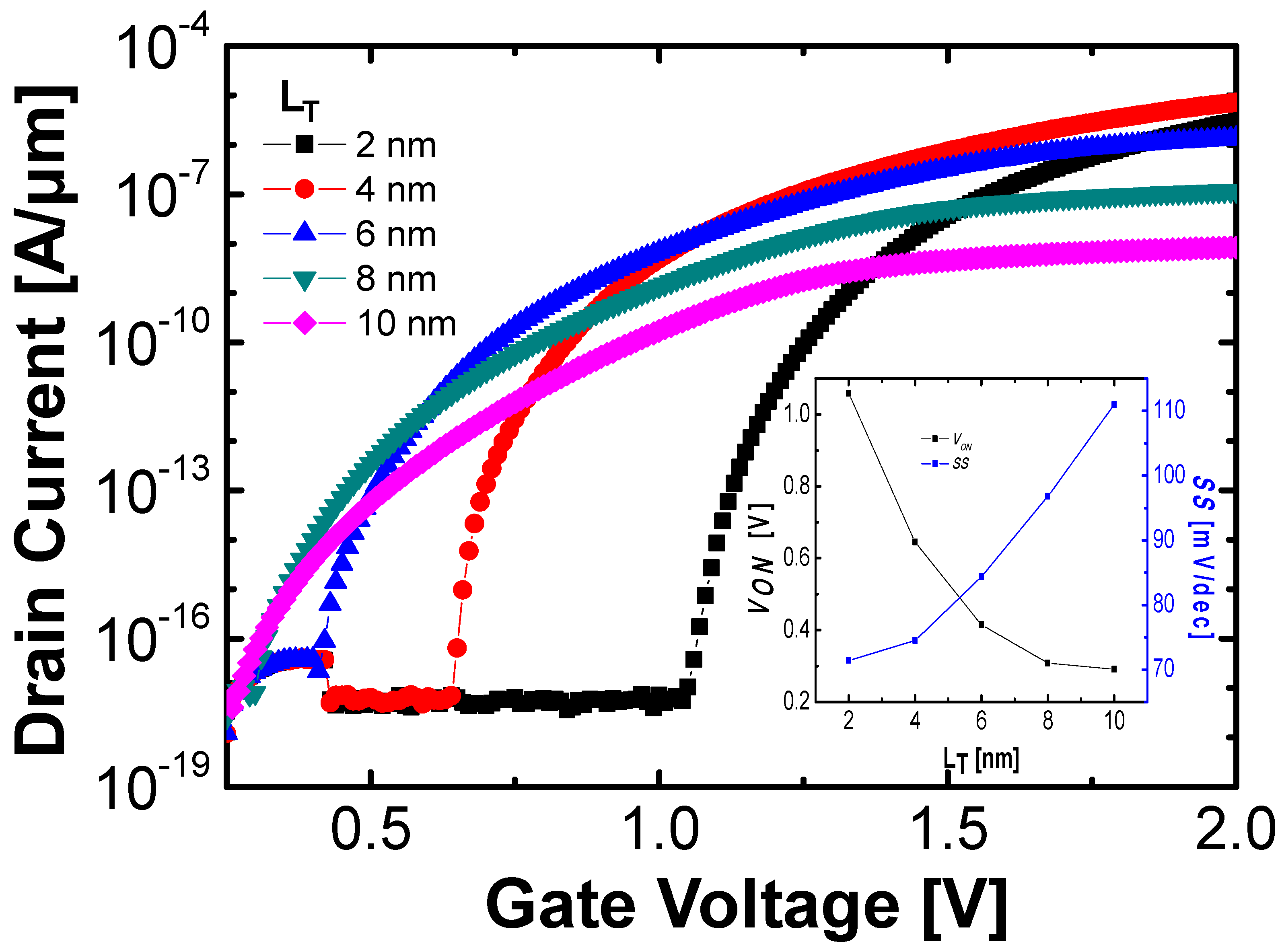
Figure 2 shows transfer characteristics as LT changes from 10 to 2 nm. It shows that VON increases as LT decreases. This is explained by the surface potential depending on LT with the help of the voltage division model in series-connected capacitors [24]. In detail, if LT decreases, the surface potential at the fixed VGS is reduced because the capacitance of the fully depleted Si tunnel region increases; results in a high VON. On the other hand, the average SS (SSAVG) decreases if LT decreases (Figure 2 and its inset). It is attributed to the smaller WTUN (at VGS = VON) with the smaller LT [24]. Similarly, Ion increases as LT decreases, because the WTUN at on-state decreases. The optimum LT is determined as 4 nm, since the increase of VON is significant while the reduction of SSAVG is negligible as LT becomes less than 4 nm (inset of Figure 2).
2.2. Source Thickness (TS)
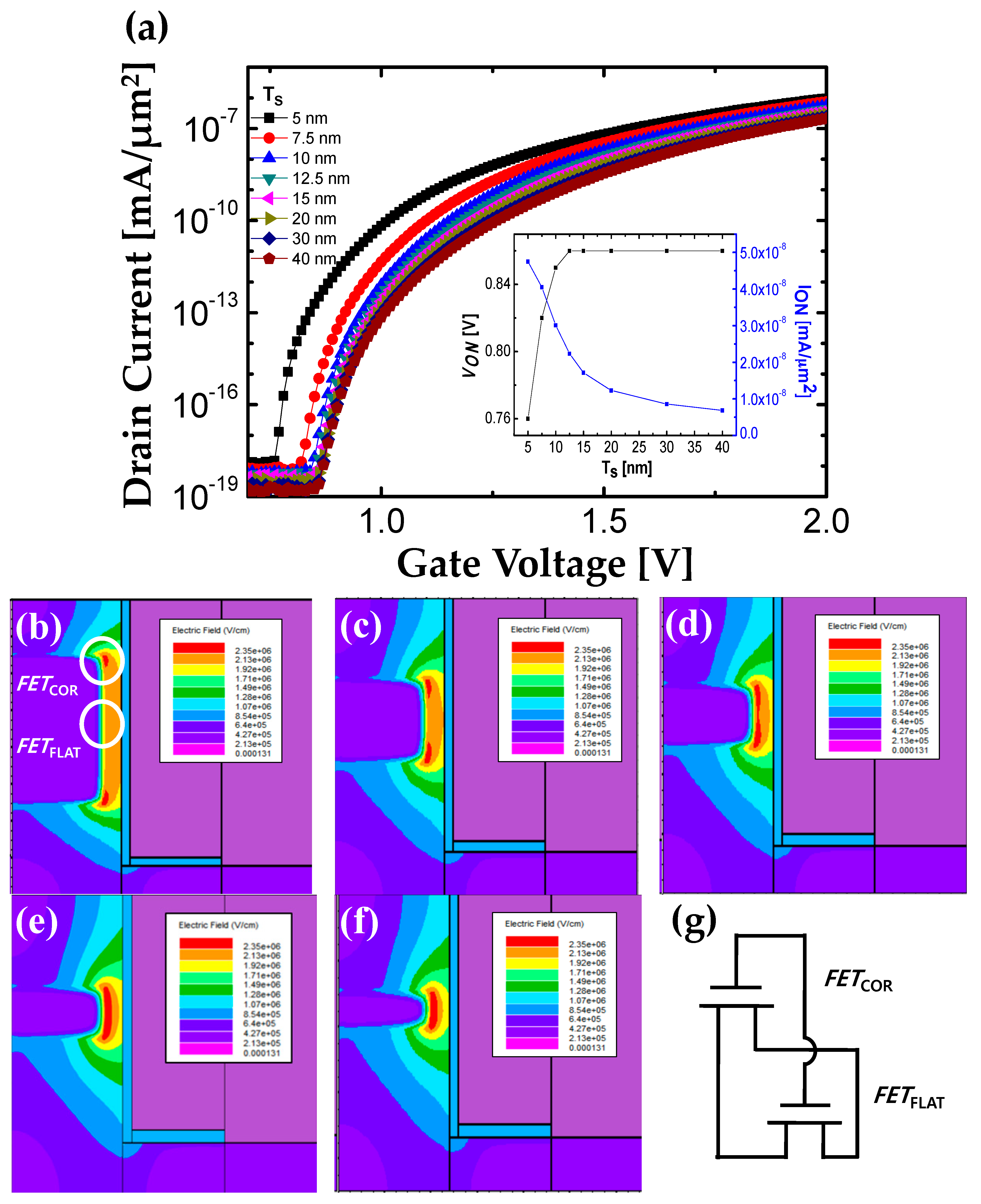
Figure 3a shows transfer characteristics depending on TS. The drain current (ID) is normalized by TS to exclude the influence of TS on the BTBT junction area and on the magnitude of ID. There are two noteworthy points in terms of ION and VON as shown in the inset of Figure 3a. Both results can be analyzed by electric field contour plots shown in Figure 3b–f. As shown in Figure 3b, electric field at sharp source corner (ECOR) is much larger than that for flat source region (EFLAT) due to field crowding effect [25]. Because VON and ION of TFETs sensitively depend on electric field at source-to-channel junction, the source corner and the flat source regions can be regarded as different TFETs; FETCOR and FETFLAT. In other words, F-shaped TFET can be regarded as FETCOR and FETFLAT connected in parallel as shown in Figure 3g. If TS decreases, the FETCOR contributes more to ID than FETFLAT. As a result, the normalized ID by TS is increased because FETCOR has higher current than FETFLAT.
Unlike to ION, VON is solely determined by FETCOR which is turned on first. Although TS decreases (i.e., the portion of FETCOR increases), the ECOR is unchanged. Therefore, VON is not affected by TS from 40 to 10 nm (Figure 3b–d). On the other hand, if TS becomes less than 10 nm, FETFLAT is completely disappeared and FETCOR at two corners starts to be merged (Figure 3e,f). As a result, the magnitude of electric field is increased further and VON starts to be decreased. Considering process capability, TS is optimized as 5 nm.
2.3. Space Above and Below Source (TE)
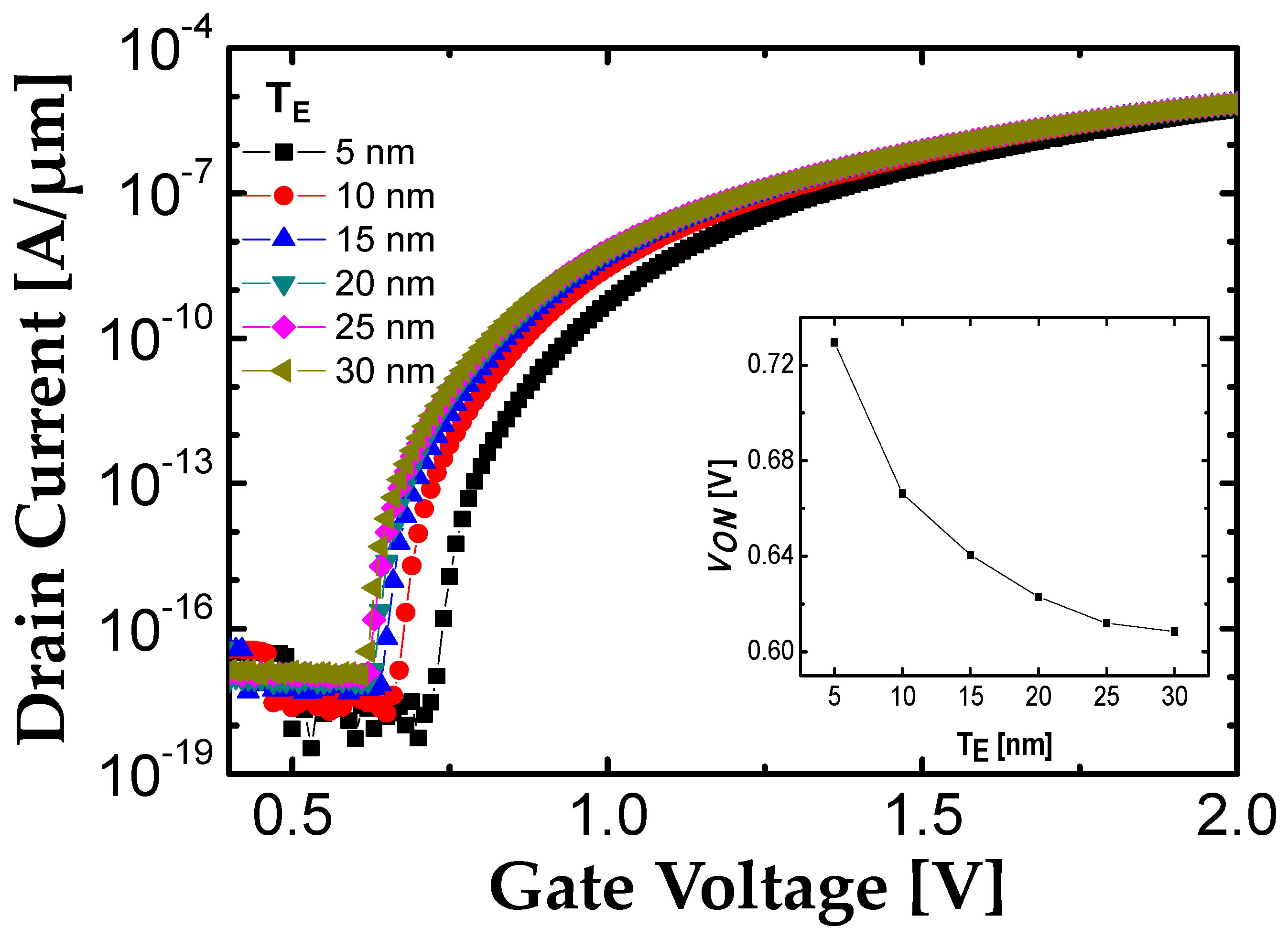
As discussed in Figure 1, unlike the L-shaped TFET, the source of the F-shaped TFET is surrounded by lightly doped Si regions. Therefore, it is worthwhile to study about the influence of TE on electrical characteristics of F-shaped TFET because it can influence on electric field crowding. As shown in Figure 4, the VON slightly decreases as the TE increases due to the increase of electric field crowding effect. In other word, the number of electric field flux is increased since the tunnel junction is affected by the larger gate area. Consequently, band bending at tunnel junction becomes abrupt, and hence decreases VON. However, large TE is contradictory to the process capability (i.e., abrupt etching profile). In addition, if TE increases more than 15 nm, the decrease of VON is negligible as shown in the inset of Figure 4. Based on the above results, TE is optimized as 15 nm.
3. Optimized F-Shaped TFET
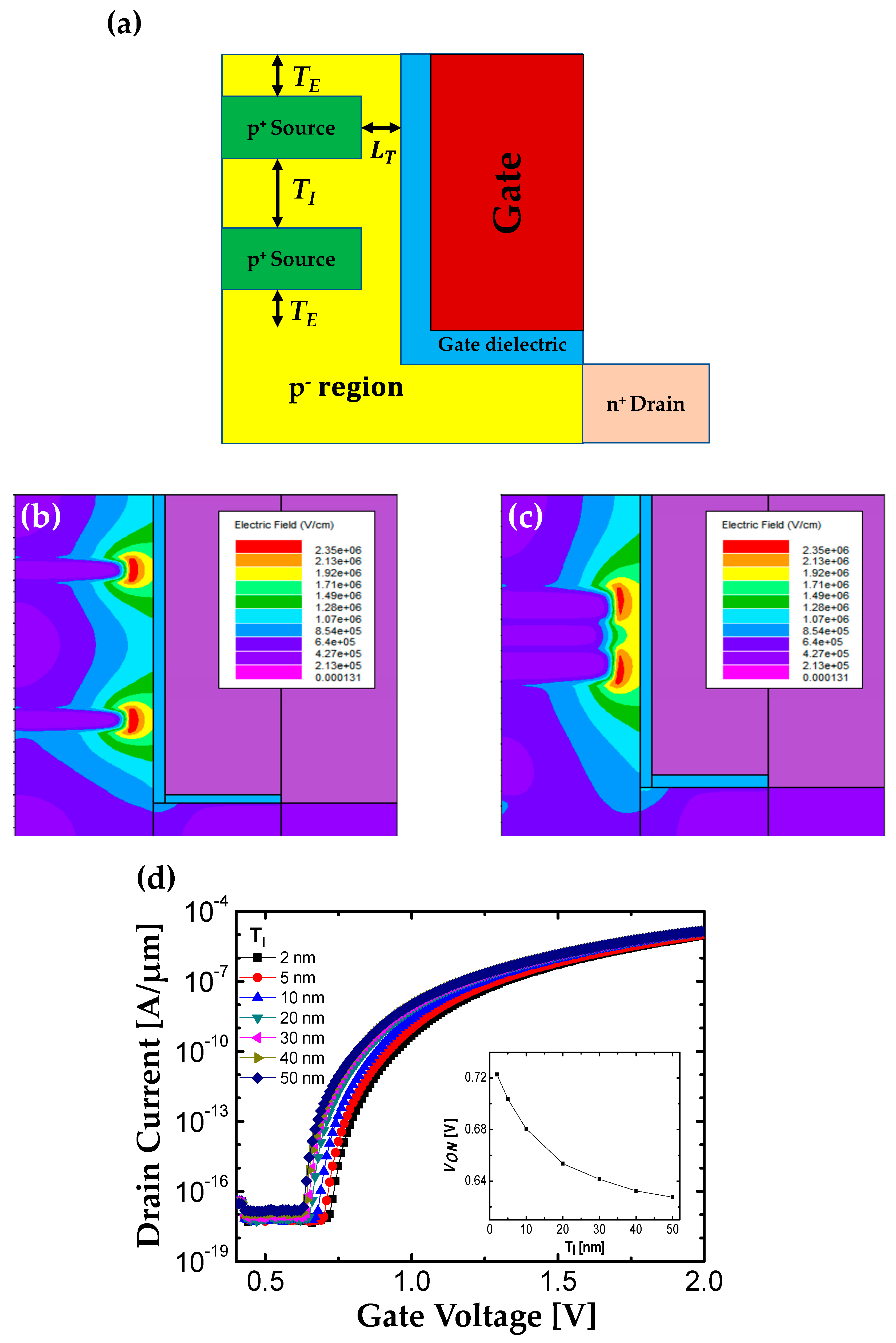
In Section 2, the parameters (TS, LT, TE) which can influence on the electric field crowding effect have been optimized by several simulations. Although F-shaped TFET can achieve the higher normalized ID (i.e., current density) as TS decreases, the smaller BTBT junction area is problematic in terms of total current for its real application. It can be addressed by adding an additional source (i.e., figure) as shown in Figure 5a. From the previous results in Section 2.3, it can be expected that the electrical characteristic of F-shaped TFET with multiple source regions is sensitively affected by the distance between the two sources (TI). Therefore, the influences of TI on the electrical performance of F-shaped TFET are investigated to determine an optimum TI. Figure 5b,c shows the effect of TI on the magnitude of the electric field at source-to-channel junction. If TI gets smaller, the electric field of both sources start to become merged and each electric field at tunnel junction is decreased. As a result, VON is increased as shown in Figure 5d and its inset. The result is well corresponded to the phenomena discussed in Section 2.3. Considering the process capability and the influence of TI on the electrical performance, TI is optimized as 30 nm.
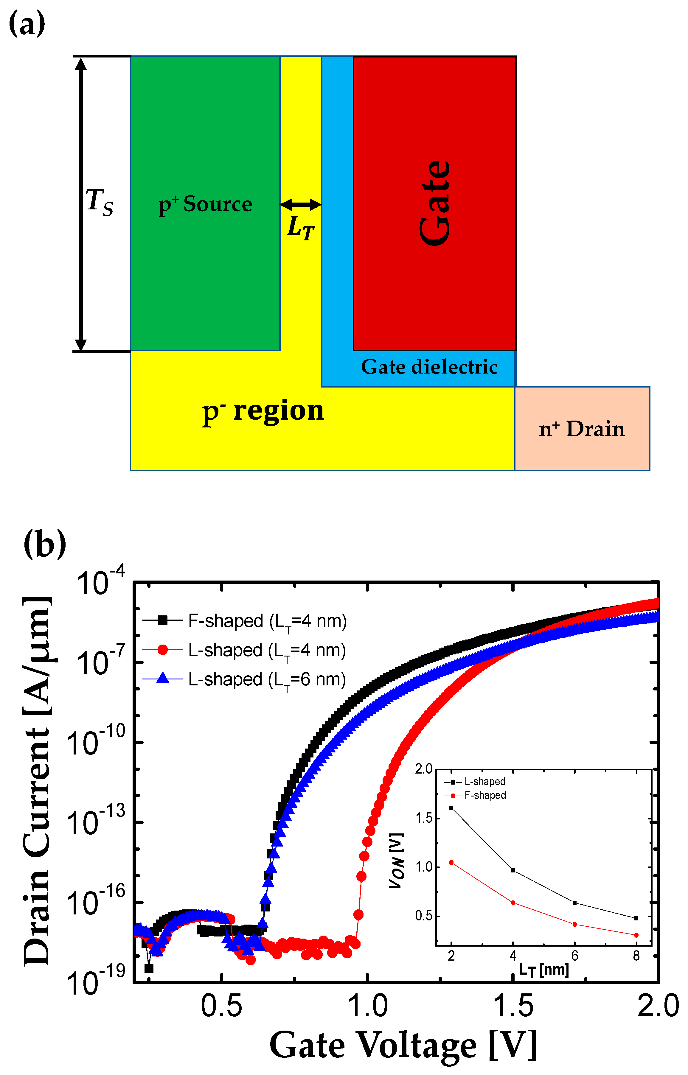
4. Comparison with L-Shaped TFET
Figure 6a shows a schematic structure of L-shaped TFET studied in [24]. Most of design parameters such as LG, TOX, NS, ND, NB, WFN and W are the same as that for the F-shaped TFET. In case of L-shaped TFET, TS is set by 70 nm which is the same as TG in optimized F-shaped TFET; TS = 5 nm, TE = 15 nm, and TI = 30 nm, TG = 2TS + 2TE + TI (Figure 5a). On the other hand, LT is set as 4 nm or 6 nm to compare with F-shaped TFET in two points of view; the same dimension or VON.
In case of 4 nm-LT, L-shaped TFET has the same dimension as the optimized F-shaped TFET discussed in Section 2.1. As shown in Figure 6b, it is clear that the VON of F-shaped TFET is about 0.4 V lower than that for L-shaped TFET in spite of the same dimension with the help of the electric field crowding effect. The inset of Figure 6b confirms that VON of F-shaped TFET is always smaller than that for L-shaped TFET with the same LT.
If the LT of L-shaped TFET is 6 nm, its VON becomes the same as that of an optimized F-shaped TFET (Figure 6b). Comparing both TFETs with the same VON, the ION, and SSAVG of F-shaped TFET are 4.8 times higher and 7 mV/dec lower than that for L-shaped TFET, respectively. The results are clearly attributed to the enhanced BTBT rate with the geometrical merits (i.e., field crowding), because F-shaped TFET has smaller BTBT junction area than L-shaped TFET.
5. Device Fabrication
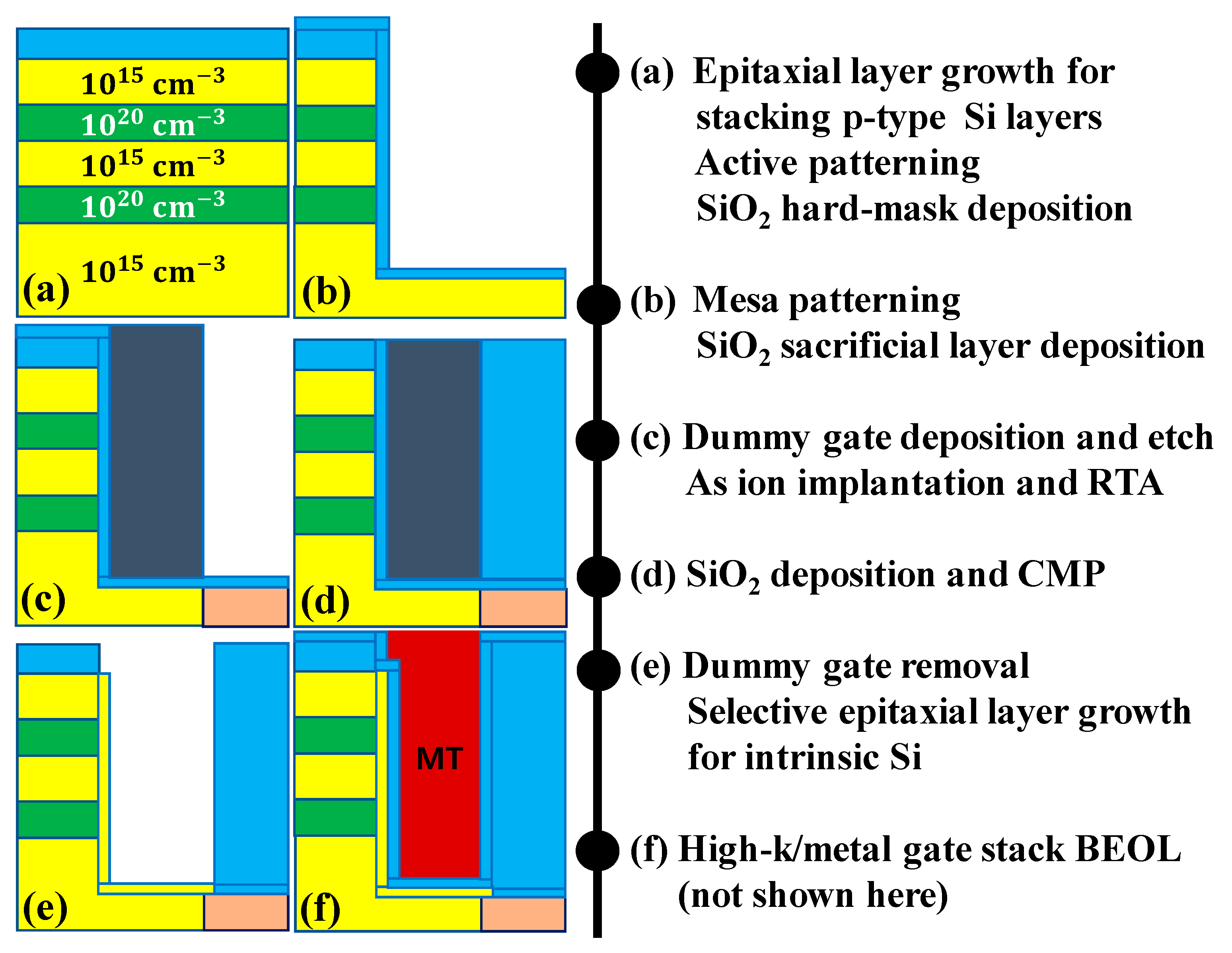
Figure 7 summarizes an exemplary self-align process flow for F-shaped TFET with multiple source regions; fingers. (Figure 7a) P-type Si layers doped by 1020 cm−3 and 1015 cm−3 are alternately stacked on Si-on-insulator (SOI) wafer through epitaxial layer growth processes. After defining an active region, SiO2 hard-mask is deposited by a chemical vapor deposition (CVD). This layer is also helpful to passivate active sidewall. (Figure 7b) Mesa patterning is followed by SiO2 buffer layer deposition. (Figure 7c) After dummy gate formation by deposition and etch-back processes, drain region is defined by arsenic (As) ion implantation and rapid thermal annealing (RTA). (Figure 7d) SiO2 deposition is followed by chemical-mechanical polishing (CMP) to expose the dummy gate. (Figure 7e) After selectively removing the dummy gate and SiO2 buffer layer, selective epitaxial layer growth (SEG) is performed to form ultra-thin tunnel region. (Figure 7f) The gate stack is formed by high-k/metal gate atomic layer deposition (ALD) processes. The back-end-of-line process is not shown here.
6. Summary
A novel F-shaped TFET is proposed and its device physics and operating mechanisms are studied in detail by using two-dimensional TCAD simulations. The results confirm that it can achieve a relatively lower VON (~0.6 V) than that for L-shaped TFET (~1.0 V) with the same LT. In addition, the current drivability of F-shaped TFET can be further improved by adding additional sources (fingers). Last of all, F-shaped TFET is expected to be fabricated by self-aligned processes. Therefore, F-shaped TFET can be regarded as one of the promising candidates for low-power digital logic applications.
Author Contributions
Conceptualization, Y.K., J.H.K., G.K. and S.K. (Sangwan Kim); Data curation, S.Y., J.O. and S.K. (Seokjung Kang); Formal analysis, S.Y. and J.O.; Investigation, S.Y., J.O. and S.K. (Seokjung Kang); Methodology, S.Y., J.O., S.K. (Seokjung Kang) and S.K. (Sangwan Kim); Supervision, S.K. (Sangwan Kim); Writing—original draft, S.Y., J.O. and S.K. (Seokjung Kang); Writing—review & editing, Y.K., J.H.K., G.K. and S.K. (Sangwan Kim).
Funding
This research was supported in part by the Brain Korea 21 Plus Project, in part by the MOTIE/KSRC under Grant 10080575 (Future Semiconductor Device Technology Development Program), in part by the NRF of Korea funded by the MSIT (Ministry of Science and ICT) under Grant NRF-2019M3F3A1A03079739 and NRF-2019M3F3A1A02072091 (Intelligent Semiconductor Technology Development Program) and in part by the MSIT (Ministry of Science and ICT), Korea, under the ITRC (Information Technology Research Center) support program (IITP-2019-2016-0-00309) supervised by the IITP (Institute for Information & communications Technology Planning & Evaluation).
Conflicts of Interest
The authors declare no conflict of interest.
References
- Wang, P.F.; Hilsenbeck, K.; Nirschl, T.; Oswald, M.; Stepper, C.; Weis, M.; Schmitt-Landsiedel, D.; Hansch, W. Complementary tunneling transistor for low power application. Solid State Electron. 2004, 4, 2281–2286. [Google Scholar] [CrossRef]
- Ionescu, A.M.; Riel, H. Tunnel field-effect transistors as energy efficient electronic switches. Nature 2011, 479, 329–337. [Google Scholar] [CrossRef] [PubMed]
- Gnani, E.; Gnudi, A.; Reggiani, S.; Baccarani, G. Drain-conductance optimization in nanowire TFETs by means of a physics-based analytical model. Solid State Electron. 2013, 84, 96–102. [Google Scholar] [CrossRef]
- Choi, W.Y.; Park, B.G.; Lee, J.D.; Liu, T.J.K. Tunneling field-effect transistors (TFETs) with subthreshold swing (SS) less than 60 mV/dec. IEEE Electron Device Lett. 2007, 28, 743–745. [Google Scholar] [CrossRef]
- Huang, Q.; Huang, R.; Zhan, Z.; Qiu, Y.; Jiang, W.; Wu, C.; Wang, Y. A novel Si tunnel FET with 36 mV/dec subthreshold slope based on junction depleted-modulation through striped gate configuration. In Proceedings of the 2012 IEEE International Electron Devices Meeting, San Francisco, CA, USA, 10–12 December 2012; pp. 187–190. [Google Scholar]
- Avci, U.E.; Morris, D.H.; Young, I.A. Tunnel field-effect transistors: Prospects and challenges. IEEE J. Electron. Devices Soc. 2015, 3, 88–95. [Google Scholar] [CrossRef]
- Ilatikhameneh, H.; Klimeck, G.; Appenzeller, J.; Rahman, R. Design rules for high performance tunnel transistors from 2-D materials. IEEE J. Electron Devices Soc. 2016, 4, 260–265. [Google Scholar] [CrossRef]
- Villalon, A.; Carval, G.L.; Martinie, S.; Royer, C.L.; Jaud, M.A.; Cristoloveanu, S. Further insights in TFET operation. IEEE Trans. Electron Devices 2014, 61, 2893–2898. [Google Scholar] [CrossRef]
- Toh, E.H.; Wang, G.H.; Chan, L.; Sylvester, D.; Heng, C.H.; Samudra, G.S.; Yeo, Y.C. Device design and scalability of a double-gate tunneling field-effect transistor with silicon-germanium source. Jpn. J. Appl. Phys. 2008, 47, 2593–2597. [Google Scholar] [CrossRef]
- Conzatti, F.; Pala, M.G.; Esseni, D.; Bano, E.; Selmi, L. Strain-induced performance improvements in InAs nanowire tunnel FETs. IEEE Trans. Electron Devices 2012, 59, 2085–2092. [Google Scholar] [CrossRef]
- Fahad, H.M.; Hussain, M.M. High-performance silicon nanotube tunneling FET for ultralow-power logic applications. IEEE Trans. Electron Devices 2013, 60, 1034–1039. [Google Scholar] [CrossRef]
- Imenabadi, R.M.; Saremi, M.; Vandenberghe, W.G. A novel PNPN-like Z-shaped tunnel field-effect transistor with improved ambipolar behavior and RF performance. IEEE Trans. Electron Devices 2017, 64, 4752–4758. [Google Scholar] [CrossRef]
- Choi, W.Y.; Lee, W. Hetero-gate-dielectric tunneling field-effect transistors. IEEE Trans. Electron Devices 2010, 57, 2317–2319. [Google Scholar] [CrossRef]
- Richter, S.; Sandow, C.; Nichau, A.; Trellenkamp, S.; Schmidt, M.; Luptak, R.; Bourdelle, K.K.; Zhao, Q.T.; Mantl, S. Ω-gated silicon and strained silicon nanowire array tunneling FETs. IEEE Electron Device Lett. 2012, 33, 1535–1537. [Google Scholar] [CrossRef]
- Cao, W.; Yao, C.J.; Jiao, G.F.; Huang, D.; Yu, H.Y.; Li, M.F. Improvement in reliability of tunneling field-effect transistor with p-n-i-n structure. IEEE Trans. Electron Devices 2011, 58, 2122–2126. [Google Scholar] [CrossRef]
- Abdi, D.B.; Kumar, M.J. In-built N+ pocket p-n-p-n tunnel field-effect transistor. IEEE Electron Device Lett. 2014, 35, 1170–1172. [Google Scholar] [CrossRef]
- Kao, K.H.; Verhulst, A.S.; Vandenberghe, W.G.; Soree, B.; Magnus, W.; Leonelli, D.; Groesenken, G.; De Meyer, K. Optimization of gate-on-source-only tunnel FETs with counter-doped pockets. IEEE Trans. Electron Devices 2012, 59, 2070–2077. [Google Scholar] [CrossRef]
- Mallik, A.; Chattopadhyay, A.; Guin, S.; Karmakar, A. Impact of a spacer-drain overlap on the characteristics of a silicon tunnel field-effect transistor based on vertical tunneling. IEEE Trans. Electron Devices 2013, 60, 935–942. [Google Scholar] [CrossRef]
- Anghel, C.; Chilagani, P.; Amara, A.; Vladimirescu, A. Tunnel field effect transistor with increased on current, low-k spacer and high-k dielectric. Appl. Phys. Lett. 2010, 96, 122104. [Google Scholar] [CrossRef]
- Kim, S.W.; Kim, J.H.; Liu, T.J.K.; Choi, W.Y.; Park, B.G. Demonstration of L-shaped tunnel field-effect transistors. IEEE Trans. Electron Devices 2016, 63, 1774–1778. [Google Scholar] [CrossRef]
- Avci, U.E.; Rios, R.; Kuhn, K.; Young, I.A. Comparison of performance, switching energy and process variations for the TFET and MOSFET in logic. In Proceedings of the 2011 Symposium on VLSI Technology-Digest of Technikal Papers, Kyoto, Japan, 14–16 June 2011; pp. 124–125. [Google Scholar]
- Senale-Rodriguez, B.; Lu, Y.; Pay, P.; Jena, D.; Seabaugh, A.; Xing, H.; Barboni, L.; Silveira, F. Perspectives of TFETs for low power analog ICs. In Proceedings of the 2012 IEEE Subthreshold Microelectronics Conference (SubVT), Waltham, MA, USA, 9–10 October 2012; pp. 1–3. [Google Scholar]
- ATLAS. User’s Manual; SILVACO International: Santa Clara, CA, USA, 2009. [Google Scholar]
- Kim, S.W.; Choi, W.Y.; Sun, M.C.; Kim, H.W.; Park, B.G. Design guideline of Si-based L-shaped tunneling field-effect transistors. Jpn. J. Appl. Phys. 2012, 51, 06FE09-1–06FE09-4. [Google Scholar] [CrossRef]
- Fossum, J.G.; Yang, J.W.; Trivedi, V.P. Suppression of corner effects in triple-gate MOSFETs. IEEE Electron Device Lett. 2003, 24, 745–747. [Google Scholar] [CrossRef]
Figure 1.
(a) Structure of the F-shaped tunnel field-effect transistor (TFET) with multiple sources. (b) Structure and parameter definitions of the F-shaped TFET.
Figure 1.
(a) Structure of the F-shaped tunnel field-effect transistor (TFET) with multiple sources. (b) Structure and parameter definitions of the F-shaped TFET.

Figure 2.
Log scale transfer characteristics with various LT at 0.7 V-drain voltage (VDS). The inset figure shows turn-on voltage (VON) and average SS (SSAVG) which is extracted by measuring SS from VON to VON + 0.7 V.
Figure 2.
Log scale transfer characteristics with various LT at 0.7 V-drain voltage (VDS). The inset figure shows turn-on voltage (VON) and average SS (SSAVG) which is extracted by measuring SS from VON to VON + 0.7 V.

Figure 3.
(a) Normalized log scale transfer characteristics with various TS at VDS = 0.7 V. The inset figure shows VON and normalized on-state current (ION) which is defined as ID at VGS = 0.5 + VON divided by TS. Electric field contour plots for (b) TS = 40 nm, (c) TS = 15 nm, (d) TS = 10 nm, (e) TS = 7.5 nm, and (f) TS = 5 nm. These plots are extracted at VDS = 0.7 V and VGS = 0.86 V which is corresponded to the VON of TS = 40 nm. (g) Schematic circuit model for F-shaped TFET.

Figure 4.
Transfer characteristic with the various TE at VDS = 0.7 V. The inset figure shows extracted VON with the variation of TE ranging from 5 to 30 nm.
Figure 4.
Transfer characteristic with the various TE at VDS = 0.7 V. The inset figure shows extracted VON with the variation of TE ranging from 5 to 30 nm.

Figure 5.
(a) Structure of F-shaped TFET with multiple sources. Electric field contour plots for (b) TI = 30 nm and for (c) TI = 5 nm at VDS = 0.7 V, VGS = 0.86 V. (d) Transfer characteristic as TI increases from 2 to 50 nm at VDS = 0.7 V. The inset figure shows extracted VON.
Figure 5.
(a) Structure of F-shaped TFET with multiple sources. Electric field contour plots for (b) TI = 30 nm and for (c) TI = 5 nm at VDS = 0.7 V, VGS = 0.86 V. (d) Transfer characteristic as TI increases from 2 to 50 nm at VDS = 0.7 V. The inset figure shows extracted VON.

Figure 6.
(a) Structure of L-shaped TFET. (b) Transfer characteristics of L-shaped and F-shaped TFETs at VDS = 0.7 V. The inset figure shows VON of both TFETs as a function of LT from 2 to 8 nm.
Figure 6.
(a) Structure of L-shaped TFET. (b) Transfer characteristics of L-shaped and F-shaped TFETs at VDS = 0.7 V. The inset figure shows VON of both TFETs as a function of LT from 2 to 8 nm.

Figure 7.
An exemplary process flow for the fabrication of an F-shaped TFET.


Table 1.
Parameters used for the technology computer-aided design (TCAD) simulation.
| Abbreviations | Parameter | Value |
|---|---|---|
| LG | Gate length | 20 nm |
| LT | Lateral length of tunnel region | Variable |
| TOX | Gate oxide thickness | 2 nm |
| TG | Gate thickness | 2TE + TS |
| TE | Space above and below source | Variable |
| TS | Source thickness | Variable |
| NS | P-type source doping concentration | 1020 cm−3 |
| ND | N-type drain doping concentration | 1018 cm−3 |
| NB | P-type body doping concentration | 1015 cm−3 |
| WFN | Gate work function | 4.05 eV |
| W | Channel width | 1 μm |
© 2019 by the authors. Licensee MDPI, Basel, Switzerland. This article is an open access article distributed under the terms and conditions of the Creative Commons Attribution (CC BY) license (http://creativecommons.org/licenses/by/4.0/).
Share and Cite
MDPI and ACS Style
Yun, S.; Oh, J.; Kang, S.; Kim, Y.; Kim, J.H.; Kim, G.; Kim, S. F-Shaped Tunnel Field-Effect Transistor (TFET) for the Low-Power Application. Micromachines 2019, 10, 760. https://doi.org/10.3390/mi10110760
AMA Style
Yun S, Oh J, Kang S, Kim Y, Kim JH, Kim G, Kim S. F-Shaped Tunnel Field-Effect Transistor (TFET) for the Low-Power Application. Micromachines. 2019; 10(11):760. https://doi.org/10.3390/mi10110760
Chicago/Turabian StyleYun, Seunghyun, Jeongmin Oh, Seokjung Kang, Yoon Kim, Jang Hyun Kim, Garam Kim, and Sangwan Kim. 2019. "F-Shaped Tunnel Field-Effect Transistor (TFET) for the Low-Power Application" Micromachines 10, no. 11: 760. https://doi.org/10.3390/mi10110760
Note that from the first issue of 2016, this journal uses article numbers instead of page numbers. See further details here.