

Abstract
The electronic structure change after plasma exposure in representative materials used in electronic devices — crystalline Si substrate and Si3N4 film — is investigated by a first-principles approach. We prepared the starting structures of Si, α-, and β-Si3N4 with various key species (Ar, Br, Cl, N, and O) in processing plasmas. We investigated the electron charge density distribution and density of state (DOS) with the interstitial species after optimizing the prepared initial structures. Model predictions showed that the interstitial species create the DOSs, and that the energy-band edge extends to the midgap. The creation of the DOSs was clearly found in the β-Si3N4 structure model, while no obvious creation was obtained in the α-Si3N4 structure. This creation of the DOSs is consistent with the current–voltage (I–V) characteristics of the damaged Si3N4 films presumably consisting of α- or β-Si3N4 local structure. The distortion of the I–V curves was considered to be attributed to the creation of the DOSs, which play a role as carrier trapping/detrapping sites.
Export citation and abstract BibTeX RIS
1. Introduction
With the aggressive shrinkage of device feature sizes in accordance with Moore's law of ultra large-scale integration (ULSI) circuits,1–8) defect creation in materials during plasma processing — plasma-induced damage (PID) — has been one of the critical issues in designing present-day electronic devices.9–11) PID induces not only the topological feature change12–16) but also the degradation of electrical performance such as the reliability17–22) in dielectric materials (SiO2, Si3N4, and low-k films)23–26) and semiconductor materials (Si).27–29) For example, plasma-induced physical damage (PPD) induced by high-energy ion bombardment is known to generate the local defect structures such as vacancies and interstitials.10) Regarding Si3N4, there are several representative local structures, namely, α-, β-, and γ-Si3N4.30) In the leading-edge process technologies, the Si3N4 films with α- and β-Si3N4 are widely used.31–34) The time-dependent creations of defective structures in Si substrates and Si3N4 films have been extensively studied.35,36) The generation of these structures is one of the critical issues in the development of high-performance ULSI circuits. Tremendous efforts have been devoted to the clarification of such defective structures by means of simulations, e.g., classical molecular dynamics (MD) simulations.11,37) However, MD simulations cannot precisely reveal the electronic structure change since it employs classical mechanics. The electronic structure change directly leads to the performance degradation of advanced electronic devices. First-principles simulations employing quantum mechanics are widely used alternative approaches to calculate the behavior of electrons, which, in particular, governs the properties of electronic structure in materials. Various studies using a first-principles simulation have been reported for understanding the electronic structure change at the reacting surface and interface of materials and the chemical reactions in a plasma bulk.38–41) However, there have been few reports focusing on the detailed local electronic structure change (defect creation) particularly induced by incoming species from the present-day processing plasmas. In this work, we performed a first-principles approach based on the density functional theory (DFT)42–44) to investigate the effects of defect creation in the Si substrate and Si3N4 film on the performance of devices. Key species in the present-day processing plasmas, i.e., Ar, Br, Cl, N, and O, were inserted in the original structures in the simulations. The creation of the local electron charge density and density of state (DOS) was investigated. The impacts on the electronic structures are discussed in detail with respect to the inserted species.
2. Plasma-induced physical damage in various materials
The schematic of PID in the Si substrate and Si3N4 film is shown in Fig. 1. In general, PID is categorized into three types on the basis of the mechanism of its generation: (a) physical damage, (b) charging damage, and (c) radiation damage. Figure 1 illustrates these mechanisms during plasma processes for various materials such as the Si substrate and Si3N4 film. Physical damage is induced by high-energy ion bombardment on material surfaces.45) Charging damage is induced by conduction current J from plasma flowing into dielectric materials.20) Radiation damage is induced by high-energy photon interactions.46,47) All of the PID mechanisms lead to the generation of "latent defects" in materials, by way of the interaction of the bonding network with incident ions, conducting electrons, and incoming high-energy photons. The defective structures result in the destructive change in the electronic structures. The resultant electronic structures behave as carrier trapping/detrapping sites and degrade the electrical performance of devices. In this study, we focus on PPD that deforms the local structures by incident ions (species) in widely used materials such as Si and Si3N4.
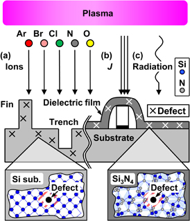
Fig. 1. Illustrations of various PID creation mechanisms in Si substrate and Si3N4 films: (a) physical damage, (b) charging damage, and (c) radiation damage.
Download figure:
Standard image High-resolution image3. Simulation scheme
3.1. Calculation method
All DFT calculations were performed using the projector augmented-wave (PAW) method48) as implemented in the plane-wave PWscf code in Quantum-Espresso package.49,50) The Perdew–Burke–Ernzerhof (PBE) exchange–correlation functional51) was applied. The kinetic energy cut-off values for wave functions and that for local electron charge density were 50 and 200 Ry, respectively. The k-point meshes of the Brillouin zone for primitive cells were sampled with 4 × 4 × 4 (unless otherwise noted) on the basis of the Monkhorst–Pack scheme.52) Periodic boundary condition was employed. In the DFT calculations, one solves the Kohn–Sham (KS) equation:43)

where  , N is the number of electrons, ħ is the Dirac's constant, m is the electron mass, and Veff is the effective potential. Ei and ψi are the KS eigenvalues and the eigenwave functions, respectively. One can determine the local electron charge density ρ(r) with respect to the wave functions:
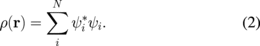
Figure 2 shows a flowchart of the present DFT scheme. Firstly, we set the initial structures by defining the atomic position ri and the number Zi. Secondly, the effective potential (Veff) was calculated by assuming the initial electron charge density, and then the KS equation was solved as the diagonalization problem by using Veff. The electron charge density ρ(r) was evaluated from the KS equation. The numerical procedure was continued with the latest ρ(r) until the convergence criterion was satisfied (Δρ(r) < ε). ε is the parameter for the convergence tests. When the criterion was satisfied, i.e., the self-consistency was achieved in the present scheme, the final electron charge density ρout(r) along with the total energy of the system, Etotal, was calculated. Note that the initial structure prepared for the simulations (Si, α-, and β-Si3N4) was determined from the ρout(r) value defining the minimum value of Etotal. The same procedure was performed also for the optimization of the damaged structures studied in this work. On the basis of the obtained ρout(r), one can predict the DOS.
Fig. 2. Flowchart of the DFT calculation scheme employed in this study.
Download figure:
Standard image High-resolution image3.2. Starting structures
We prepared the initial structures for Si, α-, and β-Si3N4. The Si crystalline unit structure was obtained from the space group  configuration.53) The α- and β-Si3N4 unit structures were obtained from the space group P31c and P63/m (hexagonal) configurations, respectively.54,55) The lattice constants and the internal atomic positions were completely optimized in accordance with the procedure mentioned in Sect. 3.1. Note that Si3N4 films have two respective local structures, i.e., α- and β-Si3N4, as shown in Figs. 3(a) and 3(b), respectively.56) In the typical Si3N4 film, the tetrahedral SiN4 structures are the common unit and they are linked with each other at N atoms to form the amorphous network. After constructing the initial structure based on the present scheme, we inserted various species in the prepared cells. Figure 4 shows the schematic illustrations of the starting structures with the interstitial species being introduced for (a) Si, (b) α-, and (c) β-Si3N4. The visualization models were constructed using VESTA.57) We denote these structures as PPD structures, which will be investigated in the following sections. Figures 4(b) and 4(c) show the top and side views of the local structures (α- and β-Si3N4, respectively). We inserted one interstitial atom as an incoming atom from plasma, i.e., Ar, Br, Cl, N, and O, at various positions into the initial structures. The interstitials are shown as white spheres in Fig. 4. We simulated PPD in Si and Si3N4 films by using the present first-principles calculations. DOS was derived from the electron charge density distribution. The DOS implies the effects of PPD on the electrical performance of damaged devices. To further confirm the DOS of the Si network, we constructed a (3 × 1 × 1) supercell of Si unit cells and inserted one interstitial in each supercell. With respect to the supercell of Si, the k-point meshes of 3 × 9 × 9 were employed for carrying out the Brillouin zone integration.

Fig. 3. Ideal unit structures of (a) α-Si3N4 and (b) β-Si3N4. Si atoms are in blue (dark) and N atoms are in gray.
Download figure:
Standard image High-resolution image
Fig. 4. Unit structures of (a) Si, (b) α-Si3N4, and (c) β-Si3N4. The upper panels in (b) and (c) are the top views and the lower panels are the side views for (b) α-Si3N4 and (c) β-Si3N4, respectively. Si atoms are in blue (dark) and N atoms are in gray. The white spheres indicate the interstitial: Ar, Br, Cl, N, or O.
Download figure:
Standard image High-resolution image4. Results and discussion
4.1. PPD to Si
Figure 5 shows the unit structure and the electron charge density ρ(r) of (a) the ideal crystalline Si and (b) the damaged Si structure with an inserted Br atom. In the damaged Si structure, Si–Si bonds were weakened and additional electron distributions were observed around the interstitials. We found that the hexagonal site is stable for Ar, Br, Cl, and N atoms, while the bond-centered site is stable for an O atom. The electronic structure change was investigated in terms of DOS (carrier traps) as shown in Fig. 6. In the calculations, the (3 × 1 × 1) supercell was used. The band gap of the ideal Si was calculated as 0.48 eV, which is widely discussed as the band gap problem.58) As can be seen, the interstitial atoms (Ar, Br, Cl, N, and O) create the respective DOSs and the energy-band edge extends to the midgap.
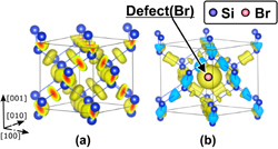
Fig. 5. Unit structure and electron charge density ρ(r) of (a) ideal crystalline Si and (b) damaged Si structure with an inserted Br atom as shown in pink (dark).
Download figure:
Standard image High-resolution image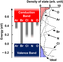
Fig. 6. DOS of Si in damaged structures with various interstitials. The gray areas indicate the created local DOS. The detailed DOSs are shown on the right panel.
Download figure:
Standard image High-resolution image4.2. PPD to α- and β-Si3N4
Figure 7 shows examples of the unit structure and the electron charge density ρ(r) of the damaged (a) α- and (b) β-Si3N4 structures with an inserted Br atom. It was found that Si–Si and Si–N bonds were weakened in both structures and electron trap sites were created around the interstitial atoms (Ar, Br, Cl, N, and O). The electronic structure change was investigated in terms of DOS as shown in Figs. 8(a) and 8(b). In Fig. 8, the gray areas indicate the local DOS distributions and the solid lines indicate the average energy of defect sites. The band gaps of the ideal α- and β-Si3N4 were calculated as 4.6 and 4.4 eV, respectively. In the case of α-Si3N4, the local DOS emerged near the valence band in the Br-, Cl-, and N-damaged models and near the conduction bands in the Br-, N-, and O-damaged models. No isolated DOS was found in the Ar-damage model. In the case of β-Si3N4, the local DOS emerged near the conduction band in the Ar-, Br-, Cl-, and N-damaged models, and near the midgap in the Br-, Cl-, and O-damaged models. As seen in Fig. 8, the difference in the energy level of defect was revealed.
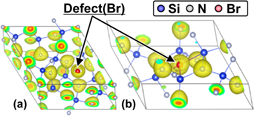
Fig. 7. Unit structure and electron charge density ρ(r) of (a) α- and (b) β-Si3N4 damaged structures with an inserted Br atom as shown in pink (dark).
Download figure:
Standard image High-resolution image
Fig. 8. DOSs of (a) α-Si3N4 and (b) β-Si3N4 in damaged structures with various interstitials. The gray areas indicate the created local DOS and the solid lines, the average energy level of the created DOS.
Download figure:
Standard image High-resolution image5. Comparison with experiments
5.1. Sample structure and plasma experiment
The creation of DOS predicted by first-principles calculations was compared with experimental data. An Si3N4 film formed on a 12 in. p-type Si(100) substrate was used as a dielectric film and exposed to Ar plasma under various bias powers. Since this Si3N4 film was formed by a conventional method, the local structure of the film can be α-, β-Si3N4, or their mixture.56) The initial thickness of the Si3N4 film was determined to be approximately 106 nm by scanning electron microscopy (SEM) analysis. The operating pressure was 2.7 Pa. The ion flux was adjusted to be approximately constant by controlling the ICP source power, and was determined to be 1.0 × 1015 cm−2·s−1 by using a Langmuir probe. The exposure time was 60 s. The ion dose was estimated as 6.0 × 1014 cm−2. A 400 kHz bias was applied to a sample stage. The bias power was varied to control the dc self-bias voltage (|Vdc| ∼ incident ion energy) from −200 to −950 V determined using an oscilloscope. The details of the plasma treatment are reported elsewhere.59)
The electrical characteristic change due to the plasma exposure was identified by a current–voltage (I–V) measurement. The relationship between applied voltage and leakage current was monitored using a mercury (Hg) probe system. The damaged structure is assumed to be a pseudo-MOS structure. In the evaluation of I–V characteristics, one believes that the creation of trap sites and the SiO2/Si interface state results in the distortion of I–V curves.
5.2. Prepared cell structure and simulation results
As mentioned in Sect. 4.2, the creation of the DOSs was clearly found in the β-Si3N4 structure model. Therefore, we focused on DOS creation in the respective β-Si3N4 structure to clarify the root cause of the shift and distortion of the I–V curves. In addition to the model prediction shown in Fig. 8, we constructed a larger cell, i.e., (1 × 1 × 3) supercell of β-Si3N4 to investigate the effects of DOS creation on the I–V curves. The electronic structure change was determined by the procedure mentioned in Sect. 3. The k-point meshes were set to 6 × 6 × 4 for the Brillouin zone integration. Figure 9 shows the DOS for β-Si3N4 units using the larger cell. The black thick and red thin solid lines indicate the DOSs of the ideal and Ar-damage structures of β-Si3N4, respectively. The black dashed and dotted lines indicate the DOSs of the Br- and Cl-damage structures, respectively. As seen in Fig. 9, the energy-band edge extends to the midgap, and the interstitial species (Ar, Br, and Cl) create the local DOSs in the energy gap, whose energy level depends on the inserted species. In the case of the Ar-damage model, the local DOS emerged near the conduction band. The local DOS also emerged near the conduction band and the midgap in both the Br- and Cl-damage models. Below, we focus on the effects of the DOS on I–V curves for Ar-damage cases.

Fig. 9. Detailed DOSs of the ideal and damaged β-Si3N4 structures with Ar, Br, and Cl interstitials. The black thick solid line indicates the DOS of the ideal crystalline β-Si3N4. The red (dark) thin solid line corresponds to the DOS of the damaged β-Si3N4 model with the Ar interstitial. The black dashed and dotted lines indicate the DOS of the damaged β-Si3N4 model with the Br and Cl interstitials, respectively. Ev and Ec are the energies at the top of the valence band and the bottom of the conduction band for the ideal crystalline β-Si3N4, respectively.
Download figure:
Standard image High-resolution image5.3. Discussion on I–V characteristics
Figure 10 illustrates the schematics of energy band structures in an Si3N4 film. Figure 10(a) shows the equilibrium energy band structure. Figures 10(b) and 10(c) show the energy bands under low and high bias voltages, respectively. In the low-bias-voltage region, the key role that the defect plays is to shorten the tunneling distance by the creation of electron hopping sites (DOSs) as shown in Fig. 10(b). In other words, these hopping sites assist the electron tunneling, leading to an increase in the leakage current (Ileak). On the other hand, in the high-bias-voltage region, the key role that the defect plays is to induce the electrostatic potential change by trapped electrons as shown in Fig. 10(c). This leads to the extension of tunneling distance for conducting electrons injected from the metal electrode. Although the leakage current increases as the bias voltage increases, the potential change extends the tunneling distance, resulting in a decrease in the leakage current compared with the unexposed samples. Owing to these captured electrons, the conduction band edge of Si3N4 increases. Figure 11 shows the I–V curves of the damaged samples after Ar plasma exposure under various Vdc conditions. Previous reports using MD simulations11) suggested that the principal structures created in the deeper region of the Si substrate consist of primarily interstitial and dumbbell Si, instead of vacancies.60) Thus, we presume that the shift and distortion of the I–V curves are owing to the creation of these respective structures by PID. As seen in Fig. 10, the leakage current was found to increase in a low-bias-voltage region and decrease in a high-bias-voltage region, which was predicted by the present simulations. It is anticipated that the distortion of the I–V curves agrees well with the model predictions. The present results suggest that the interstitial species — PPD — create the gap state acting as a carrier trapping/detrapping site and distort the leakage current characteristics, which should be carefully taken into account in designing the performance of devices with Si3N4 films.
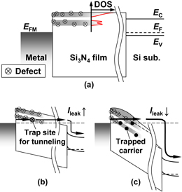
Fig. 10. Schematic of the energy band diagrams in an Si3N4 film under (a) equilibrium, (b) a low bias stress, and (b) a high bias stress. EFM is the Fermi level for the metal. Ev, Ec, and EF are the energies at the top of the valence band, the bottom of the conduction band, and the Fermi level for the Si substrate, respectively.
Download figure:
Standard image High-resolution image
Fig. 11. I–V characteristics of the unexposed (Ref.) and damaged Si3N4 films. The samples were exposed to Ar plasmas under various Vdc conditions.
Download figure:
Standard image High-resolution image
6. Conclusions
The electronic structure change induced by plasma processing was predicted on the basis of the DFT calculations by introducing various etch species, namely, Ar, Br, Cl, N, and O, into the Si, α-, and β-Si3N4 structures. We found that the interstitials (Ar, Br, Cl, N, and O) create the local DOS and change the electronic structures of the materials. The present results suggest that the created DOS may play a role as a carrier trapping/detrapping site. Model prediction was verified by the experimental I–V measurements. From the calculated DOS, one can predict the shift and distortion of the I–V curves (a leakage current increase) caused by PID, which degrades the performance and reliability of devices. The first-principles approach performed in this study is a useful method for the analysis of the electrical performance degradation of plasma-damaged devices.
Acknowledgements
The authors would like to thank Mr. T. Ikeda of Tokyo Electron Technology Solutions for this support, and Mr. T. Kuyama of Kyoto University for the I–V measurement. This work was financially supported by Grants-in-Aid for Scientific Research (15H04159 and 16K14405) from the Japan Society for the Promotion of Science.