

Abstract
The ferromagnetic (FM)/antiferromagnetic (AF) bilayer structures have drawn intensive attention because of their wide applications in modern spintronic devices. While abundant published works have been reported on the interface effects of the FM/AF bilayers caused by the magnetic field annealing (MFA) process, the volume effects caused by the MFA treatment have been rarely considered. In this work, the microstructural and magnetic properties of the NiO/CoFe bilayers with various CoFe thicknesses were investigated under different annealing temperatures. At high annealing temperature, the interlayer mixing and exchange coupling between NiO and CoFe layers were promoted and consequently the interface effects were facilitated. The interfacial oxides acted as pinning centers and randomly pinned the FM domains, leading to an increase of coercivity and a considerable degradation of uniaxial anisotropy. The increase of coercivity was also contributed by the enhancement of the interfacial exchange coupling between the NiO and CoFe layers after MFA. As the CoFe thickness increased, the volume effects tended to dominate over the interface effects, resulting in the preservation the uniaxially anisotropic features of CoFe. These results indicate that both the coercivity and anisotropic features of the NiO/CoFe bilayers can be directly affected by the MFA process, opening up the possibility of modifying the magnetism in the NiO/CoFe bilayers and offering an effective way to improve the performance of modern spintronic devices.
Export citation and abstract BibTeX RIS
1. Introduction
The ferromagnetic (FM)/antiferromagnetic (AF) bilayer structures have been widely investigated because understanding their mechanism is crucial for their applications in modern spintronic devices.1,2) The microstructural and magnetic properties of the FM/AF bilayers can be altered by many techniques, such as magnetic field annealing (MFA),3,4) ion-beam bombardment,5,6) field cooling,7) and so on. Among these techniques, the MFA treatment is an effective way to modify the microstructure of the bilayers, including crystallographic orientations,8) grain sizes,9) interlayer mixing,10,11) etc. The modified microstructure induced by MFA can be categorized into two groups: 1) changes of interfacial properties (interface effects) and 2) changes of microstructural properties in FM and AF thin films (volume effects). Abundant published works have been reported on the interface effects of the FM/AF bilayers caused by the MFA process.4,10,12–21) An extended interfacial region in metal/NiO systems after annealing was exhibited due to the chemical reaction and diffusion at the interface.10) The interface features are closely related to the interface spin configuration and thus have a considerable impact on the magnetic properties of the FM/AF bilayers.13) However, the volume effects caused by the MFA treatment have been rarely considered, and therefore it has been investigated in this work.
The AF NiO was selected due to its high Neel temperature and great corrosion resistance. The microstructural and magnetic properties of the CoFe/NiO bilayers were investigated with different annealing temperatures (TMFA = 523, 573, and 623 K). The CoFe thickness (20, 30, and 40 nm) was tuned to study both the microstructural interface and volume effects on the magnetism of the CoFe/NiO bilayers.
2. Experimental methods
The NiO/CoFe bilayers were prepared on amorphous SiO2 substrates by using a dual ion-beam sputtering deposition technique.22) The base pressure of the chamber was 4 × 10⁻⁵ Pa (3 × 10⁻⁷ Torr). A Kaufman ion source (800 V, 7.5 mA) was used to focus an Ar ion-beam onto a commercial Co90Fe10 (at. %) target surface in order to deposit the bottom CoFe layer. To deposit the top NiO layer, an End-Hall ion source (VEH = 70 V, 500 mA) with a mixture of O2 and Ar (16% O2/Ar) was used to in-situ bombard the substrate and to oxidize the Ni layer. The working pressure of the chamber was maintained at 6.67 × 10⁻² Pa (5 × 10⁻⁴ Torr) and no magnetic field was applied during deposition. The NiO/CoFe bilayers with NiO thickness of 25 nm and CoFe thickness of 20, 30, and 40 nm were prepared. For the annealed samples, post-deposition MFA processes were carried out under high vacuum (1 × 10⁻⁷ Torr, 1.33 × 10⁻⁵ Pa) with a 500 mT (5000 Oe) magnetic field applied parallel to the film plane. The samples were annealed for one hour at different temperatures (TMFA = 523, 573, and 623 K). The lower limit of the MFA temperature range was set to 523 K (nearly equal to the Neel temperature of NiO) to establish the AF ordering of NiO as well as to minimize the microstructural and compositional changes caused by the MFA treatment. To avoid significant interlayer mixing and prevent the formation of NiO/CoFe nanocomposite, the upper limit of the MFA temperature range in this work was set to 623 K. A JEOL JIB-4601 focused ion beam (FIB) operating at 30 kV was used to prepare the cross-sectional samples and a JEOL JEM-2010 transmission electron microscope (TEM) operating at 200 kV was used for the microstructural analysis. X-ray diffraction (XRD) patterns were acquired using a Bruker AXS D8 Advance (incident angle of 0.4°). Magnetic hysteresis loop measurements were performed in a commercial MicroSense DMS vibrating sample magnetometer (VSM) at room temperature.
3. Results and discussion
Microstructural properties of the NiO/CoFe bilayers were characterized by TEM. Figures 1(a) and 1(b) show the bright-field TEM images of the as-deposited and annealed NiO (25 nm)/CoFe (20 nm) bilayers, which exhibit a slight increase of the grain sizes after the MFA process at 623 K. The growth of grains can also be observed in the inserted cross-sectional TEM images [inset of Fig. 1(b)], where the relatively large light-colored regions are revealed. Compared to the clear interfaces in the as-deposited NiO/CoFe bilayer [inset of Fig. 1(a)], the rough interfaces in the annealed bilayer [inset of Fig. 1(b)] indicates that the MFA process caused the interlayer mixing at the NiO/CoFe and CoFe/SiO2 interfaces. To acquire more microstructural information, the selected area electron diffraction (SAED) patterns of the as-deposited and annealed bilayers were investigated, as shown in Figs. 1(c) and 1(d). The NiO layer exhibits a cubic rock-salt structure10) while the CoFe layer shows a hcp structure.23) For the as-deposited bilayers [Fig. 1(c)], the NiO layer mainly exhibits textures (200) and (111) while the CoFe layer shows a combination of textures (002), (110), and (004). However, the diffraction ring of the CoFe(002) texture seems to be overlapped by that of the NiO(200) texture. The crystallographic properties of the CoFe layer were further studied with XRD spectra (discussed below). After MFA [Fig. 1(d)], the diffraction ring corresponding to the NiO(200) texture became dominant and the diffraction rings corresponding to other textures became dimmer, suggesting the preferred orientation of the NiO was changed to (200) after annealing. Furthermore, abundant bright diffraction spots were identified in the NiO(200) and CoFe(002), (101) textures for the annealed bilayers [Fig. 1(d)], which indicated the growth of grains in the annealed bilayers. These results are in agreement with the observation of enlarged grains in the TEM images for the annealed samples [Fig. 1(b)]. During the MFA process, the interlayer mixing at the NiO/CoFe and CoFe/SiO2 interfaces also resulted in the formation of oxide phases such as Co3O4 or Fe3O4, as shown in the SAED patterns for the annealed samples [Fig. 1(d)].

Fig. 1. TEM micrographs of (a) as-deposited and (b) annealed (TMFA = 623 K) NiO (25 nm)/CoFe (20 nm) bilayers. Cross-sectional TEM images are shown in the insets of (a) and (b). SAED patterns indexed with different orientations of the as-deposited and annealed bilayers are shown in (c) and (d), respectively.
Download figure:
Standard image High-resolution imageXRD measurements were performed to further study the effects of the MFA treatment on the crystallographic properties of the NiO (25 nm)/CoFe (20 nm) bilayers, as shown in Figs. 2(a) and 2(b). In the as-deposited bilayers [Fig. 2(a)], the peak intensities of the NiO(111) and (200) textures are much larger than those of other textures NiO(220) and (311). The CoFe layer exhibits a dominant CoFe(002) texture. After the MFA process, the NiO(200) texture became dominant, as revealed by the largest peak intensity of the NiO(200) in Fig. 2(b). These phenomena are a result of the reordering of preferred orientation of the NiO crystallites during the MFA process and are consistent with the previously discussed SAED patterns [Figs. 1(c) and 1(d)]. For the CoFe layer [Fig. 2(b)], the peaks from the CoFe(002) and (101) textures are observable. Also, the stronger peaks from NiO and CoFe layers in the annealed samples [Fig. 2(b)] indicate the improvement of crystallinity and the growth of grains caused by the MFA treatment, which is in agreement with the observed SAED patterns as well. The peaks from the interfacial oxides (e.g., Co3O4 or Fe3O4) are not observed in the annealed samples [Fig. 2(b)], because the grain sizes of these alloyed phases are too small to produce observable peaks in the XRD spectra, as suggested by the dim diffraction spots shown in the SAED patterns [Fig. 1(d)]. For the as-deposited bilayers [Fig. 2(a)], while the calculated lattice constants (a ∼ 2.53 Å, c ∼ 4.01 Å) of the hcp CoFe are close to those of the bulk (a ∼ 2.50 Å, c ∼ 4.06 Å), the lattice constant (a ∼ 4.26 Å) of the rock-salt NiO determined from the XRD patterns is slightly expanded, as compared to that of the bulk (a ∼ 4.18 Å). After the MFA treatment at 623 K [Fig. 2(b)], the lattice constants were determined to be a ∼ 4.22 Å for NiO and a ∼ 2.51 Å, c ∼ 4.07 Å for CoFe. The lattice constants for both NiO and CoFe became closer to their bulk values, which suggests that microstructural relaxations occurred in both the NiO and CoFe layers during the MFA process. Our results show that the MFA treatment can notably alter the microstructure and composition of the NiO/CoFe bilayers by facilitating the growth of grains, causing the interlayer mixing, forming the interfacial oxide phases, reordering of the preferred crystallographic orientations, and promoting microstructural relaxations.

Download figure:
Standard image High-resolution image
Fig. 2. XRD spectra of (a) as-deposited and (b) annealed (TMFA = 623 K) NiO (25 nm)/CoFe (20 nm) bilayers.
Download figure:
Standard image High-resolution imageTo investigate the influence of the MFA process on the magnetic properties of the NiO/CoFe bilayers, VSM measurements were carried out on both the as-deposited and annealed thin films, as shown in Fig. 3. Compared to the as-deposited NiO/CoFe (40 nm) bilayer (μ0Hc ∼ 1 mT, remanence Mr/Ms ∼ 0.95), the annealed NiO/CoFe (∼40 nm) bilayer [TMFA = 523 K, Fig. 3(a)] exhibited a similar μ0Hc but a higher remanence (Mr/Ms ∼ 1) when the measuring field was applied along the in-plane easy axis (parallel configuration, 0°). However, when the in-plane measuring field direction was rotated away from the easy axis, the remanence decreased to ∼0.7 at 45° and finally dropped to ∼0.1 at 90° (transverse configuration), as shown in Fig. 3(a). Due to the MFA treatment, the magnetocrystalline anisotropies of the CoFe grains were aligned along the in-plane easy axis, resulting in the observed uniaxially anisotropic features. This induced uniaxial anisotropy gave rise to the shift from an in-plane easy axis (parallel configuration, 0°) to an in-plane hard axis (transverse configuration, 90°) magnetization, as exhibited in Fig. 3(a).
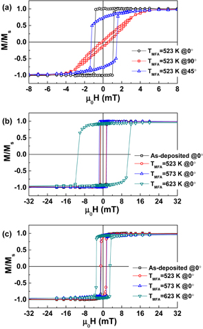
Fig. 3. (a) In-plane angular dependence of hysteresis loops of a NiO (25 nm)/CoFe (40 nm) bilayer measured at 0° (parallel configuration), 45°, and 90° (transverse configuration). Hysteresis loops of (b) NiO (25 nm)/CoFe (20 nm) bilayers and (c) NiO (25 nm)/CoFe (30 nm) bilayers annealed at different temperatures (TMFA = 523, 573, and 623 K).
Download figure:
Standard image High-resolution imageHysteresis loops of the NiO/CoFe bilayers annealed at different temperatures (TMFA = 523, 573, and 623 K) were characterized at room temperature at the parallel configuration (0°), as shown in Figs. 3(b) and 3(c). Compared to the as-deposited NiO (25 nm)/CoFe (20 nm) bilayers, the annealed bilayers (TMFA = 523 K) exhibit almost the same magnitude of coercivity (μ0Hc ∼ 1 mT), as shown in Fig. 3(b). When the annealing temperature was increased to 573 K, a slight growth of coercivity (μ0Hc ∼ 1.8 mT) was identified, which was contributed by the enhancement of exchange coupling between the NiO and CoFe layers after MFA or the pinning sites created by the interlayer mixing during the MFA process. The Co and Fe oxides formed at the NiO/CoFe and CoFe/SiO2 interfaces could induce magnetic inhomogeneities and act as pinning sites. Further increasing the annealing temperature to 623 K [Fig. 3(b)], a significantly boosted coercivity (μ0Hc ∼ 11 mT) was exhibited in the annealed bilayers with the CoFe thickness of 20 nm, indicating that the stronger FM/AF exchange coupling was probably enabled. Also, for the bilayers annealed at high temperature (TMFA = 623 K), the interlayer mixing at the NiO/CoFe and CoFe/SiO2 interfaces was remarkably promoted, giving rise to the formation of more interfacial oxide phases (e.g., Co3O4 or Fe3O4), as demonstrated in the TEM images [Fig. 1(d)]. These interfacial oxides acted as pinning centers and hindered the domain-wall motion during the magnetization reversal process, which resulted in a further increase of the coercivity. The alloys forming among Ni, Fe, and Co could probably induce pinning centers as well, although they were not clearly identified in the SAED and XRD results. A notably increased coercivity (μ0Hc ∼ 3.5 mT) was also identified in the annealed (TMFA = 623 K) bilayers with the CoFe thickness of 30 nm, as shown in Fig. 3(c). The enhancement of the coercivity in the annealed NiO (25 nm)/CoFe (30 nm) bilayers was less significant than that of the NiO (25 nm)/CoFe (20 nm) bilayers. As the thickness of the CoFe layer increased, the volume effects became dominant over the interface effects and the domains farther away from the interfaces were less affected by the interfacial pinning centers or interfacial exchange coupling, which gave rise to the relatively small coercivity of the annealed bilayers with a thicker CoFe layer. When the annealing temperature was reduced to 573 K, less interfacial oxides were formed and thus the pinning effects from the interfacial pinning centers (e.g., Co3O4 or Fe3O4) were trivial in the NiO (25 nm)/CoFe (30 nm) bilayers. Therefore, at the annealing temperature of 573 K, while only a slight increase of the coercivity (μ0Hc ∼ 1.8 mT) was exhibited in the NiO (25 nm)/CoFe (20 nm) bilayers [Fig. 3(b)], no noticeable change in coercivity was revealed in the NiO (25 nm)/CoFe (30 nm) bilayers [Fig. 3(c)]. These results reveal that the MFA process can alter the coercivity of the NiO/CoFe bilayers by facilitating the formation of interfacial pinning centers or establishing interfacial exchange coupling. As the CoFe thickness increased, the volume effects dominated over the interface effects.
The hysteresis loops for both the NiO (25 nm)/CoFe (20 nm) and NiO (25 nm)/CoFe (30 nm) bilayers were further characterized with the in-plane measuring magnetic field applied along the easy axis (parallel configuration, 0°) and hard axis (transverse configuration, 90°), as shown in Fig. 4. At the annealing temperature of 573 K [Figs. 4(a) and 4(b)], both the NiO (25 nm)/CoFe (20 nm) and NiO (25 nm)/CoFe (30 nm) bilayers exhibited the uniaxially anisotropic behavior of the CoFe layer. These results are in line with the above argument that the pinning effects were trivial at the relatively low annealing temperature (TMFA = 573 K) and the volume effects played a dominant role. Only a small amount of pinning sites were formed at 573 K, which therefore resulted in the trivial pinning effects and the preservation of the uniaxially anisotropic features of CoFe. As the annealing temperature increased to 623 K [Figs. 4(c) and 4(d)], the remanence (Mr/Ms) values (at transverse configuration, 90°) revealed a remarkable increase for both the NiO (25 nm)/CoFe (20 nm) and NiO (25 nm)/CoFe (30 nm) bilayers, indicating that the uniaxially anisotropic CoFe crystallites were disordered to a great extent. When the annealing temperature was boosted up to 623 K, the interlayer mixing was greatly facilitated and more interfacial pinning sites were formed. The CoFe domains were randomly pinned by these pinning sites, leading to a considerable degradation of the uniaxial anisotropy. For the NiO (25 nm)/CoFe (30 nm) bilayers [Fig. 4(d)], a highly asymmetric hysteresis loop was exhibited when the in-plane measuring magnetic field was applied transversely (90°), as shown in Fig. 4(d). The rounded descending branch suggests that the rotation of the interfacial magnetizations played a major role in the magnetization reversal process,9,24) while the approximately rectangular ascending branch indicates the domain wall motion was dominant.25) This statement is further supported by the rounded descending and ascending branches revealed in the hysteresis loop for the NiO (25 nm)/CoFe (20 nm) bilayers measured at the in-plane transverse configuration [90°, Fig. 4(c)], where the influence of the interface effects was considerable and thus the rotation of the interfacial magnetizations became more dominant in the magnetization reversal process. These results demonstrate that the anisotropy properties of the NiO/CoFe bilayers can also be modified due to the competition between the interface and volume effects caused by the MFA process.

Download figure:
Standard image High-resolution image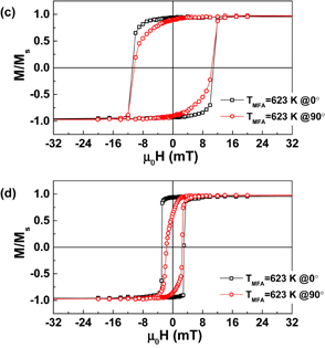
Fig. 4. Hysteresis loops of NiO (25 nm)/CoFe (20 nm) bilayers measured at parallel (0°) and transverse (90°) configurations with annealing temperature of (a) TMFA = 573 K and (c) TMFA = 623 K. Hysteresis loops of NiO (25 nm)/CoFe (30 nm) bilayers measured at parallel (0°) and transverse (90°) configurations with annealing temperature of (b) TMFA = 573 K and (d) TMFA = 623 K.
Download figure:
Standard image High-resolution image
4. Conclusions
In this work, the influence of the post-deposition magnetic field annealing (MFA) process on the microstructural and magnetic properties of the NiO/CoFe bilayers was investigated. The MFA treatment could notably alter the microstructure and composition of the NiO/CoFe bilayers by facilitating the growth of grains, causing the interlayer mixing, forming the interfacial oxide phases, reordering of the preferred crystallographic orientations, and promoting microstructural relaxations. At high annealing temperature, the promotion of the interlayer mixing and consequently the facilitation of the interface effects could remarkably alter the coercivity and anisotropy of the NiO/CoFe bilayers. The enhancement of the coercivity was contributed by the increase of exchange coupling between the NiO and CoFe layers after MFA or the pinning sites created by the interlayer mixing during the MFA process. The interfacial oxides acted as pinning centers and hindered the domain-wall motion during the magnetization reversal process, which resulted in a further increase of the coercivity. The FM domains were randomly pinned by these interfacial pinning sites, leading to a considerable degradation of the uniaxial anisotropy. Compared to the bilayers with a relatively thin CoFe layer, the volume effects played a more significant role in the bilayers with a thicker CoFe layer. As the CoFe thickness increased, the volume effects became dominating over the interface effects, resulting in the preservation of the uniaxially anisotropic features of CoFe. These results indicate that both the coercivity and anisotropic features of the NiO/CoFe bilayers can be directly affected by the MFA process, opening up the possibility of modifying the magnetism in the NiO/CoFe bilayers and offering an effective way to improve the performance of modern spintronic devices.
Acknowledgements
This work was supported in part by the MOST of Taiwan, the NSERC and CFI of Canada, and the Seed Funding Program for Basic Research and Small Project Funding Program from the University of Hong Kong, ITF Tier 3 funding (ITS/104/13, ITS/214/14), and University Grants Committee of Hong Kong (Contract No. AoE/P-04/08).