
Abstract
Utilizing spintronics-based nonvolatile memories in integrated circuits offers a promising approach to realize ultralow-power and high-performance electronics. While two-terminal devices with spin-transfer torque switching have been extensively developed nowadays, there has been a growing interest in devices with a three-terminal structure. Of primary importance for applications is the efficient manipulation of magnetization, corresponding to information writing, in nanoscale devices. Here we review the studies of current-induced domain wall motion and spin–orbit torque-induced switching, which can be applied to the write operation of nanoscale three-terminal spintronics devices. For domain wall motion, the size dependence of device properties down to less than 20 nm will be shown and the underlying mechanism behind the results will be discussed. For spin–orbit torque-induced switching, factors governing the threshold current density and strategies to reduce it will be discussed. A proof-of-concept demonstration of artificial intelligence using an analog spin–orbit torque device will also be reviewed.
Export citation and abstract BibTeX RIS
1. Introduction
The continued progress of electronics achieved in the past half century has mainly been based on the miniaturization of semiconductor devices, which has followed Moore's law.1) While the engineering of such devices to meet the requirements of ICs has become increasingly difficult as the technology node has been scaled down, alternative pathways, generally referred to as "More than Moore", have been recognized as promising candidates, where new-concept devices that can facilitate further advances in ICs are employed. Among them, spintronics is recognized to offer attractive approaches as it provides nonvolatile memories with virtually unlimited endurance and a high-speed operation capability.2) By replacing volatile working memories such as static random access memories (SRAMs) and dynamic random access memories (DRAMs) by nonvolatile spintronics-based ones, i.e., magnetoresistive random access memories (MRAMs), one can drastically reduce the power consumption of ICs while maintaining high performance as was demonstrated in recent studies.3–8) Spintronics memory devices can be classified into two categories according to their structure: two- and three-terminal devices. Both devices generally include a magnetic tunnel junction (MTJ), and the read operation is performed using the tunnel magnetoresistance (TMR) effect.9–16) On the other hand, various schemes can be used for the write operation. Spin-transfer torque (STT)-induced magnetization switching17–23) is the most common scheme of the write operation for two-terminal devices, and MRAMs with STT switching, so-called STT-MRAMs, have been developed by several groups.4,7,24–26) Owing to a number of successive breakthroughs,16,27–31) STT-MRAMs are now close to practical use. Electric-field-induced magnetization switching32,33) is another option for the write operation of two-terminal devices. Since the energy consumption via Joule heating can be greatly reduced,34) intensive research has also been actively performed in recent years on this front. Meanwhile, for three-terminal devices, which are the main focus of this article, current-induced magnetic domain wall (DW) motion35–40) or spin–orbit torque (SOT)-induced magnetization switching41–43) can be used for their write operation (classical Oersted field-induced magnetization switching44,45) and STT-induced switching46,47) can also be used, although we will not discuss them here). As discussed in detail later, three-terminal devices achieve high operation speed and high reliability at the cost of the footprint, making them an attractive replacement for high-speed memories such as SRAMs. Three-terminal DW-motion MRAMs48,49) and a microcontroller unit with a SOT-device-based MRAM6) have been demonstrated to date.
In the following sections, we will first describe the characteristics of the three-terminal cell structure from the viewpoint of the circuit and give an overview of current-induced DW motion and SOT-induced switching (Sect. 2). Next, we will show our recent studies on the DW motion and SOT-induced switching in nanoscale devices in Sects. 3 and 4, respectively, which were carried out with the aim of replacing volatile working memories. In Sect. 4, we will also present a demonstration of associative memory operation using an artificial neural network with a SOT device, which is expected to open a new horizon of spintronics and artificial intelligence. Finally, a conclusion will be given in Sect. 5.
2. Three-terminal spintronics devices
In this section, we will first describe the characteristics of three-terminal spintronics devices. It will be followed by an explanation of the basic principles of current-induced DW motion and SOT switching and a review of several key studies.
2.1. Structure and characteristics of three-terminal spintronics device
Figure 1 shows a schematic of the typical structure of a three-terminal spintronics device with a cell circuit. The unit cell consists of two transistors and one MTJ device, namely a 2T1MTJ structure.50) A word line is connected to the gate of the transistors and two write bit lines are connected to the source/drain. The other source/drain is connected to the recording part of the MTJ device. A reference layer with a fixed magnetization is placed on top of the recording part via a tunnel barrier, and its top terminal is connected to a read bit line or a ground line. For a DW-motion device the recording part consists of a magnetic wire containing a single DW and information is encoded by the position of the DW. Meanwhile, a SOT device consists of a heterostructure with a heavy-metal channel and a magnetic free layer; information is encoded by the direction of the magnetization of the free layer. The cell size for the smallest layout is 12–18F2 (F denotes the feature size of the MTJ layer), which is larger than the two-terminal counterpart (6F2) but much smaller than that of SRAMs (>100F2).51) The write current is applied through the recording part and the read current is applied through the MTJ, as shown by the broken arrows in Fig. 1. The separation of the current paths used for reading and writing allows high-speed and reliable (in terms of both soft and hard errors) operation and a simple and small-area peripheral circuit, which is described in detail in Ref. 52. Consequently, in contrast to the two-terminal counterpart, in which 2T2MTJ,53) 4T2MTJ,4) and 6T2MTJ54,55) cell structures are used to achieve the high-speed random access required to replace SRAMs, the three-terminal device achieves it with the 2T1MTJ structure, allowing a small cell size and low dynamic power consumption. It is also noted that a two-port SRAM function can be realized by a 5T2MTJ structure50) and a relatively large capacity can be achieved by a 9T8MTJ structure.56) In addition, a nonvolatile flip-flop with a toggle frequency of 3.5 GHz has been developed with a three-terminal device, where its design flexibility was utilized.57)
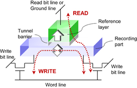
Fig. 1. Structure of three-terminal spintronics memory cell consisting of two transistors and one MTJ device.
Download figure:
Standard image High-resolution image2.2. Current-induced DW motion
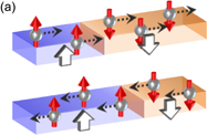
Current-induced DW motion, depicted in Fig. 2(a), takes place as a result of the s–d exchange interaction and the conservation of angular momentum. To be specific, the change in the angular momentum of electrons that pass through a DW is adiabatically transferred to the localized magnetization, resulting in DW motion along the electron flow. This phenomenon was initially predicted by Berger in 198435) and has been experimentally observed since 2004.36–38) The torque generated in this regime is referred to as the adiabatic STT.58–60) The threshold current density Jth for the DW motion observed in most of the earlier studies,37–40) however, was significantly smaller than that expected from the adiabatic STT model, except for in studies on the diluted magnetic semiconductor (Ga,Mn)As with a perpendicular easy axis,36) which was well explained by a corresponding model.61) Thus, the theory was developed to include a nonadiabatic STT, the so-called β term, to explain the experimental observation.62–64) Since the β term has the same symmetry as the magnetic field, unlike the adiabatic STT, Jth is proportional to the critical field HC as was later experimentally confirmed.65) This means that there is a trade-off between the high thermal stability of stored information and a small driving current for non-adiabatic STT-induced DW motion. In this regard, the adiabatic regime is more suitable for application. Subsequently, it was theoretically predicted that by using perpendicular-easy-axis systems with a reduced wire thickness, the hard-axis anisotropy, which governs Jth in the adiabatic regime becomes so small that a DW can be moved by the adiabatic STT at a reasonably small current density.66,67) Following the theoretical prediction, experimental studies using a perpendicular-easy-axis Co/Ni multilayer demonstrated DW motion driven with a small current density,68–71) as explained well by the adiabatic-STT model.71) In this system, the independence between Jth and HC was also confirmed.72,73) Also note that, although not described in detail in this article, chiral Néel walls stabilized by the Dzyaloshinskii–Moriya interaction74–76) in perpendicular-easy-axis heterostructure systems can be moved by SOT77–79) and high-speed motion of up to 750 m/s was demonstrated.80) However, the torque acting in this regime again has the same symmetry as the field, leading to a linear relationship between HC and Jth.81)
Download figure:
Standard image High-resolution image
Fig. 2. Schematics of write techniques for three-terminal spintronics device. (a) Current-induced DW motion. (b) SOT-induced magnetization switching.
Download figure:
Standard image High-resolution image2.3. SOT-induced magnetization switching
SOT is generated via spin–orbit interactions when a current is applied to systems with broken inversion symmetries. SOT-induced magnetization switching was first observed in a (Ga,Mn)As thin film with noncentrosymmetry.82) The switching in a heavy-metal/ferromagnet heterostructure was first reported in a Pt/Co/AlOx system by Miron et al. in 2011.41) In such heterostructure systems, applying in-plane current to the heavy-metal channel gives rise to the accumulation of spin-polarized electrons in the ferromagnetic layer, which generate the SOT acting on the magnetization and switch it, as shown in Fig. 2(b). It was found that SOT has two vector components, namely Slonczewski-like torque and field-like torque.83,84) The origin of SOT in heterostructures is still controversial in spite of a number of intensive experimental85–92) and theoretical93–96) studies. One of the most likely mechanisms that account for SOT is the spin Hall effect,97–103) whose strength is generally characterized by the spin Hall angle θSH. An equally important constituent of SOT is the Rashba–Edelstein, or inverse spin-galvanic, effect.104,105) Theoretical studies revealed that both the spin Hall and Rashba–Edelstein effects exhibit Slonczewski-like and field-like torques,93–96) making it difficult to identify the origin of SOT in employed systems. Moreover, recent theoretical and experimental studies have pointed out that the transparency at the heavy metal/ferromagnet interface106–108) and the spin Hall effect localized at the interface109–111) also affect the resultant SOT. In view of these circumstances, we use the "effective" spin Hall angle  as a parameter to quantify the strength of SOT in this article. The switching scheme based on SOT can be classified into the following three categories in terms of the magnetic-easy-axis direction with respect to the channel: a perpendicular-easy-axis scheme that achieves switching under an in-plane field along the channel direction;41) an in-plane scheme with the easy axis orthogonal to the channel that achieves switching without fields;42) and an in-plane scheme with the easy axis collinear to the channel that achieves switching under a perpendicular field.43) Whereas the switching mechanism of the second scheme is basically the same as that of the well-understood STT switching, there are several issues requiring more study for the first and third schemes, for example, the factors governing Jth and the dynamics in ns and sub-ns timescales.112–114) Our studies addressing Jth will be described later. Regarding the materials that can be used for the channel layer, switching has been observed with nonmagnetic Pt,41) Ta,42) W,115) Hf,116) Ir-doped Cu,117) antiferromagnetic PtMn,118) IrMn,119) and the topological insulator BiSbTe.120) Another attractive system for SOT-induced switching is antiferromagnetic CuMnAs, where a staggered SOT originating from the inverse spin-galvanic effect acts on the antiferromagnetically aligned moments accommodated in two sublattices.121)
3. Current-induced DW motion
From now on, we will review our studies on current-induced DW motion followed by those on SOT-induced switching, which were carried out with the aim of application to three-terminal devices. To replace leading-edge volatile working memories, the properties at reduced dimensions are of particular interest. We thus studied the DW-motion and SOT-induced switching properties as a function of the device size in the nanometer region. First, we will describe the studies on DW motion.52,122–124)
3.1. Size dependence of device properties
As described in the previous section, a Co/Ni multilayer with a perpendicular easy axis has been found to be a promising material system for achieving adiabatic-STT-driven DW motion. For practical use, a small critical current, typically less than 100–200 µA, and a short time, typically less than 1–2 ns, required to displace a DW between two pinning sites, are necessary for the replacement of SRAMs. The thermal stability factor, Δ ≡ E/kBT, should be greater than 60–80 to ensure 10 years' retention, where E is the energy barrier, kB the Boltzmann constant, and T the absolute temperature.
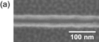
The stack structure employed here was, from the substrate side, Ta(3)/Pt(2)/[Co(0.3)/Ni(0.6)]N/Co(0.3)/Pt(1.5)/Ta(3) (thickness in nm). The stacking number N of the Co/Ni bilayer was varied from 2 to 6, corresponding to magnetic layer thickness tmag from 2.1 to 5.7 nm. The films were deposited on a high-resistivity Si wafer by dc magnetron sputtering. Magnetization hysteresis loop measurement using a vibrating sample magnetometer revealed that the spontaneous magnetization MS and effective anisotropy energy density Keff varied from 0.97 to 0.94 T and 0.26 to 0.14 MJ/m3, respectively, as N was varied from 2 to 6. The deposited films were patterned into nanowires with a pair of Hall probes by using electron beam lithography and Ar ion milling. The nominal width of the wire W was varied from 20 to 240 nm. Figure 3(a) shows a scanning electron micrograph of the patterned wire with a nominal width of 20 nm. The actual wire width determined electrically from the wire resistance was found to be close to the nominal value; for example, the former was 19.9 nm for the latter of 20 nm. The device structure used to measure the DW-motion properties is depicted in Fig. 3(b) with the measurement setup. To inject a DW into the magnetic wire, a current pulse generating an Oersted field was applied to a Cr/Au electrode (Oersted line, hereafter), which was prepared in the orthogonal direction to the DW conduit. The anomalous Hall effect was used to examine the DW motion. Evaluation of the critical current IC and Δ started from the state where a DW was initialized on the leftside of the Hall cross, whereas the DW-motion velocity vDW was evaluated from the state where a DW is injected in the vicinity of the Oersted line (see Ref. 52 for the detailed procedure of the measurement). Δ was quantified by analyzing the external field dependence of the characteristic depinning time, which was determined by fitting the Néel–Brown model to multiple depinning-measurement data.73) All the measurements were conducted at room temperature.
Download figure:
Standard image High-resolution image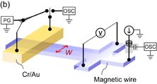
Fig. 3. (a) Scanning electron micrograph of fabricated magnetic wire with a nominal width of 20 nm. (b) Device structure for measurement of current-induced DW motion with measurement circuit.
Download figure:
Standard image High-resolution imageFigures 4(a)–4(c) show the obtained IC, write time tW, and Δ as a function of device width.52) To calculate tW from vDW, the finite width of the DW, the alignment margin, and the depinning time125) were taken into consideration. Although Jth slightly varies with W71,124) as described later, IC almost linearly decreases with decreasing W [Fig. 4(a)] due to the dominant contribution of the reduced cross section of the wire. vDW was found to be almost independent of W and thus tW also scales with W [Fig. 4(b)] due to the reduced length that the DW must travel. Importantly, both IC and tW satisfy the requirements for the replacement of SRAMs when the width becomes less than around 50 nm. Meanwhile, Δ maintains a sufficient value throughout the studied range of W [Fig. 4(c)]. These results demonstrate that a small write current/time and high thermal stability can be obtained simultaneously at reduced dimensions owing to the independence between the critical current and critical field.72,73) As a consequence, the DW-motion efficiency defined by Δ/IC (µA−1) increases with decreasing W and exceeds 2 µA−1 at around 20 nm.123) This is in contrast to two-terminal STT devices, where Δ and IC scale in a similar fashion with the device size at small dimensions, leading to size-independent efficiency in the first order of approximation. Thus, the DW-motion device with the Co/Ni multilayer can be regarded as a promising candidate for the three-terminal device that can be used in future ICs with advanced technology nodes.
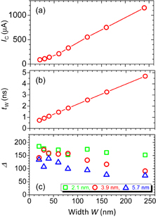
Fig. 4. Properties of DW-motion device as a function of device width W. (a) Critical current IC. (b) Write time tW. (c) Thermal stability factor Δ. Wires with N = 4 (tmag = 3.9 nm) were used for (a) and (b), and those with N = 2, 4, and 6 (tmag = 2.1, 3.9, and 5.7 nm) were used for (c). For (a) and (b), each plot represents the average value obtained from 80 devices and for (c), it is the average value from three devices.
Download figure:
Standard image High-resolution image3.2. Mechanism governing thermal stability of DW
In Fig. 4, the high Δ in the narrow region is particularly notable since, in general, Δ decreases with decreasing device size in this range of dimensions due to the volume reduction, as has been seen for two-terminal MTJ devices.126,127) Moreover, Δ appears to slightly increase as W decreases in a wider range and also it is larger for larger tmag. To understand these intriguing behaviors, we analyzed the results in more detail.123) It is known that the energy barrier E for DW depinning is given by 2MSHC0Veff,128) where HC0 is the intrinsic critical field, which was found to be inversely proportional to the wire width in our devices. Veff is the effective volume governing E. From the experimentally determined E, MS, and HC0, Veff was obtained as shown in Fig. 5 for stacks with different tmag. It starts to increase linearly with increasing W up to a certain critical width Wcrit (indicated by arrows), above which it is almost constant, as shown by the dotted lines. This result indicates that the geometrically defined volume governs E only below Wcrit, and that a portion of a DW, a subvolume, excited inside the whole DW with a length scale of Wcrit governs the value of E above Wcrit. A similar feature was observed in two-terminal MTJ devices, where the volume of the whole recording layer governs the thermal stability only below a critical size characterized by the DW width.129–131) Another intriguing feature of the result shown in Fig. 5 is that Wcrit increases as tmag decreases. In order to gain a better understanding of the underlying mechanism behind these results, we developed an analytical model in which the DW elastic energy and the Zeeman energy were taken into account. Two different shapes of the excited subvolume following the random-bond and random-field disorder models132) were considered. For both models, the existence of a subvolume and the experimentally observed tmag dependence of Wcrit were found to be qualitatively explained by considering the tmag dependence of the DW elastic energy. The findings obtained here are expected to allow us to design nonvolatile DW-motion devices.
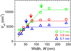
Fig. 5. Effective volume governing the thermal stability factor of a DW as a function of width W for different magnetic wire thicknesses tmag. Each plot represents the average obtained from three devices. Dotted lines are a guide to the eye and arrows indicate the critical width.
Download figure:
Standard image High-resolution image3.3. Threshold current density versus wire width
We will next show the W dependence of Jth and discuss the challenges to further miniaturize DW-motion devices.124,133) Previous studies revealed that when a DW is driven by adiabatic STT, Jth takes a minimum value at a certain width where the DW configuration transits from a Bloch wall to a Néel wall.71) Below the transition width, Jth increases with decreasing W. This fact leads to the prediction that, below a certain wire width, Jth becomes so large that one cannot apply the driving current without damaging the wire, which was found to be around 1.5 × 10¹² A/m2 for the case of a Co/Ni nanowire.134) To investigate this, we fabricated a large number of devices with various widths down to less than 20 nm and evaluate their Jth. In this study, we used a similar device structure and the same measurement circuit as that shown in Fig. 3(b), except for the stack structure of the Hall probes, which were made of a Ta/Pt underlayer only, i.e., the magnetic layer was etched (see Fig. 1 in Ref. 124). This structure enables us to more accurately examine the actual wire width dependence of Jth. The obtained value of Jth are plotted by solid symbols as a function of the electrically determined actual width in Fig. 6. In line with the previous studies,71) Jth decreases and then increases with decreasing W. At W = 30–40 nm, Jth becomes minimum. The open symbols denote values of current density below which DW motion was not observed in the device. Such devices were frequently found below around 20 nm, indicating that a DW-motion device with the present Co/Ni multilayer cannot be easily miniaturized down to less than around 20 nm. The open circles show the calculated values obtained from a micromagnetic simulation, where adiabatic STT was assumed to be the driving force of the DWs. The position of the minimum observed in the experiment was reproduced, and the inaccessibly large Jth below around 20 nm was also validated. The difference in the minimum value of Jth between the experiment and calculation can be attributed to the variation of the wire width along the longitudinal direction, that is, in the experiment, Jth should be determined by the part of the wire at which Jth becomes maximum. In the adiabatic regime, Jth is given by58–60)
where e is the elementary charge, ħ the Dirac constant, P the spin polarization of conduction electrons, ΔDW the DW width parameter, and HK⊥ the hard-axis anisotropy field. The micromagnetic simulation revealed that ΔDW is insensitive to the wire width, and hence the W dependence of Jth is mainly dominated by the W dependence of HK⊥. This fact indicates that a reasonably small Jth can be achieved at reduced dimensions by using materials having a narrow DW since the transition of the DW configuration takes place in narrower regions in such a case. In light of this insight, we further calculated the W dependence of Jth for various structural and material parameters. We found that when materials with high magnetic anisotropy, such as an L10-ordered Co-Pt alloy, are used, the transition width decreases and Jth < 1 × 10¹² A/m2 is possible even at W < 10 nm.
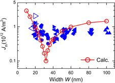
Fig. 6. Threshold current density Jth for DW motion as a function of width W. Red open circles are calculation results obtained from a micromagnetic simulation. Blue open symbols indicate that DW motion was not observed at current densities below the plots.
Download figure:
Standard image High-resolution image4. SOT-induced switching
We now turn to SOT-induced switching. We will first review the studies to clarify the factors that govern Jth for SOT switching and strategies to reduce it.135–138) Here, Ta/CoFeB/MgO and W/CoFeB/MgO structures with a perpendicular easy axis were used, which can provide high thermal stability at reduced scales. After that, we will describe an analog-like switching behavior observed in an antiferromagnetic PtMn and ferromagnetic Co/Ni heterostructure system,118) and show a proof-of-concept demonstration of artificial intelligence operation utilizing the system.139)
4.1. Factors governing threshold current density in nanoscale devices
As explained in Sect. 2.3, SOT has two vector components. Among them, the field-like component has the same symmetry as the magnetic field along the y-direction (the x- and z-axes are taken along the channel and film normal directions, respectively), which cannot alone induce the reversal of perpendicular magnetization. On the other hand, the effective field of Slonczewski-like torque has rotational symmetry with the form of  , where m denotes the unit vector of magnetization. Therefore, it can induce the reversal under the application of a static field along the x-direction (Hx), which breaks the symmetry.140) Also, in a naive picture, the spin Hall effect and Rashba–Edelstein effect give rise to the Slonczewski-like and the field-like torques, respectively. Thus, an early theoretical study gave an analytical expression for Jth by considering the Slonczewski-like torque generated by the spin Hall effect as141)
where tF is the thickness of the ferromagnetic layer and  is the effective anisotropy field. In the following, we discuss the validity of Eq. (2).
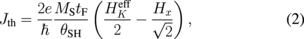
For this study, films with a stack structure of Ta(tTa)/CoFeB(1)/MgO(1.3)/Ta(1) (thickness in nm) were deposited on thermally oxidized Si substrates by dc/rf magnetron sputtering. The Ta channel layer thickness tTa was varied from 1 to 5 nm. The deposited films were patterned into Hall bar devices with a 10-µm-wide channel and a pair of Hall probes by photolithography and Ar ion milling. The processed wafers were subsequently annealed at 300 °C for 1 h. To evaluate the current-induced effective field, or SOT, a dc transport measurement was performed, where the polar angle of the external magnetic field was swept around the pole while monitoring the Hall resistance originating from the anomalous Hall effect and planar Hall effect. By rotating the field in the x–z and y–z planes, respectively, the Slonczewski-like effective field HSL and field-like effective field HFL were quantified (see Ref. 135 for more details). To evaluate the SOT-induced switching properties, the magnitude of the dc channel current was swept under the application of a static field along the x-direction (see Ref. 136 for more details). The direction of switching changed when the field direction was reversed, and the relation between the switching, current, and field directions was consistent with that expected from the switching driven by the spin Hall effect of Ta with negative θSH. All the measurements were performed at room temperature.
Figures 7(a) and 7(b) show the obtained current-induced effective fields and Jth, respectively, as a function of tTa. The effective fields are normalized by the current flowing in the whole stack. It can be seen that both the Slonczewski-like and field-like effective fields have a sizable magnitude and the latter is about twice as large as the former, which is consistent with previous studies.83,84) Also, both components have a similar dependence on tTa, implying that they have the same origin. It was also confirmed that when the effective fields are normalized by current density flowing in the Ta layer JTa, the tTa dependence of the normalized effective fields can be well fitted by the drift-diffusion model140) with a spin diffusion length of 0.5 nm, which assumes the spin Hall effect of Ta as the origin of the effective field. These results suggest that the spin current due to the spin Hall effect of Ta plays a major role in the observed effective fields. Meanwhile, Ith also has a similar tTa dependence to that of the effective field, indicating that the switching was driven by the SOT detected in the transport measurement. However, when the results of transport measurement [Fig. 7(a)] and switching [Fig. 7(b)] were compared quantitatively, a large discrepancy was found as follows. From the relation between the Slonczewski-like effective field and spin Hall angle,141)
 was obtained to be about 0.03. Then, by substituting it into Eq. (2), the expected Jth was calculated to be 1.4 × 10¹³ A/m2. On the other hand, the experimentally obtained Ith corresponds to Jth of (3–6) × 1010 A/m2, that is, they are different by a factor of 200–500.
Fig. 7. Current-induced effective fields and threshold current for switching of 10-µm-wide Hall devices. (a) Current-induced effective fields with Slonczewski-like HSL and field-like HFL symmetries per unit current I as a function of Ta channel thickness tTa. (b) Threshold current Ith at μ0Hx = 0.2 T as a function of tTa (μ0 is the permeability in free space).
Download figure:
Standard image High-resolution imageOne possible explanation for the discrepancy is that in the experiment the ferromagnetic layer does not behave as a single-domain magnet, while the theory assumes a coherent reversal. In fact, several groups have studied SOT-induced magnetization switching in the Ta/CoFeB/MgO system with different device sizes, obtaining values of Jth in the range of 1010–1012 A/m2.42,142,143) Moreover, since dc currents were used for the measurement in Fig. 7(b), Joule heating may also affect Jth, while the effect of a finite temperature is not considered in Eq. (2). Thus, to clarify the "intrinsic" factors governing Jth in nanoscale devices, we fabricated SOT switching devices with various sizes down to a single-domain scale and evaluated the switching properties using pulsed current with various durations down to 5 ns.137)
The stack structure used here was, from the substrate side, Ta(5)/CoFeB(1.2)/MgO(1.5)/Ta(1), which was deposited on a high-resistivity Si wafer by sputtering. Using electron-beam lithography and Ar ion milling, CoFeB/MgO/Ta layers were patterned into dots with various diameters D from 30 to 80 nm. A scanning electron micrograph of a dot with a nominal diameter of 30 nm is shown in Fig. 8(a). The observed diameter was found to be close to the nominal value. Figure 8(b) illustrates the fabricated device structure with the measurement circuit. A magnetic dot made of CoFeB/MgO was formed on top of a cross-shaped Ta channel, whose ends were connected to a coplanar waveguide. As a reference, a micrometer-size Hall bar device with the same geometry as that used for Fig. 7 was also fabricated on the same wafer. The magnetization reversal was examined through the anomalous Hall effect. We separately determined the thermal stability factor Δ and the effective perpendicular anisotropy field  by measuring the probability of magnetization switching induced by a pulsed perpendicular field, which were fitted by the Stoner–Wohlfarth model.144) The obtained Δ is plotted as a function of D in Fig. 8(c). As also seen in MTJ devices,127) Δ is almost constant down to a critical diameter (∼40 nm in the present case), below which it decreases. This indicates that below 40 nm, the dots should behave as a single-domain magnet, allowing us to compare the switching properties with those calculated from the macrospin model.
  was obtained to be around 0.25 T and was not virtually varied with D.
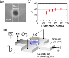
Fig. 8. (a) Scanning electron micrograph of fabricated magnetic dot with a nominal diameter D of 30 nm. (b) Device structure and measurement circuit for SOT switching experiment. (c) Thermal stability factor Δ vs D.
Download figure:
Standard image High-resolution imageFigure 9 shows the measured Jth as a function of D for different pulse durations. To induce switching, a static magnetic field of 20 mT was applied along the x-direction. One can see that Jth for the nanoscale devices is one order of magnitude larger than that of the micrometer-size Hall device (1.5 × 10¹¹ A/m2), indicating that the above-mentioned discrepancy between the experiment and theory is partly caused by spatial inhomogeneity and Joule heating, which become significant as the device scale increases. Meanwhile, Jth only slightly increases with decreasing D in the nanometer region and, more importantly, even in the single-domain-size devices, it is 3–4 times smaller than the value derived from Eq. (2) shown by the broken line.
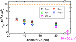
Fig. 9. Threshold current density Jth as a function of D for different pulse durations. The broken line at Jth = 1.4 × 10¹³ A/m2 indicates the value expected from the conventional theory.
Download figure:
Standard image High-resolution imageFor the reasons accounting for the remaining discrepancy in Jth between the theory based on a macrospin model and the experiment on single-domain-size devices, we considered the effects of a finite temperature and the field-like torque, which were not taken into account in the derivation of Eq. (2). To clarify the effect of these factors, we measured the switching probability under current pulse application for a 40 nm device and analyzed the data. The details are not described here, but we found that, whereas an analytical expression including the effect of a finite temperature cannot reproduce the results consistently, the results can be reasonably described by a numerical simulation based on a macrospin model including the field-like torque with magnitude twice as large as the Slonczewski-like torque. In other words, the field-like torque was found to decrease Jth for SOT switching. However, an unusually large Gilbert damping constant had to be assumed to reproduce the results here, and its reason remains as an open question.
In summary, we found that micrometer-size devices do not provide the "intrinsic" Jth for SOT switching, and even in a nanometer-size device Jth cannot be explained without considering the field-like component of SOT. Note also that the SOT-induced switching in devices with a current and magnetic-easy-axis collinear configuration can also be explained well by macrospin simulation including the field-like torque.43,145) In addition, a space-resolved magnetization reversal in perpendicular-easy-axis large patterns has been studied by several groups, revealing that the Oersted field plays a key role in domain nucleation and the Dzyaloshinskii–Moriya interaction plays a key role in DW propagation.146–151) Also, a theoretical work showed that the reduction of Jth by the field-like torque strongly depends on the sign of the field-like torque.152)
4.2. Reduction of threshold current density by tungsten
Our study on SOT switching in single-domain-scale Ta/CoFeB/MgO devices (Fig. 9) revealed that Jth is (3–4) × 1012 A/m2, which corresponds to Ith of 750–1000 µA for a three-terminal device with a channel width of 50 nm. This is too large for the replacement of SRAMs. A possible way to reduce Jth and Ith is to use W for the channel layer because a giant spin Hall angle has been experimentally reported for W.92,115,153–155) It has also been reported that the giant spin Hall effect is obtained only when the W is thin enough and forms a high-resistivity metastable β phase.115) In addition, the structure of W was reported to strongly depend on the deposition conditions.156–159) Thus, following the above studies, we investigated the SOT switching of devices with a W channel deposited under various conditions.138)
In this work, the power and gas pressure during the sputtering were changed, and the variation of the structure and resistivity of W with the deposition conditions was evaluated. From X-ray diffraction and sheet-resistance measurements, it was found that a lower sputtering power and higher gas pressure tend to promote the formation of the β phase with higher resistivity. When W was sputtered at powers of 10 and 30 W under an Ar gas pressure of 0.17 Pa, the β phase was maintained even at a thickness of 20 nm. We fabricated the SOT-switching devices depicted in Fig. 8(b) with three different deposition conditions for W: (power, pressure) = (100 W, 0.06 Pa), (100 W, 0.17 Pa), and (30 W, 0.17 Pa), and evaluated their switching properties. The stack structure used here was W(5)/CoFeB(1.3)/MgO(2)/Ta(1).
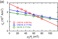
For all the devices with various deposition conditions, switching in the same direction as that for Ta/CoFeB/MgO was observed, in line with the previous reports.115,155) Also, Jth varied significantly with the deposition conditions and it was smaller for devices with higher W resistivity. Moreover,  , determined from a separate transport measurement, was found to increase as the resistivity increased. Figure 10(a) shows the measured Jth as a function of the applied in-plane field Hx. Supposing that Eq. (2) describes the result, fitting with a linear function gives
  and
and  . Interestingly, the
  derived from the fitting was in good agreement with the value directly determined from transport measurement for all the deposition conditions. This is in contrast to the case of Ta/CoFeB/MgO devices, where they did not agree unless the field-like torque was considered. Therefore, the present result suggests that the field-like torque is not significant and that Eq. (2) can be used to describe the switching properties for the W/CoFeB/MgO system.
  for the devices with (30 W, 0.17 Pa) was 0.4–0.5 T, which is almost double the value for Ta/CoFeB/MgO. On the other hand, in spite of the double
  , Jth is almost half of that for Ta/CoFeB/MgO.
  obtained from the fitting in Fig. 10(a) is plotted as a function of the resistivity of W in Fig. 10(b).
  increases with the resistivity and reaches around 0.4. These results indicate that efficient SOT switching can be achieved by using W for the channel layer and that it can be further enhanced by increasing the resistivity of W. The obtained Jth for the best condition in this study [(1.4–2) × 1012 A/m2] corresponds to Ith of 350–500 µA at a device width of 50 nm, which is still too large for applications, meaning that further reduction is required. Note also that, for the in-plane configuration, Jth was reduced to 1.9 × 10¹¹ A/m2 by using W for the channel layer.145)
Download figure:
Standard image High-resolution image
Fig. 10. (a) Threshold current density Jth of W/CoFeB/MgO nanoscale devices as a function of in-plane field Hx. The dot diameter is 120 nm and the pulse duration is 10 ns. (b) Effective spin Hall angle  versus resistivity of W, which is modified by changing the sputtering power and Ar gas pressure. For each sputtering condition, the results of five randomly selected devices are plotted.
Download figure:
Standard image High-resolution imageFigure 11 shows Jth as a function of θSH for various ratios of field-like torque to Slonczewski-like torque, calculated numerically using a macrospin model. The experimental results for Ta/CoFeB/MgO and W/CoFeB/MgO are also plotted. To achieve a small Jth and small Ith, we should find material systems that exhibit a large θSH and/or also large field-like torque. In this context, it is of particular importance to elucidate the generation mechanism of the field-like torque and a means of controlling it.
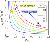
Fig. 11. Calculated threshold current density Jth for switching versus spin Hall angle θSH for various ratios of field-like effective field HFL to Slonczewski-like effective field HSL.
Download figure:
Standard image High-resolution image4.3. SOT switching in PtMn/[Co/Ni] system
In this section, we describe the SOT switching in a heterostructure with antiferromagnetic PtMn. Most of the studies on SOT switching have utilized nonmagnetic materials for the heavy-metal channel layer. Here, we show that antiferromagnetic PtMn also exhibit large enough SOT to induce magnetization switching. Moreover, owing to the exchange bias at the antiferromagnet/ferromagnet interface, this system allows field-free switching.
As described earlier, one can reverse perpendicular magnetization by SOT when breaking the rotational symmetry of the Slonczewski-like SOT by some means. The application of an in-plane field is a way of achieving this, but this is not appropriate for practical use in ICs. Previous studies demonstrated field-free switching in devices with lateral inversion asymmetry160) and tilted anisotropy,161) although they are not readily applicable for mass production. Antiferromagnetic materials are expected to provide a possible solution to this challenge. It is well known that they exhibit exchange bias at the interface with a neighboring ferromagnet.162) Moreover, a recent theoretical study showed that non-collinear antiferromagnets exhibit an intrinsic spin Hall effect163) and experimental works demonstrated inverse and direct spin Hall effects in some antiferromagnetic materials.164–167) Thus, we initially aimed to achieve field-free SOT switching in an antiferromagnet-ferromagnet bilayer system where the above two effects were utilized simultaneously.118)
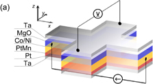
The film stack, device structure, and measurement setup are shown in Fig. 12(a). The deposited films were annealed at 300 °C for 2 h under an in-plane magnetic field of 1.2 T along the x-direction to provide the exchange bias. Magnetization curve measurement using a vibrating sample magnetometer revealed that the perpendicular easy axis and finite exchange bias can be obtained when the thickness of PtMn is in the range of 7.0–8.5 nm. The exchange bias field was obtained to be up to around 20 mT. Hall devices with a width of 10 mm were prepared through photolithography. For the measurement, a dc channel current ICH with a duration of 0.5 s was applied, which was followed by the detection of the Hall resistance RH originating from the anomalous Hall effect. All the measurements were performed at room temperature under zero magnetic field.
Download figure:
Standard image High-resolution image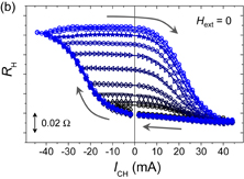
Fig. 12. (a) Stack structure, device structure, and measurement circuit. (b) Measured Hall resistance RH vs channel current ICH. The loop was measured while varying the magnitude of the maximum applied current.
Download figure:
Standard image High-resolution imageFigure 12(b) shows the obtained RH–ICH curves for a device with a PtMn thickness of 8.0 nm. The change in RH due to magnetization switching upon applying a current without an external field was obtained as expected. More interestingly, RH changes continuously with respect to the applied maximum ICH. Such analog-like behavior was not observed in previous Ta (or W)/CoFeB/MgO systems and is thus considered to be an inherent characteristic of the present material system. Note that, for devices with a PtMn thickness of less than 7.0 nm, which possess negligible exchange bias, generally observed square RH–ICH loops were obtained under the application of an in-plane field. Our following study elucidated that the analog feature is attributed to the variation of both the in-plane and perpendicular components of the exchange bias and that the magnetization reversal proceeds in a unit of the domain with a length scale of around 200 nm.168) We also note that field-free switching using antiferromagnetic materials was reported by different groups.119,169,170) Among them, Oh et al.119) utilized IrMn for the source of the in-plane field and SOT as in our work, whereas the others169,170) utilized Pt for the source of SOT and IrMn for the source of the in-plane field. Meanwhile, gradual magnetization reversal was observed by van den Brink et al.170) and Lau et al.169)
The analog-like switching observed in Fig. 12(b) is particularly interesting for applications to neuromorphic computing, or artificial intelligence, since this behavior is similar to that of synapses in the brain. In fact, devices that change their resistance continuously in response to the applied current are known as memristors,171,172) with which intensive studies have been performed to realize neuromorphic computing,173–175) where nanoscale Ag particles in a Si medium,173) a phase-change-based material,174) and the binary oxide Al2O3/TiO2−x175) were used. The suitability of spintronics devices for neuromorphic computing applications has also been pointed out recently.176,177) Using PtMn/[Co/Ni]-based SOT devices, we developed an artificial neural network as an example of neuromorphic computing operation and tested an associative memory operation.139) For the operation, the Hopfield model178) was used, which is known to be useful for emulating information processing in the brain.
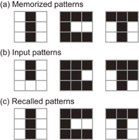
The prepared artificial neural network consists of a PC, a field-programmable gate array (FPGA), and 36 SOT devices. The experimental procedure is as follows. First, the system memorizes the three patterns, "I", "C", and "T", in 3 × 3 blocks shown in Fig. 13(a), from which the synaptic weight matrix in the Hopfield model is determined. Next, an input pattern, where one randomly selected element in the memorized pattern is inverted [examples are shown in Fig. 13(b)], is given. Then, the system executes an iterative learning process,179) where the analog nature of the SOT device as an artificial synapse is fully utilized. After the learning process, the system is expected to recall the memorized patterns as shown in Fig. 13(c). The degree of agreement between the memorized and recalled patterns was evaluated with the direction cosine, which becomes 1 for perfect matching. The ideal value of the direction cosine is 0.905 in the present test. We confirmed that the mean direction cosine was improved from 0.601 to 0.852 after the learning, demonstrating that our SOT devices can function as synapses with a learning function. A numerical simulation also revealed that it is effective to reduce the variation in the change in Hall resistance among the devices for a given channel current to realize reliable associative memory operation in large-scale systems.
Fig. 13. Patterns used for the associative memory operation experiment. (a) Memorized patterns. (b) Example of input patterns in which one block in the memorized patterns is flipped. (c) Recalled patterns restored by the artificial neural network through the learning process.
Download figure:
Standard image High-resolution image
5. Conclusions
This review article first explained the characteristics of three-terminal nonvolatile spintronics memories and the basic principle and key studies of current-induced DW motion and SOT-induced magnetization switching. Then, our recent studies on these techniques were reviewed. The three-terminal devices achieve high-speed and reliable operation due to the different current paths between the read and write operations, making them a promising replacement for high-speed volatile working memories such as SRAMs. Current-induced DW motion and SOT-induced magnetization switching can be applied to the write operation of nanoscale three-terminal devices. For the DW motion, a Co/Ni multilayer with a perpendicular easy axis was found to be a promising material system as it simultaneously provides a small threshold current density and high retention down to a device size of 20 nm. We found that the write current and time linearly decrease with decreasing device size and meet the requirement to replace SRAMs when the size is below around 50 nm, whereas a sufficiently large thermal stability factor can be maintained irrespective of the device size. A detailed analysis of the size dependence of the thermal stability factor provided a better understanding of its mechanism, in which a subvolume is excited, which governs the thermal stability, above a critical device size. We also showed that materials with higher magnetic anisotropy material are promising for achieving low-current DW motion in devices smaller than 20 nm. For SOT-induced switching, we showed that the discrepancy in the threshold current density between an experiment on micrometer-size devices with a Ta/CoFeB/MgO system and the macrospin-based theory can be partly explained by the spatial inhomogeneity and Joule heating, which become significant as the device scale increases. The remaining discrepancy observed in nanoscale devices can be mainly attributed to the field-like component of SOT, which was not considered in the previously developed theory. The threshold current density was found to strongly depend on the resistivity of the W channel and, for W/CoFeB/MgO, it was reduced to half of that for the Ta/CoFeB/MgO system when the W channel was sputtered at a low power and high pressure. We finally showed that the field-free switching of perpendicular magnetization is possible in an antiferromagnet-ferromagnet bilayer system due to the spin Hall effect of the antiferromagnet and the exchange bias at the interface. Moreover, the PtMn/[Co/Ni]-based device was found to show an analog-like switching, which also originates from the exchange bias. Employing this device as a synapse in an artificial neural network, we showed an associative memory operation as a proof-of-concept demonstration of neuromorphic computing.
As described here, three-terminal spintronics devices provide various opportunities ranging from high-speed nonvolatile memories used in leading-edge ICs to neuromorphic computing. With further advances, they will open a new era of electronics realizing safe, robust, and user-friendly electronic devices, information infrastructure, IoT societies, and artificial intelligence.
Acknowledgments
The authors wish to thank F. Matsukura, S. Ikeda, N. Kasai, H. Sato, M. Yamanouchi, Y. Horio, S. Sato, H. Akima, T. Endoh, T. Hanyu, M. Natsui, T. Dietl, M. Hayashi, T. Ono, D. Chiba, K.-J. Kim, Y. Nakatani, J. Ieda, T. Sugibayashi, N. Sakimura, N. Ishiwata, S. Miura, K. Kinoshita, H. Honjo, R. Nebashi, Y. Tsuji, M. Tada, T. Suzuki, T. Hirata, H. Iwanuma, Y. Kawato, K. Goto, C. Igarashi, N. Ohshima, I. Morita, S. DuttaGupta, C. Zhang, A. Kurenkov, K. Watanabe, T. Anekawa, T. Iwabuchi, and W. A. Borders for fruitful discussion and technical support. This work was supported in part by the FIRST Program of JSPS, the R&D Project for ICT Key Technology to Realize Future Society of MEXT, the ImPACT Program of CSTI, and JSPS KAKENHI Grant Numbers 15H05521 and 15K13964.