

Abstract
We report on the selective-area growth and characterization of wurtzite (WZ) InP/AlGaP core–multishell nanowires. Quantum well (QW) structures were fabricated in AlGaP multishells by changing the alloy composition. Transmission electron microscopy revealed that the AlGaP multishells were grown with a WZ structure on the side of the WZ InP core. The lattice constants of the WZ InP core and WZ AlGaP shell were determined by X-ray diffraction. Cathodoluminescence studies showed that the WZ AlGaP QW with an Al composition of 20% exhibited green emissions at 2.37 eV. These results open the possibility of fabricating green light-emitting diodes using WZ AlGaP-based materials.
Export citation and abstract BibTeX RIS
Color-mixed red–green–blue (RGB) light-emitting diodes (LEDs) are promising candidates for future solid-state lighting and display technology owing to their potential advantages in terms of energy conversion efficiency and color rendering index (CRI).1,2) However, achieving high-efficiency LEDs in the green region is challenging owing to a lack of suitable semiconductor materials; this region is known as the "green gap".3,4) Non-nitride III–V materials having wurtzite (WZ) structures have recently provided a new approach to overcoming this problem. Some theories predict that GaP and AlP in WZ structures have direct band gaps in contrast to conventional zinc blende (ZB) structures that have indirect band gaps.5–7) Although this new approach has been experimentally demonstrated in WZ GaP8,9) and WZ AlInP,10) such WZ materials with the quantum well (QW) structures required for LED applications have not been reported so far. In nanowire (NW) structures, radial core–multishell (CMS) NWs with QW structures are suitable for LED applications.11,12) In this study, we report the growth and characterization of WZ InP/AlGaP CMS NWs with QW structures for the green spectral region. The WZ AlGaP with an Al composition of approximately 20% is expected to have a band gap energy in the green spectral region on the basis of the calculations of their band structures.6,7)
CMS NWs were synthesized by selective-area metal organic vapor phase epitaxy (SA-MOVPE). In SA-MOVPE, InP NWs can be grown with a pure WZ structure by properly adjusting the growth conditions.13–15) The crystal structure transfer method16–18) was applied to these WZ InP NWs for radial multishell growth. First, a 20-nm-thick SiO2 layer was deposited on an InP (111)A substrate by plasma sputtering, and the SiO2 layer was partially removed by electron-beam (EB) lithography and wet chemical etching. SiO2 patterns were designed to be a periodic array of openings with a diameter of 130 nm. SA-MOVPE was performed in a low-pressure MOVPE reactor using trimethylaluminum (TMAl), trimethylgallium (TMGa), trimethylindium (TMIn), and tertiarybutylphosphine (TBP) as source materials. Prior to the growth, the native oxide on the openings was removed by thermal cleaning for 5 min at 600 °C in hydrogen and TBP ambient. After thermal cleaning, WZ InP NWs were grown for 15 min at 660 °C with a V/III ratio of 18, which is the typical condition for growing WZ structures.13) The partial pressures of TMIn and TBP were 2.7 × 10⁻⁶ and 4.9 × 10⁻⁵ atm, respectively. Low-temperature (LT) AlGaP shells were then grown for 7 min at 600 °C with a V/III ratio of 650 to prevent P desorption from InP NWs. The respective partial pressures of TMAl, TMGa, and TBP were 2.4 × 10⁻⁷, 2.4 × 10⁻⁷, and 3.1 × 10⁻⁴ atm, which correspond to the TMAl supply ratio, [TMAl]/([TMAl] + [TMGa]), of 0.50 in the vapor phase. After LT AlGaP shell growth, three AlGaP shell layers were grown to fabricate QW structures by changing the TMAl supply ratios. The inner barrier layer was grown for 20 min at 750 °C with a V/III ratio of 320. The respective partial pressures of TMAl, TMGa, and TBP were 4.8 × 10⁻⁷, 4.8 × 10⁻⁷, and 3.1 × 10⁻⁴ atm, which correspond to the TMAl supply ratio of 0.50 in the vapor phase. The QW layer was grown for 3 min at 700 °C with a V/III ratio of 320. The respective partial pressures of TMAl, TMGa, and TBP were 1.9 × 10⁻⁷, 7.7 × 10⁻⁷, and 3.1 × 10⁻⁴ atm, which correspond to the TMAl supply ratio of 0.20 in the vapor phase. The outer barrier layer was grown for 10 min at 700 °C with a V/III ratio of 320. The partial pressures of TMAl, TMIn, and TBP were the same as those of the inner barrier layer. Finally, the GaP shell was grown for 1 min at 700 °C with a V/III ratio of 650 as a capping layer to prevent oxidation of AlGaP. The partial pressures of TMGa and TBP were 9.6 × 10⁻⁷ and 6.2 × 10⁻⁴ atm, respectively.
The morphology, crystal structures, and compositions of CMS NWs were characterized by scanning electron microscopy (SEM), transmission electron microscopy (TEM), and energy dispersive X-ray spectroscopy (EDX) combined with scanning transmission electron microscopy (STEM). The electron-beam projection was parallel to the  direction. X-ray diffraction (XRD) measurements were carried out to investigate the crystal structures of the NW assembly. The NW pitch was 1600 nm and the investigated sample area was about 4 mm2, in which more than one million NWs were included. Cathodoluminescence (CL) measurements were performed at 34 K on a single CMS NW with an acceleration voltage of 7 kV. On the basis of the calculation by Kanaya and Okayama,19) the penetration depth of electrons was about 500 nm under this condition, whereas most of the electrons were generated within a fraction of the penetration depth.
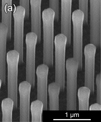
An SEM image and a schematic illustration of InP/AlGaP CMS NWs with QW structures are shown in Figs. 1(a) and 1(b). The NWs resembled hexagonal pillars with  side facets. The NW pitch was 600 nm. The average height and total diameter of the CMS NWs were 2.6 µm and 240 nm, respectively. A slightly larger diameter was found at the tip of the NWs, which corresponds to the AlGaP shell grown on top of the InP core. From the SEM image, no tapering or bending of the NWs were observed, while polycrystal deposition on SiO2 films was observed. The deposition began to appear when the AlGaP shell growth time was 20 min or more.
Download figure:
Standard image High-resolution image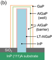
Fig. 1. (a) 30°-tilted-view SEM image of InP/AlGaP CMS NWs. (b) Schematic illustration of grown layers of the CMS NW.
Download figure:
Standard image High-resolution imageTo confirm QW structures fabricated in the AlGaP shell, we investigated the compositions of the CMS NWs by EDX measurements. A high-angle annular dark-field (HAADF) STEM image of a NW cross section of the middle part and corresponding EDX mappings are shown in Figs. 2(a)–2(e). From these images, the diameter of the InP core and the thickness of the AlGaP shell were determined to be approximately 125 and 50 nm, respectively. The QW thickness was about 3 nm. The two barrier layers had different thicknesses because the growth time of the outer barrier layer was shorter than that of the inner barrier layer. This is also because the growth rate of the outer AlGaP shell decreased as the growth time increased probably owing to the increasing amount of polycrystals deposited on the SiO2 mask area.

Download figure:
Standard image High-resolution image
Download figure:
Standard image High-resolution image
Fig. 2. (a) Cross-sectional HAADF STEM image of a CMS NW and corresponding EDX mappings of (b) In, (c) P, (d) Al, and (e) Ga, showing the existence of a QW structure. (f) EDX line scan of a CMS NW along the lateral direction and corresponding HAADF STEM image (inset).
Download figure:
Standard image High-resolution imageFigure 2(a) shows two types of black contrast. The black contrast around the InP core resulted from the low crystal quality of the LT AlGaP shell layer. The other black contrast along the  radial directions was due to aluminum segregation, which commonly appears in aluminum-containing shell layers, such as GaAs/AlInP core–shell NWs.20) Aluminum segregation was also found in EDX mappings in Figs. 2(d) and 2(e). In addition to aluminum segregation, indium diffusion appeared in the AlGaP shell, which can be seen in both the EDX mapping and the line scan in Figs. 2(b) and 2(f), respectively. The reason for this indium diffusion is that the growth temperature of the AlGaP shell is higher than that of the InP core. From Fig. 2(f), the aluminum and gallium compositions in the barrier layers were almost the same, excluding the effect of indium diffusion, which is equal to the supply ratio of TMAl and TMGa. Therefore, the aluminum and gallium compositions in the QW layer were estimated to be 20 and 80%, respectively.
To confirm the crystal structures of a CMS NW, we performed TEM and fast-Fourier-transform (FFT) analyses of a NW, and the results are shown in Fig. 3. Three parts of the NW were investigated. First, the InP core had a WZ structure with a few stacking faults per micrometer. Second, the AlGaP shell on top of the InP core had a ZB structure with stacking faults. In Fig. 3(a), the diameter of the top part of the NW was larger than that of the middle part. This is another piece of evidence showing that the AlGaP shell on the top consists of ZB structures because stacking faults and lateral growth continuously occur until stable  facets are formed in the case of selective-area growth of NWs with ZB structures.14,21) Third, the AlGaP shell on the side of the InP core mainly had a WZ structure, but it partly had a ZB structure resulting from stacking faults. The appearance ratio of WZ segments in the AlGaP shell was calculated to be 84% by statistical analysis.22) We consider that the stacking faults and ZB segments appeared at the interface of the InP core and AlGaP shell for the following reasons. For planar layers, the critical thickness is calculated to be less than 1 nm from the lattice mismatch of 7.0% between InP and Al0.5Ga0.5P. When the AlGaP shell is grown on the InP core, it can be coherently grown on the InP core until it reaches a critical thickness, and then misfit dislocations appear in the AlGaP shell. As a result, additional layers are introduced in WZ layers of the AlGaP shell that has a smaller lattice constant, resulting in ZB segments such as "ABABCBCB⋯" and "ABACABAB⋯".
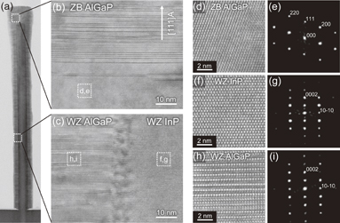
Fig. 3. Cross-sectional TEM images of an InP/AlGaP CMS NW. The incidence of the electron beam was parallel to the  direction of the substrate. (a) Overall TEM image of the NW. (b) and (c) Enlarged TEM images of the top and side of the NW shown in (a). (d)–(i) High-resolution TEM images and corresponding FFT images of the top AlGaP shell, side AlGaP shell, and InP core.
Download figure:
Standard image High-resolution imageFigure 4 shows an XRD reciprocal space mapping (RSM) around the ZB (331) reflection of the InP (111)A substrate. The WZ  and ZB (331) peaks were observed for the InP core and substrate, and the WZ
  , ZB (224) twin, and faint ZB (331) peaks were observed for the AlGaP shell. The strong intensity of the WZ InP
  peak indicates that the InP core has a high crystal quality in the WZ structure. In contrast, the intensity of the WZ AlGaP
  peak was relatively low and broad owing to the low crystal quality resulting from stacking faults. The ZB (224) twin peak and faint spot of ZB (331) for AlGaP were attributed to the ZB AlGaP shell with rotational twins grown on the top of the InP core, because no ZB (224) twin peak was observed for both the InP core and substrate. These results are in good agreement with those of TEM analysis.
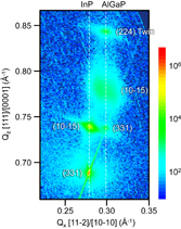
Fig. 4. XRD RSM of InP/AlGaP CMS NWs recorded around the ZB (331) reflection of the InP (111)A substrate.
Download figure:
Standard image High-resolution imageNext, we measured the axial and radial lattice constants, cWZ and aWZ, of the WZ InP core and WZ AlGaP shell from the peak positions of WZ  reflections, and compared the measured values with relaxed WZ lattice constants geometrically converted from ZB lattice constants. For the conversion, the relations
  and
and  were used, and Vegard's law was applied to the calculations of AlGaP lattice constants. The calculation results are summarized in Table I. For WZ InP, both the measured aWZ and cWZ values were almost the same as the converted aWZ and cWZ values. Kriegner et al. have reported that free-standing WZ InP is elongated in the c-axis direction and compressed in the a-axis direction as compared with the converted values.23) These tendencies were also found in other III–V NWs.24,25) However, in this study, no such tendency was found probably because the WZ InP core was surrounded by an AlGaP shell that has a smaller lattice constant and was therefore subject to compressive strain in the c-axis direction. For WZ AlGaP, both the measured aWZ and cWZ values were substantially larger than the converted aWZ and cWZ values. This implies the incorporation of InP, which has a larger lattice constant. The measured lattice constants of WZ AlGaP correspond to those of WZ AlGaInP with about 10% indium when they are geometrically converted using Vegard's law. This result is consistent with the EDX analysis results shown in Fig. 2.
Table I. WZ lattice constants of the InP core and AlGaP shell.
| Material | Method | a (Å) | c (Å) | c/a |
|---|---|---|---|---|
| WZ InP | Conversion | 4.1498 | 6.7766 | 1.633 |
| Experimentala) | 4.1423 | 6.8013 | 1.642 | |
| This work | 4.15 | 6.77 | 1.63 | |
| WZ Al0.5Ga0.5P | Conversion | 3.8587 | 6.3012 | 1.633 |
| This work | 3.93 | 6.43 | 1.64 |
a) From Ref. 23.
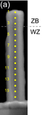
To understand the effects of WZ and ZB structures on optical properties, we carried out CL measurements of a single NW at 34 K. The electron beam was scanned along the NW axis with 16 measured points at intervals of about 150 nm, as shown in Fig. 5(a). The obtained CL spectra are shown in Fig. 5(b). For clarity of CL peak energies, representative CL spectra of the top and middle of the NW are shown in Fig. 5(c) in a logarithmic scale. The peaks at 1.42 and 1.62 eV correspond to emissions from the ZB InP substrate and WZ InP core NW. The peaks at 1.36–1.38 eV, observed at beam positions #15 and #16 in Fig. 5(b), correspond to bound exciton and donor–acceptor emissions of the InP substrate.26) The peak energy for ZB InP is equivalent to the known value, whereas the peak energy for WZ InP is slightly higher than those previously reported.13) The theoretical band gap energy of WZ InP is 1.502 eV, and the band gap energy of previously reported WZ InP NWs is 1.54 eV. In this study, the WZ InP core has compressive strain arising from the AlGaP shell, which can lead to an increase in band gap energy. If the band gap energy of the WZ InP NWs is the same as that previously reported, the effect of compressive strain will lead to an energy shift of 80 meV.
Download figure:
Standard image High-resolution image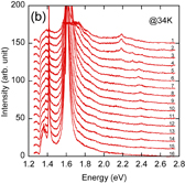
Download figure:
Standard image High-resolution image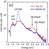
Fig. 5. CL spectra of a single InP/AlGaP CMS NW measured at 34 K. The electron beam was scanned along the NW axis. (a) Measured points and (b) corresponding CL spectra of the NW. (c) Representative CL spectra of the top and middle of the NW shown in a logarithmic scale.
Download figure:
Standard image High-resolution image
Regarding the AlGaP multishell, CL emissions were observed at 2.18 and 2.37 eV. From the electron beam spot, the former can be attributed to ZB AlGaP at the top of the InP core, and the latter can be attributed to WZ AlGaP on the side. We consider that these two emissions originated from the AlGaP QWs because we found in a similar material combination that simple core–shell NWs without QW structures exhibited no CL emissions from the shells. Although the origin of the peak at 2.30 eV observed at beam positions #3–#5 in Fig. 5(b) was unclear, it was probably related to WZ/ZB type II junctions at the interface of WZ and ZB AlGaP shells. The reason for the low emission intensity was that the generated electron–hole pairs were easily moved from the AlGaP shell to the InP core. The results indicate that green emissions at 2.37 eV (523 nm) were evident from the WZ AlGaP QW, which had a shorter wavelength than reported ones.8,10)
The band gap of WZ Al0.2Ga0.8P is estimated to be 2.394 eV by linear approximation from the values found in the literature.6,27) WZ Al0.5Ga0.5P/Al0.2Ga0.8P/Al0.5Ga0.5P QW is predicted to show type I band alignment with the conduction and valence band offsets of 93 and 112 meV, and the quantum-confinement effect of 3-nm-thick QW leads to an energy blue shift of 111 meV. In addition, the effect of incorporating 10% indium, which was suggested from XRD and EDX measurements, leads to an energy red shift of 92 meV. Therefore, the emission energy of our WZ QW is estimated to be 2.413 eV. This estimation is consistent with the experimental result. Calculation based on a ZB QW gave similar confinement energy and red shift owing to indium incorporation; thus, this ZB QW is less likely. However, the analysis of the nature of these emissions in greater detail is difficult at present and strain effects and the variations in the composition and the QW thickness should be considered to achieve more accurate assessment. In this regard, other optical investigations, such as time-resolved measurements, are required to clarify whether WZ AlGaP QWs have direct band gaps.
In summary, we investigated the growth morphology, composition, and structural and optical properties of WZ InP/AlGaP CMS NWs grown by the crystal structure transfer method. Cross-sectional STEM and EDX images showed that the QW structures were formed in the AlGaP multishell. TEM analysis revealed that the InP core had a WZ structure with very few stacking faults and that the AlGaP multishell was grown with a WZ structure on the side of the InP core, whereas it was grown with a ZB structure at the top. From XRD measurements, the measured lattice constants of WZ InP were found to be almost the same as the calculated values, while those of WZ AlGaP were larger owing to indium outdiffusion. Finally, we observed green emissions at 2.37 eV from the WZ AlGaP QW and showed that a difference in crystal structure affects the CL emission energy in AlGaP QWs. Our results demonstrate a pathway for preparing green LEDs using WZ AlGaP-based materials.
Acknowledgements
The authors would like to thank Professor Shinjiro Hara and Dr. Keitaro Ikejiri for their valuable advice, as well as Dr. Masatoshi Yoshimura, Dr. Eiji Nakai, and Mr. Muyi Chen for their support in the experiments. This work was financially supported by a Grant-in-Aid for Scientific Research (S) (KAKENHI Grant Number 23221007) provided by the Japan Society for the Promotion of Science (JSPS).