

Abstract
We present the world's first charge-recycling-based low-power technique of complementary metal–oxide–semiconductor (CMOS) magnetic cell manipulation. CMOS magnetic cell manipulation associated with magnetic beads is a promissing tool for on-chip biomedical-analysis applications such as drug screening because CMOS can integrate control electronics and electro-chemical sensors. However, the conventional CMOS cell manipulation requires considerable power consumption. In this work, by concatenating multiple unit circuits and recycling electric charge among them, power consumption is reduced by a factor of the number of the concatenated unit circuits (1/N). For verifying the effectiveness, test chip was fabricated in a 0.6-µm CMOS. The chip successfully manipulates magnetic microbeads with achieving 49% power reduction (from 51 to 26.2 mW). Even considering the additional serial resistance of the concatenated inductors, nearly theoretical power reduction effect can be confirmed.
Export citation and abstract BibTeX RIS
1. Introduction
On-chip biomedical analysis using complementary metal–oxide–semiconductor (CMOS) electronics is key technology for point-of-care-testing (POCT) technology. Since CMOS can integrate control electronics and electrochemical sensor,1–12) the form factor for biomedical analysis can be dramatically reduced. Additionally, CMOS electronics reduces its fabrication cost and has high scalability.13–16)
For integrating cell manipulation as well as electrochemical sensors into CMOS electronics, CMOS magnetic cell manipulation platform for drug screening was developed.17–19) By applying current into on-chip micro coil and generating magnetic field, the biological cells with magnetic beads can be manipulated. On-chip micro coil was realized by interconnection of CMOS fabrication. The conventional CMOS magnetic cell manipulation platform successfully demonstrated its effectiveness. However, power consumption of the conventional CMOS cell manipulation is quite high (50 mW per one cell manipulation unit). This large power consumption increase temperature, which degrades the stability. Thus, low-power technique must be developed for practical application.
For satisfying the requirement, in this work, we propose power reduction technique in CMOS magnetic cell manipulation platform by using charge recycling technique for the first time. By concatenating multiple unit circuits and recycling electric charge among them, power consumption can be reduced by a factor of the number of the concatenated unit circuits (1/N, where N is the number of the concatenated units). In order to verify the effectiveness of the proposed approach, a test chip was fabricated in a cost-competitive 0.6-µm CMOS technology. The measurement results successfully demonstrated 49% power reduction by concatenating two cell manipulation units, which agree well with the theoretical expectation.
The paper is organized as follows: Sect. 2 presents the proposed low-power CMOS magnetic cell manipulation platform. Section 3 introduces design of the test chip for verify the effectiveness of the proposed approach. The measurement results are shown in Sect. 4. Section 5 concludes this paper.
2. Low-power CMOS magnetic cell manipulation using charge recycling technique
2.1. Operation principle of magnetic manipulation
Figure 1 shows the operation principle of magnetic manipulation. By applying current into on-chip micro coil and generating magnetic field, drawing [Fig. 1(a)] and detaching [Fig. 1(b)] magnetic microbeads can be feasible. By combining drawing and detaching function in adjacent manipulation units, magnetic manipulation can be achieved. Since magnetic manipulation requires drawing and detaching function, the magnetic manipulation cell must have flexibility in current direction.
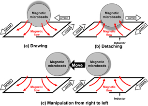
Fig. 1. Operation principle of the CMOS cell manipulation platform.
Download figure:
Standard image High-resolution image2.2. Motivation for power reduction
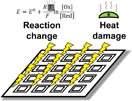
Figure 2 shows the motivation of the proposed low-power CMOS magnetic cell manipulation platform. The conventional magnetic cell manipulation17) exploits a low-duty driving pulse current for low-power operation. However, it requires large power consumption. The measured power consumption is 50 mW per one cell manipulation unit, which corresponds to total power consumption of 3.2 W when considering 8 × 8 array arrangement.
Download figure:
Standard image High-resolution image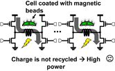
Fig. 2. Motivation of developing the proposed low-power CMOS cell manipulation platform.
Download figure:
Standard image High-resolution imageThis large power consumption increases the temperature that damages the manipulated biological objects, changes the chemical reactions' activity (for example, the Nernst equation contains temperature), and makes it difficult to apply POCT applications. In order to achieve magnetic cell manipulation with maintaining biological and chemical environment and enabling POCT application, power reduction technique must be developed.
2.3. Principle of power reduction by using the proposed platform
Figure 3 shows the conceptual diagram of the proposed low-power CMOS magnetic cell manipulation platform using charge recycling technique. Charge recycling technique is commonly used for low-power operation in solid-state circuit design.20–23) By using electronic charge multiple times, power can be reduced. The charge recycling technique was intensely developed for power reduction of logic circuits.
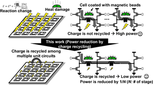
Fig. 3. Concept of the proposed low-power CMOS cell manipulation platform using charge recycling technique.
Download figure:
Standard image High-resolution imageIn our research, by concatenating adjacent manipulation cell circuits and recycling electric charge (current) among them, power consumption per one unit can be reduced by a factor of the number of concatenated circuits (1/N, where N is the number of the concatenated units). For instance, by concatenating two manipulation cell circuits, 50% power reduction can be achieved. The concept has been established in the transmitter design in the inductive-coupling proximity wireless communication.24–28) Previous reports has achieved power reduction which agrees well with the theoretical value. One of the reports25) achieved approximately 70% power reduction by concatenating four inductors, which is almost identical to the theoretical value (1/4, 75% power reduction).
Figure 4 shows the circuit diagram and operation image of the proposed low-power CMOS cell manipulation platform using charge recycling technique. In Fig. 4, it is assumed that the current flown from right to left generates magnetic flux enabling drawing function and the current of its reverse direction generates that enabling detaching function. The H-bridge charge recycling circuit architecture was adopted. In the upper part of Fig. 4, the PMOS on the left end and the NMOS on the right end are both on. The current flows from left to right and generates magnetic flux enabling drawing function. While, in the lower part of Fig. 4, the PMOS on the right end and the NMOS on the left end are both on. The current flows from right to left and generates magnetic flux enabling detaching function.
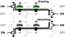
Fig. 4. Circuit diagram and operation image of the proposed low-power CMOS cell manipulation platform using charge recycling technique.
Download figure:
Standard image High-resolution imageThere are two advantage of adopting the H-bridge charge recycling circuit architecture. One is that the effectiveness of this architecture has been verified in the previous reports.24–28) The other is that this architecture allows flexibility in current direction (manipulation's direction, drawing or detaching).
3. Test chip design and measurement setup
3.1. Test chip design
For verifying the effectiveness, test chip was fabricated in a cost-competitive 2-poly 3-metal 0.6-µm standard CMOS technology. The supply voltage is 5 V. Figure 5 shows the test chip microphotograph. The test chip contains the proposed magnetic manipulation and I/O circuits. Since the number of stages of implemented magnetic manipulation is two, approximately 50% power reduction is expected. I/O circuits were implemented for delivering signal from/to the core circuits to/from I/O pad.
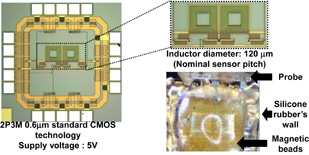
Fig. 5. Test chip microphotograph.
Download figure:
Standard image High-resolution imageThe diameter of implemented on-chip inductor (micro coil) is 120 µm. The diameter is determined to be identical with the pitch of the potentiometric sensor.29–31) The on-chip inductor was formed by aluminium on-chip interconnect which is available in standard CMOS process. Thus, no post-CMOS process was needed, which reduces fabrication cost. In design of the on-chip inductor, there is a trade-off between self inductance and parasitic resistance. For instance, large number of turns and narrow interconnect width allows large self inductance but causes large parasitic resistance. Design parameter of the inductor such as line width and the number of turns was determined while considering this trade-off.
In this study, we have implemented 30-turn inductor. The inductor is formed by thin 2nd metal layer and thick 3rd metal layer. In order to minimize the gap of resistance between 2nd-layer and 3rd layer parts, wide and narrow interconnect is used in 2nd and 3rd layer, respectively. As a result, the number of turns are 19 in 3rd layer and 11 in 2nd layer. Based on the previous report,32) we have calculated the electrical property of the implemented inductor. The calculated value of total inductance and parasitic resistance are 230 nH and 50 Ω, respectively.
The driver transistors consists of three NMOSs and three PMOSs. The middle NMOS and PMOS are twice larger than the edge NMOSs and PMOSs. The occupied area of the driver transistors is 120 × 60 µm2, which can be implemented under the on-chip inductor.
3.2. Measurement setup
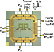
The test chip was measured by manual probing using a manual probe station (Apollowave MP-150). In order to prevent micro probes from electrical short by solution, we have developed silicone rubber's wall by hand. To form silicone rubber's wall, silicone paste (Momentive Performance Materials TSE3826) was used. The supply voltage was supplied by the power source (Keysight Technologies E3621) and the control signal was supplied by the multifunction waveform generator (NF WF1974).
To demonstrate the feasibility of magnetic cell manipulation, we have performed manipulation of magnetic microbeads using the test chip. The magnetic microbeads (Dynal Biotech M-280, 2.8-µm diameter, magnetic susceptibility is 0.17) was used for the measurement. The magnetic microbeads floated in the solution (PBS, pH 7.4 with 0.01% Tween®-20 and 0.02% NaN3 added as preservatives). The magnetic microbeads were dropped to the silicone rubber's wall on the fabricated test chip using micro pipet.
3.3. Measurement condition
Figure 6 shows the measurement condition for demonstrating the manipulation of the magnetic microbeads using the proposed technique. In order to demonstrate the drawing function, we have set the signal condition that is identical to the upper part of Fig. 4. When the control pulse is high, the PMOS on the left end and the NMOS on the right end are both on. The current flows from left to right and generates magnetic flux enabling drawing function while achieving 50% power reduction.
Download figure:
Standard image High-resolution image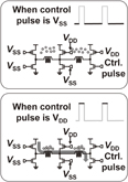
Fig. 6. Measurement condition of manipulation of magnetic microbeads.
Download figure:
Standard image High-resolution image4. Measurement results
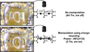
Figure 7 shows the measured results of manipulation of the magnetic microbeads. We confirmed that only when supplying control signal, microbeads were manipulated as designed. The chip successfully manipulates microbeads with achieving 49% energy reduction (the required power was reduced from 51 to 26.2 mW), which agree well with the theoretical expectation (50%). Even considering increase of serial resistance, nearly theoretical energy reduction effect can be obtained. This measurement results validates the effectiveness of the proposed technique.
Fig. 7. Measured results of manipulation of magnetic microbeads.
Download figure:
Standard image High-resolution image
5. Conclusions
In this paper, we proposed a low-power CMOS magnetic cell manipulation platform using charge recycling technique for the first time. By concatenating multiple unit circuits and recycling electric charge among them, power consumption can be reduced by a factor of the number of the concatenated unit circuits (1/N). For verifying the effectiveness, test chip was fabricated in 0.6-µm CMOS. By measuring the test chip, nearly theoretical power reduction effect (49%) was successfully confirmed.
Acknowledgments
The fabrication of CMOS chips was supported by Taiwan Semiconductor Manufacturing Co., Ltd. (TSMC, Taiwan), and the VLSI Design and Education Center (VDEC), University of Tokyo in collaboration with Synopsys, Inc. and Cadence Design Systems, Inc. This research was financially supported by Grants-in-Aid for Scientific Research (S) (Nos. 20226009 and 25220906) from the Ministry of Education, Culture, Sports, Science and Technology of Japan, by JST, PRESTO, by the Strategic Information and Communications R&D Promotion Programme (Nos. 121806006, 152106004) of the Ministry of Internal Affairs and Communications, Japan, by TOYOTA RIKEN, and by The Nitto Foundation.