
Abstract
To suppress the reverse recovery surge voltage of silicon power diodes, the effects of adjusting trap energy levels through local lifetime control were investigated by device simulation and theoretical analysis of the Shockley–Read–Hall (SRH) model. In general, local lifetime control techniques localize carrier traps at the anode side of a diode and optimize the carrier lifetime profile to suppress surge voltage. However, the suppression effect of a certain localized trap density distribution on surge voltage varies with a change in trap energy level, even if the trap density distribution is the same. It became clear that deep trap energy levels suppress surge voltage more than shallow trap energy levels at 1000 A/cm2 or less. Thus, deep trap energy levels such as Et − Ei = 0.0–0.2 eV are favorable for suppressing surge voltage in almost all power devices.
Export citation and abstract BibTeX RIS
1. Introduction
Silicon power diodes are widely used in applications such as home electric appliances and hybrid vehicles, and it is increasingly demanded that their reliability be improved. Reverse recovery surge voltage is one important reliability issue, because surge voltage causes avalanche breakdown and electromagnetic interference noise.1–4) Hence, methods of suppressing the reverse recovery surge voltage of silicon power diodes are being investigated.
During the on-state of a diode, minority excess carriers are injected into the drift region from the anode and cathode layers. In the transition from the on-state to the off-state, excess carriers are removed from the drift layer, producing a reverse recovery current.1,5,6) A high current change rate (di/dt) and a large parasitic inductance cause high surge voltage.1) The di/dt value is determined by an excess carrier distribution in the drift region immediately before a reverse recovery.1,6) Nowadays, there are two techniques commonly used for obtaining an optimum excess carrier distribution. One is carrier injection control and the other is local lifetime control. For example, an emitter-controlled (EMCON) diode,7,8) the diode with controlled injection of back-side holes (CIBH),9,10) the merged PiN/Schottky (MPS) diode,11,12) and other diodes13–15) are used in carrier injection control. On the other hand, noble metal atom diffusion and charged particle irradiation are used in local lifetime control.16–21)
In previous studies, local lifetimes were controlled by localizing carrier traps. In other words, the carrier lifetime profile is generally controlled by adjusting the trap distribution.16–20) However, in fact, reverse recovery characteristics are also affected by trap energy levels.22–24) We previously verified that variations in recombination rate due to the difference in trap energy level affect surge voltage.25) However, in our previous study, we investigated only a flat trap density distribution and did not consider local lifetime control.
Therefore, in this study, we clarify the effect of local lifetime control on the suppression of surge voltage through the adjustment of trap energy level, and develop guidelines for suppressing surge voltage through the design of silicon power diodes.
2. Methods
To determine the trap energy level that effectively suppresses surge voltage, we have to clarify the relationship among the surge voltage, the carrier lifetime, and the trap energy level.
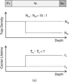
First, the relationship between the carrier lifetime profile and the surge voltage was calculated by device simulation using the Sentaurus Device (Synopsys). We simulated the P+ N− N+ diode structure and carrier lifetime profiles shown in Fig. 1. τa and τc are the carrier lifetimes of the anode and cathode sides, respectively. It is assumed that τc is larger than τa, and that the carrier lifetime ratio is defined as τc/τa.
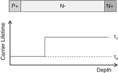
Fig. 1. Schematic model used for simulation.
Download figure:
Standard image High-resolution imageSecond, the relationship between the carrier lifetime and the trap energy level was analyzed by theoretical analyses with the Shockley–Read–Hall (SRH) model.26,27) Table I shows a lists of the definition of symbols and parameters used for the calculation. Assuming a single trap energy level, the total recombination rate Rr in the N-drift region is expressed as

where Rbulk and Rtrap are the recombination rate in the bulk silicon substrate and the recombination rate due to the trap, respectively. Under high injection conditions ( ), Rbulk and Rtrap can be approximated as28,29)
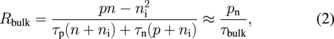
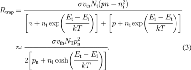
Table I. Definitions of symbols and parameters used for calculation.
| Symbol | Definition | Symbol | Definition |
|---|---|---|---|
| Rr | Total recombination rate | Nt | Trap density |
| Rbulk | Intrinsic recombination rate | τ | Total carrier lifetime |
| Rtrap | Trap recombination rate | τp | Intrinsic hole lifetime |
| p | Hole density | τn | Intrinsic electron lifetime |
| n | Electron density | τbulk | Intrinsic carrier lifetime |
| pn | Excess carrier density | Et | Trap energy level |
| ni | Intrinsic carrier density | Ei | Mid band energy level |
| σ | Capture cross section | k | Boltzman constant |
 |
Thermal velocity | T | Temperature |
From Eqs. (1)–(3), the following relationship among the excess carrier density pn, the recombination rate Rr with various trap energy levels, and the total carrier lifetime τ in the drift region is established as
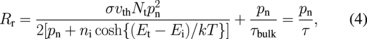
where σ is the capture cross section,  is the thermal velocity, Nt is the trap density, and τbulk is the intrinsic carrier lifetime in the bulk silicon substrate.
Finally, from these calculations, we investigate the trap energy levels that are effective for the suppression of the surge voltage.
3. Results and discussion
3.1. Device simulation analysis: carrier lifetime profile dependence of reverse recovery surge voltage
Figure 2 shows simulated forward current voltage curves of diodes with various carrier lifetime ratios τc/τa at a temperature of 300 K. Traps were not defined in this simulation. The average carrier lifetime was adjusted to match the forward voltage drop at 200 A/cm2 for each lifetime ratio. Figure 3 shows the dependence of the hole density distribution on τc/τa. The position of the minimum carrier density is found at the center of the drift region when the carrier lifetime profile of the diode is flat (τc/τa = 1). This position moves toward the anode with an increase in τc/τa.
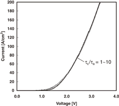
Fig. 2. Simulated current–voltage curves for various carrier lifetime ratios (T = 300 K).
Download figure:
Standard image High-resolution image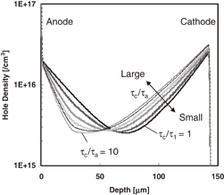
Fig. 3. Simulated hole density distributions for various carrier lifetime ratios (T = 300 K).
Download figure:
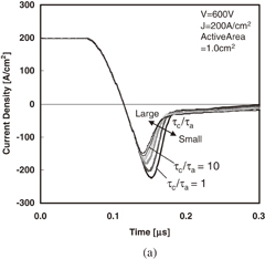
Standard image High-resolution imageFigures 4(a) and 4(b) show the calculated dependences of reverse recovery current and voltage waveforms, respectively, on τc/τa with an inductive load in a double-pulse mode. The reverse recovery waveform exhibited a soft recovery with an increase in τc/τa. Figure 5 shows the relationship between the surge voltage and the τc/τa obtained from Fig. 4. The flat carrier lifetime profile (τc/τa = 1) diode exhibited the highest surge voltage. The anode side lifetime τa decreased and the cathode side lifetime τc increased, resulting in a low surge voltage. Therefore, the surge voltage can be suppressed by increasing τc/τa.
Download figure:
Standard image High-resolution image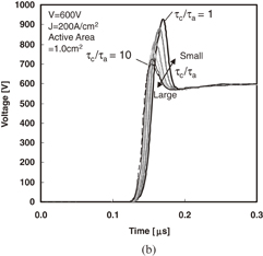
Fig. 4. Simulated reverse recovery (a) current and (b) voltage waveforms for various carrier lifetime ratios (T = 300 K).
Download figure:
Standard image High-resolution image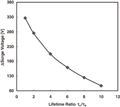
Fig. 5. Simulated carrier lifetime ratio dependence of surge voltage (T = 300 K).
Download figure:
Standard image High-resolution image3.2. Theoretical analysis: trap energy level dependence of carrier lifetime profile
Figure 6(a) shows the schematic structure of a P+ N− N+ diode that we used for theoretical and numerical analysis models. The anode side trap density Nta is ten times higher than the cathode side trap density Ntc in all analyses. To investigate the effects of various trap energy levels, Nta/Ntc was maintained constant. Figure 6(b) shows a band diagram of a trap. We define the trap energy levels near the midpoint of the band gap as deep levels and those near the conduction or valence band as shallow levels.
Download figure:
Standard image High-resolution image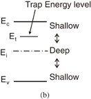
Fig. 6. Schematic (a) diode model and (b) band diagram used for theoretical and numerical analyses.
Download figure:
Standard image High-resolution imageFigure 7 shows the correlation between the recombination rate and the excess carrier density, calculated with Eq. (4), in the cases of Et − Ei = 0.1 eV (example of deep level) and Et − Ei = 0.4 eV (example of shallow level). The trap density was adjusted to match the recombination rate at pn = 4 × 1016 cm−3 for each trap energy level. It can be assumed that the diodes of the two trap energy levels have the same forward voltage drop at about 200 A/cm2. Note that the slope of the Et − Ei = 0.1 eV line is constant, whereas that of the Et − Ei = 0.4 eV line varies with carrier and trap densities. This difference is due to a difference in the probability of carrier emission from a trap. The probability of carrier emission is proportional to the term ni cosh{(Et − Ei)/kT} in Eq. (4). This term increases exponentially with an increase in [Et − Ei]. At deep levels, Et − Ei is small, and the value of that term is negligible. In this case, Eq. (4) can be approximated as
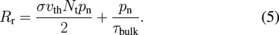
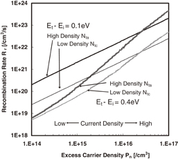
Fig. 7. Calculated correlation between recombination rate and excess carrier density (T = 300 K).
Download figure:
Standard image High-resolution imageEquation (5) indicates that the recombination rate is proportional to the excess carrier and trap densities. On the other hand, at shallow levels, the effect of that emission probability term cannot be ignored. This difference in slope makes the carrier lifetime dependent on multiple factors.
Because carrier lifetime is inversely proportional to recombination rate, it can be calculated as follows from Eq. (4):
Figure 8 shows the correlation between the carrier lifetime and the excess carrier density, calculated from Eq. (6). In the case of Et − Ei = 0.1 eV, the carrier lifetime is constant. In contrast, in the case of Et − Ei = 0.4 eV, the carrier lifetime varies with the excess carrier and trap densities. This means that the delta of carrier lifetime between high and low trap densities in the case of Et − Ei = 0.1 eV is constant, unaffected by the excess carrier density, and that this delta in the case of Et − Ei = 0.4 eV changes with the excess carrier density.
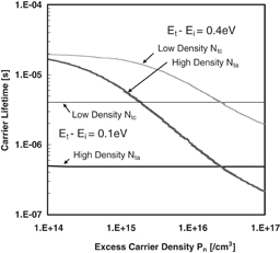
Fig. 8. Calculated correlation between carrier lifetime and excess carrier density (T = 300 K).
Download figure:
Standard image High-resolution imageThe carrier lifetime ratio τc/τa can be established from Eq. (6) as

At the deep level, Eq. (7) can be approximated as
Equation (8) indicates that τc/τa is independent of the excess carrier density at the deep level. Figure 9 shows the relationship between τc/τa and the trap energy level, calculated from Eq. (7). With deep levels such as Et − Ei = 0.0–0.2 eV, the same τc/τa is maintained at any excess carrier density. This is explained by Eq. (8). With shallow levels such as Et − Ei = 0.3–0.4 eV, τc/τa varies greatly.
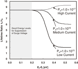
Fig. 9. Calculated relationship between trap energy level and carrier lifetime ratio (T = 300 K).
Download figure:
Standard image High-resolution imageIn other words, at low- or medium-level excess carrier densities, τc/τa is larger with deep levels than with shallow levels. At high excess carrier densities, τc/τa is smaller with deep levels than with shallow levels.
3.3. Summary
From Figs. 5 and 9, it can be seen that the surge voltage is lower at deep levels in low and medium current regions, and at shallow levels in high current regions.
Figure 10 shows the simulated dependence of the surge voltage on the current at various trap energy levels. To obtain a high current density, the diode area was reduced from that considered in the previous simulations. At 1000 A/cm2 or less, a low surge voltage is obtained with deep levels such as Et − Ei = 0.0–0.2 eV. On the other hand, at a value greater than 1000 A/cm2, the lowest surge voltage is obtained when Et − Ei = 0.4 eV. This trend matches that shown in Figs. 5 and 9. Shallow levels suppress surge voltage only when there is a very high current. Thus, deep levels such as Et − Ei = 0.0–0.2 eV are favorable for almost all power devices.
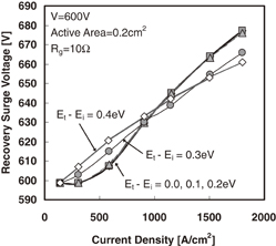
Fig. 10. Simulated dependence of recovery surge voltage with various trap energy levels (T = 300 K).
Download figure:
Standard image High-resolution imageThe effect of surge reduction on power efficiency is not very large. However, the gate resistance of IGBT can be small because of surge reduction. Figure 11 shows the simulated relationship of the IGBT turn-on loss plus the diode recovery loss and trap energy levels at 550 A/cm2. The gate resistance was adjusted to coincide with the surge voltage. The turn-on loss can be suppressed by decreasing the gate resistance. In the case where the surge voltage was maintained constant by adjusting the gate resistance, the energy loss decreased with deep levels.
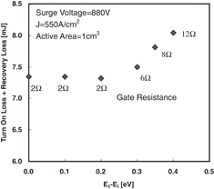
Fig. 11. Simulated relationship between IGBT turn on loss plus diode recovery loss and trap energy levels at constant surge voltage by adjusting gate resistance (T = 300 K).
Download figure:
Standard image High-resolution imageTherefore, deep levels can suppress the surge voltage and energy loss. However, these deep levels produce high leak currents. In other words, there is a trade-off between the surge voltage and the leak current.
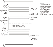
Figure 12 shows a pattern diagram of trap energy levels created by irradiating charged particles such as electrons, protons, and helium ions.30–36) This diagram shows that VV(—/0), VP, V2H, and V2O(—/0) satisfy the condition Et − Ei < 0.2 eV. For surge voltage suppression, these irradiation techniques are effective. In addition, the effect of trap energy level can be controlled by adjusting the ratio of two trap concentrations. The trap energy level obtained from two trap energy levels serves as the intermediate level. In the case of charged particle irradiation techniques, the ratio of deep levels VV(—/0) to shallow levels VO(—/0) can be controlled using the annealing time, oxide concentration, and irradiation energy.30,32) Therefore, these techniques can also adjust the trade-off between the surge voltage and the leak current.
Fig. 12. Diagram of trap energy levels created by local lifetime control in silicon.
Download figure:
Standard image High-resolution image
4. Conclusions
The effects of the trap energy levels created by localizing traps at the anode side on surge voltage were investigated in silicon power diodes. It was found that deep trap energy levels suppress surge voltage when the current density is 1000 A/cm2 or less, and that shallow trap energy levels reduce surge voltage when the current density is greater than 1000 A/cm2.