
Abstract
A proof of concept for a microwave microplasma generator that consists of a halved dielectric resonator is presented. The generator functions via leaking electric fields of the resonant modes — TE01δ and HEM12δ modes are explored. Computational results illustrate the electric fields, whereas the stability of resonance and coupling are studied experimentally. Finally, a working device is presented. This generator promises potentially wireless and low-loss operation. This device may find relevance in plasma metamaterials; each resonator may generate the plasma structures necessary to manipulate electromagnetic radiation. In particular, the all-dielectric nature of the generator will allow low-loss interaction with high-frequency (GHz–THz) waves.
Export citation and abstract BibTeX RIS

Content from this work may be used under the terms of the Creative Commons Attribution 4.0 license. Any further distribution of this work must maintain attribution to the author(s) and the title of the work, journal citation and DOI.
This article was made Open Access on 22 November 2016
Around the turn of the century, theorists began predicting what seemed like science fiction, namely, invisibility cloaks and super lenses capable of focusing beyond diffraction limits.1,2) The key to achieving such feats is the use of metamaterials, which are structures engineered for controlling permeability and permittivity. Shortly after the introduction of the theory, metamaterials were experimentally demonstrated and met with much enthusiasm.3,4) New exciting properties such as perfect absorbance were also predicted and demonstrated.5) However, current metamaterials have limitations. One prominent limitation is the small bandwidth over which metamaterials operate. As a result, many attempts have been made to produce tunable metamaterials via mechanical, electrical, or various other types of tuning.6) Plasmas became interesting candidates for metamaterials because their permittivity can be changed dynamically; this means that a plasma metamaterial can be tuned to a desired frequency. Such tunability could allow, for instance, a negative refraction over a very broad band, from GHz to THz, through changes in parameters controlling plasma properties, such as pressure, gas type, or input power.7)
In order to realize plasma metamaterials, it is necessary to generate and sustain plasmas with controlled properties and/or geometries. For instance, plasma rings and rods could be generated to replace or function with the metal structures used in earlier metamaterials.8) In 2014, split-ring resonators, previously utilized in some of the first metamaterial structures,4) were used to generate an array of plasmas, which could perhaps be used as a plasma photonic crystal/metamaterial.9,10) One may consider the previously mentioned device as an instance of a metamaterial generated by another metamaterial. However, it has also been shown that metamaterials, in this case, for negative refraction, could be made completely of dielectrics, and from this, we drew inspiration.11) Additionally, in analogy to ring resonators, it may be possible to use the resonance of dielectric resonators to tune permeability, although this possibility is not explored here.
Here, we make the first foray into all-dielectric plasma generators based on a single resonator mode for use in plasma metamaterials. It has been suggested that a high Q-factor allows for the ability to start and operate a plasma efficiently.12) Dielectric resonators can have Q-factors that are orders of magnitude larger than those of metal ring resonators, and therefore may also be valuable in generating plasmas for use in plasma metamaterials. The efficient use of energy by dielectric resonators has, in the past, made them useful as antennas at high frequencies, which suggests that these generators could be wirelessly operable.13) Unlike metals, dielectrics can have low power loss at high frequency and can have low reflectivity, which makes them suitable for low-loss interactions with GHz–THz radiation. Similar to split-ring resonators, our generator functions on the basis of sub-wavelength energy localization via a halved, dielectric resonator. Thus, the present design adds a new class of generators to the existing plasma generator flora, which are discussed in several reviews.14–19) Unlike all previous plasma generators, the all-dielectric design of our generator makes it ideal for interactions with high-frequency electromagnetic waves.
The all-dielectric plasma generators described in this paper were studied by computational and experimental methods. Computational results were obtained using the eigenmode, time-domain, and frequency-domain solvers of the commercial electromagnetic software CST Microwave Studio. Cylindrical dielectric resonators (height × diameter = 13.93 mm × 27.86 mm) composed of Zr0.8Sn0.2TiO4 were fabricated, characterized, and then halved, resulting in a plasma-generating structure (Fig. 1). The properties of the resonators and halved resonators were analyzed using an Anritsu 37369D vector network analyzer. The resonators and halved resonators were positioned in a Hakki–Coleman configuration between loop probes for magnetic coupling to the TE011 mode.20,21) To generate a plasma, the device was subjected to 2.45 GHz in a multimode microwave under ambient air conditions.
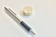
Fig. 1. A halved ZST dielectric resonator is shown here next to a pen for size comparison.
Download figure:
Standard image High-resolution imageThe concept behind the all-dielectric plasma generator is to store and leak the electric field from a resonating mode out of the dielectric and into an environment with a lower permittivity than the dielectric. The halved dielectric resonator allows the electric field of a TE01δ mode to enter air through a perpendicular interface, resulting in an increase in electric field amplitude by a factor of the permittivity of the dielectric. Recently, researchers have tried a similar approach,22) but our generator operates using a single mode instead of two, is more robust and easier to fabricate since no metallization is required or present to be degraded by the plasma, will not suffer from conductor losses, and directly benefits from the increase in electric field associated with the dielectric interface. Figure 2 was generated computationally and illustrates the TE01δ and HEM12δ modes in the cylindrical resonator (a, c) and the halved cylindrical resonator with a 100 µm gap separating the halves (b, d). The gap in the resonator does not appear to disturb the TE01δ or HEM12δ vector field's general shape in the simulation. It can be seen in Figs. 2(b) and 2(d) that the field within the air gap of the halved resonator is about 40 times greater than that in the adjacent dielectric, which corresponds to the permittivity of the dielectric. Furthermore, the models of our generator indicate that, not only do the fields in the gap increase by a factor of the permittivity (Fig. 2), but also the maximum field in the center of the gap [Fig. 3(b)] is about 15-fold larger than the field in the center of the nonsplit resonator [Fig. 3(a)], as demonstrated using the TE01δ mode. Electric fields as high as 107 V/m are achieved in simulation using a plane-wave excitation with an average incident power of 1000 W using the HEM12δ mode of a halved resonator with a 100 µm gap; the HEM12δ mode produces about 18% higher electric fields than the TE01δ mode.
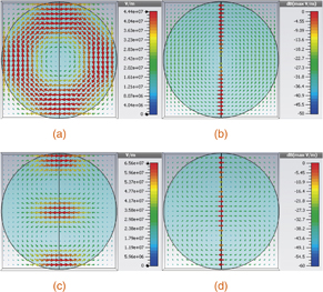
Fig. 2. (a) CST Microwave simulations of the central plane of the dielectric resonator show both the magnitude and direction of the electric field distribution of the fundamental TE01δ mode. (b) This image, also produced using CST Microwave, utilizes a dB scale in order to highlight the large increase (∼40×) in electric field magnitude in the gap of a halved resonator relative to the adjacent dielectric. (c) and (d) show the same information as (a) and (b) for the HEM12δ mode.
Download figure:
Standard image High-resolution image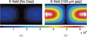
Fig. 3. (a) Simulated electric field magnitude (V/m) of the TE01δ mode in the central plane of the resonator with no gap. (b) Electric field magnitude of the TE01δ mode in the central plane of the halved resonator with gap size of 100 µm. The magnitude of the electric field in the halved resonator is increased by a factor of approximately 15 relative to the resonator with no gap.
Download figure:
Standard image High-resolution imageIn order to understand the behavior of the electromagnetic mode in the halved resonator, the fundamental (TE011) resonant frequencies of the halved resonator were studied with several gap sizes and probe angles. The gaps in the resonator were produced by inserting a shim stock between the halves of the resonator and then removing the shim stock. As shown in Fig. 4, the resonant frequency of the device increases rapidly with small (100 µm) gap changes. The error bars in the figure are based on the standard deviation from resetting the gap and remeasuring multiple times. The large error bars in the beginning (gap sizes of 0 and 0.02 mm) indicate the difficulties in producing and preventing small gaps and the device's sensitivity to small variations when utilizing small gaps. The change in resonant frequency due to gap size decreases with increasing gap distance. In particular, the trend changes markedly after 0.33 mm, and this is also near a point where the experimental results deviate from the computational results. With a 0.33 mm gap, the resonant peak in the vector network analyzer began to split into two separate peaks, suggesting the existence of two separate modes instead of one single TE011 mode, as indicated in Fig. 4. The formation of another mode at nearly the same frequency of the TE011 mode may explain the discrepancy between the experiment and the computation. At gap sizes above 0.33 mm, the resonant responses appear to be convoluted into a single peak, which is represented here as a single frequency. The optimal operating gap distance (and thus the tunability of the resonant frequency for this device) is therefore likely situated at distances greater than 0.04 mm (small error bars) and below 0.33 mm (to avoid the change in modal behavior). Figure 5 shows the Q-factors that correspond to the measurements of frequency in Fig. 4. A similar trend is seen in the Q-factor, that is, the slope begins to flatten near 0.33 mm, which is further evidence of the existence of a different mode. The Q-factor for zero gap is very similar to previously reported values of ZST using this configuration.23) The high Q-factors here suggest energy utilization much better than that of ring resonators (Q ∼ 100–300).12) Owing to losses resulting from the dielectric's contact with metal in the Hakki–Coleman setup, a technique similar to that used by the National Institute of Standards and Technology was employed for determining dielectric loss.24) Accordingly, a resonator is suspended in a metal cavity and the Q-factor of the TE01δ resonance is found to be approximately 12,000, which corresponds to a loss tangent (tan δ) of 8 × 10⁻⁵. From previous reports on ZST, one can determine similarly low loss tangents at 2 GHz (tan δ ∼ 6 × 10⁻⁵).25)
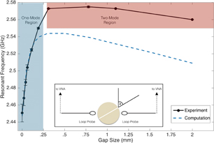
Fig. 4. Experimental and computational results of the resonant frequency of a halved resonator with various distances between the halves. Single- and double-mode regions are distinguished. Computational results show a similar trend to measurement results, especially within the first 0.25 mm. The inset of this image shows a drawing of our experimental setup looking from the top down. The resonant behavior is studied as a function of gap size and angle θ relative to the probes. Metal plates are placed above and below the resonator (not visible in the drawing).
Download figure:
Standard image High-resolution image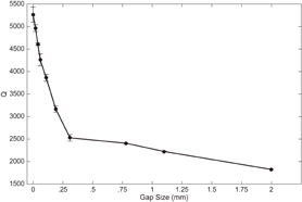
Fig. 5. The quality factor Q was measured as the gap size was varied from 0 to 2 mm. The Q-factor drops precipitously up to a gap size of about 0.3 mm, which corresponds to the two-mode region in Fig. 4. The Q-factor is determined by dividing the resonant frequency of the TE011 mode by the 3 dB bandwidth of the resonant peak when using a measurement technique developed by Hakki and Coleman and modified by Courtney.20,21)
Download figure:
Standard image High-resolution imageFigure 6 shows the variation in resonant frequency due to changes in excitation angle. That is, we rotate the device between the two probes, as shown in the inset of Fig. 4. A probe angle of zero degrees corresponds to exciting the device with the probes perpendicular to the gap. The stability of the resonant frequency with the probe angle suggests that different coupling angles do not change the response of the device. The stability of the resonant frequency denotes that the device can be predictably excited from various angles, which can be helpful in a multimode microwave cavity or when operating the device wirelessly. Since the plasma may also take on the geometry of the gap, this could allow one to orient plasma sheets as desired by rotating the halved resonators.
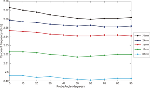
Fig. 6. The resonant frequency was measured as a function of probe angle relative to the gap (see the inset of Fig. 4 for angle definition). The resonant frequency increases with gap size, but remains relatively stable with increasing excitation angle.
Download figure:
Standard image High-resolution imageAs a final demonstration, a device was tested in a 2.45 GHz multimode microwave cavity using the dielectric resonator's HEM12δ mode, which has a free-space resonant frequency of 2.6 GHz. The device required a multimode power of 1000 W in order for the plasma to ignite in ambient air (Fig. 7), but the plasma was sustainable at 300 W, which is the minimum power of the microwave source. The breakdown strength of air is 3 MV/m, which should be exceeded by the field generated by our resonators (∼10 MV/m) at an average power of 1000 W. The extra power requirement, when comparing experimental and computational results, likely occurred owing to several factors, including the lack of a resonant frequency match, the energy input into electromagnetic modes in the microwave cavity, which may not couple well to the HEM12δ mode, and the varying dielectric properties caused by the heating of the ceramic due to high-power microwaves. Our device has an additional difficulty, that is, the gap must be set perfectly or the resonant frequency could easily vary by 5–10 MHz, as seen in Fig. 4. For this material and geometry, the loaded Q-factor also broadens in free space, which, in this case, actually helped ameliorate the problems associated with frequency matching. Many of the aforementioned problems could be rectified with a tunable microwave source.
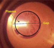
Fig. 7. Shown here is the halved dielectric resonator through a window in the microwave chamber. The resonator is circled in black and a black arrow points to the plasma formed in the gap of the resonator (marked with a black dashed line).
Download figure:
Standard image High-resolution image
In Fig. 7, the plasma is visible along with the resonator. Originally, the plasma had a purple glow, but it transitioned into an orange color. We suspect that the color change is due to the presence of impurities owing to the destruction of the ceramic. Upon excitation, the plasma appeared to cover a large fraction of the area between the resonators, and no filamentation was visible. The plasma was sustained for several minutes as the power was decreased from 1000 to 300 W. Future work will include the characterization of the plasma for this new type of generator, but we expect the plasma to be similar to previously reported capacitively coupled, microwave microplasmas, which had plasma densities and electron energies consistent with glow discharges; our models show similar expected electric field strengths (corresponding to ∼100–300 V) at similar gap sizes.12,26,27) Similarly, in a very recent study, the excitation of plasma using dual-dielectric resonators was demonstrated.28) Looking closely, one can see that our device was actually destroyed, likely due to the high microwave power typically used for microwave sintering.
We have designed, characterized, and provided a proof of concept of a new type of microwave plasma generator. We have explored properties that will help in the design of newer, finely tuned devices. This type of generator has the potential to operate very efficiently owing to high Q-factor dielectrics and the lack of conductor losses. Simulations suggest that the generator may provide high electric fields (∼105 V/m) with low power input (1 W) and even smaller losses in the dielectric, which are useful when considering an array of devices in a low-pressure argon environment. In addition, the generator can be operated wirelessly and miniaturized using high-permittivity materials. There is much room for exploration in this class of plasma generators using different geometries, materials, and modes, which may increase their viability in applications such as plasma processing, plasma transistors, plasma metamaterials, high-efficiency lamps, and so forth. Future work will include the design of new materials, plasma characterization, and different devices via the expansion of the concept.
Acknowledgments
Thanks to Eugene Furman for helpful discussions and thanks to Dinesh Agrawal and Jiping Cheng for assisting with plasma experiments. This work was supported by the Air Force Office of Scientific Research (AFOSR) under award FA9550-14-10317 through a Multi-University Research Initiative (MURI) grant titled "Plasma-Based Reconfigurable Photonic Crystals and Metamaterials" with Dr. Mitat Birkan as the program manager. Additional support is from the Applied Research Laboratory Eric Walker Fellowship Program.