

Abstract
We investigated the interface phenomena between the electrode by a low fire-through electrode paste and the silicon substrate in a crystalline silicon solar cell. Oblique polishing was used to evaluate the chemical bonding states in the depth direction. From the evaluation by X-ray photoelectron spectroscopy (XPS) and the hard X-ray photoelectron spectroscopy (HAXPES), we found changes in the chemical bonding states of Ag 3d, Si 2p, O 1s, and N 1s at the electrode–silicon interface. In addition, it was possible to confirm the reduction of Ag induced by the heat treatment at the interface. Thus, it became possible to evaluate the chemical bonding states at the interface between the electrode and the silicon substrate by adapting oblique polishing and XPS measurement.
Export citation and abstract BibTeX RIS
1. Introduction
Reduction of carrier recombination is one of the most important issues for improving the efficiency of crystalline silicon solar cells. The recombination properties in conventional solar cells are greatly improved by adopting high quality crystals and technologies such as high sheet resistance emitter, and improved front and back passivation technology including passivated emitter and rear cell (PERC) and silicon heterojunction structures.1,2) In standard p-type single crystal solar cells according to the 2015 International Roadmap for Photovoltaic (ITRPV), the bulk recombination current is 275 fA/cm2 and the surface recombination current at the front and back surfaces is 150 fA/cm2.3,4) These values are expected to be further reduced. However, a high recombination current of 549 fA/cm2 is reported at the electrode–silicon interface.5) Therefore, suppression of recombination at the interface between the electrode metal and silicon is becoming crucial in improving the conversion efficiency of next generation solar cells. The suppression can be achieved by introducing a dielectric layer between the electrode and silicon, but the trade off with increasing resistance is mandatory.6,7) This technique also requires many additional steps and is therefore still difficult to introduce into a conventional production line.
We have focused on electrode paste materials. An electrode paste comes in contact with the Si substrate by the fire-through process. Therefore, we proposed a method of improving open circuit voltage with the contact resistance kept low by suppressing the amount of fire-through with adjustment of additives in the electrode paste.8) To further optimize the electrode paste material, the fire-through process should be further refined by elucidating its mechanism. Various studies are under way for this purpose. However, there are few reports on the evaluation of the chemical bonding states at the interface between the electrode and silicon, although such evaluations should provide much information about interface phenomena.
X-ray photoelectron spectroscopy (XPS) is a typical method of evaluating the chemical bonding state. The escape depth of photoelectrons depends on their kinetic energy, and it is typically up to 5 nm from the solid surface when laboratory XPS with soft X-ray irradiation is used. Ar ion etching is used for depth direction analysis in XPS. However, in the measurement of the electrode–silicon interface in this study, there is an electrode paste of approximately 50 µm thickness on the surface and the surface is extremely rough. Therefore, it is difficult to evaluate the interface properties using the sputtering technique. We propose to adopt oblique polishing in this study. The electrode–silicon interface was exposed by performing oblique polishing. In this work, we have established an evaluation method for the electrode–silicon interface in a fire-through control electrode paste by XPS.9)
2. Experimental methods
A p-type Czochralski grown silicon (Cz-Si) wafer (3 in., mirror-polished, 10–20 Ω cm) was used as the substrate. The orientation of the substrate was selected to be (111) to simulate the textured surface with the flat surface geometry retained. A 70-nm-thick SiNx layer was deposited by plasma enhanced chemical vapor deposition (PECVD). The fire-through control silver paste was screen-printed, and the samples were fired at 775, 800, and 825 °C in atmosphere. Thereafter, oblique polishing at 0.5° was performed to expose the electrode–silicon interface using a semiautomated lapping machine (Maruto ML-150P) and an aqueous diamond slurry of nominal particles of 0.125 µm. The chemical bonding states in the SiNx films and at the electrode/silicon interfaces were investigated using a Thermo Fisher Scientific K-Alpha XPS system. The X-ray source was Al Kα with a photon energy of 1486 eV and a spot size of 0.4 mm. The inelastic mean free path and pass energy were 3.3 nm and 50 eV, respectively. Additionally, hard X-ray photoemission spectroscopy (HAXPES) was performed at the BL46XU beamline in SPring-8. By using synchrotron X-rays, we can obtain spectra from the buried interface and minimize the effect of a damaged layer induced by polishing. The take-off angle (TOA) was set to 80° to make it easy to acquire information from the buried interface.
To test the paste, n-PERT bifacial cells were fabricated. After RCA cleaning and alkaline texturing of the wafer, boron silicate glass (BSG) was deposited on the front side using atmospheric pressure CVD (APCVD). Samples were annealed (950 °C, 30 min) to obtain a P+-emitter. After removing BSG by HF etching, nondoped silicate glass (NSG) was deposited on the P+-emitter as a mask layer followed by POCl3 diffusion (850 °C, 15 min). PECVD SiNx was deposited for front and rear side passivation and anti-reflection-coating. Front and rear silver-based grid contacts were screen-printed using the fire-through control silver paste and were co-fired at 750, 775, or 800 °C.
3. Results and discussion
The XPS spectra of Ag 3d, Si 2p, and N 1s at the oblique-polished planes of a sample fired at 800 °C are shown Fig. 1. These spectra were obtained by step measurements at 378 µm intervals in the lateral direction, corresponding to 2.3 µm in the depth interval. With increasing position number from 0 to 5, the photoelectron spectra were obtained in the order of the electrode, interface, and Si substrate. The intensity of Ag 3d decreases with depth, and the decrease between positions 2 and 3 is particularly large. In the spectrum of Si 2p, the peak of the Si substrate at 99.3 eV increases as the position number increases.10–12) At position 3, a peak attributed to the Si–N bond exists at approximately 102 eV on the high energy side.10,13–15) The peak attributed to the Si–O bond can be found at approximately 103 eV at positions 4 and 5.16–18) The Si–O bond under the interfacial region at positions 4 and 5 is likely to be attributed to native oxide generated by polishing.
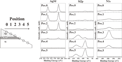
Fig. 1. Photoelectron spectra obtained by step scanning of Ag 3d, Si 2p, and N 1s from electrode to Si substrate after 800 °C firing.
Download figure:
Standard image High-resolution imageIn the spectrum of N 1s, the peak of SiNx is remarkably appearing at 397.4 eV at position 3.10,19–24) For this reason, it is considered that the SiNx passivation layer remains at the electrode/silicon interface since the fire-through control paste is used. From the above results, it was confirmed that position 3 is around the interface between the electrode and silicon.
The Ag 3d5/2 photoelectron spectra from positions 0 to 3 are shown in Fig. 2. Experimental results indicated by open circles are deconvoluted into three peaks. The pure Ag (368.0–368.3 eV), Ag2O (367.6–367.8 eV), and AgO (367.3–367.4 eV) are shown by the green, blue, and red lines, respectively.10,25–29) The cumulative fit curve is shown by the black line. The observed peak position of pure Ag is slightly lower than the peak in the literature. It might be attributed to the weak bonding of the oxygen atom to the silver atom. The peak intensity at each position is shown in Fig. 3. The peak intensities of Ag2O and AgO decrease from the electrode surface toward the interface. On the other hand, the peak of pure Ag is clearly confirmed at position 3.
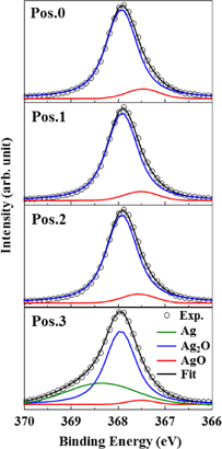
Fig. 2. Experimental results and fitting curves of the photoelectron spectra of Ag 3d5/2 from positions 0 to 3. Experimental results indicated by open circles are deconvoluted into three peaks, the pure Ag (368.0–368.3 eV), Ag2O (367.6–367.8 eV), and AgO (367.3–367.4 eV) shown by the green, blue, and red lines, respectively. The cumulative fit curve is shown by the black line.
Download figure:
Standard image High-resolution image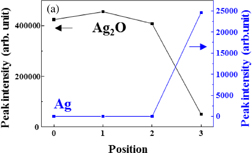
Download figure:
Standard image High-resolution image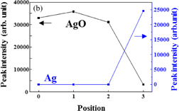
Fig. 3. Peak intensities of (a) Ag2O and (b) AgO obtained by fitting to the spectrum of Ag 3d5/2 at each position. The intensity of pure Ag is also shown in (a) and (b), corresponding to the left axis.
Download figure:
Standard image High-resolution imageSimilarly, the O 1s photoelectron spectra from positions 0 to 5 are shown in Fig. 4. The peaks indicated by the blue and red lines are attributed to SiO2 (532.5 eV) and AgOx (538.6–529.2 eV), respectively.10,30–32) Since the binding energy of AgOx gradually shifts to the high energy side as the measured position shifts from positions 0 to 5, it is conceivable that the bond between the silver atom and the oxygen atom is released at a deep position. At position 0, only the peaks corresponding to AgOx should be present, but peaks corresponding to SiOx is also confirmed. This may be due to the glass frit contained in the electrode paste.
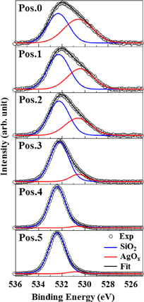
Fig. 4. Fitting for the photoelectron spectra of O 1s from positions 0 to 5. The peaks indicated by the blue and red lines are attributed to SiO2 (532.5 eV) and AgOx (538.6–529.2 eV), respectively.
Download figure:
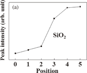
Standard image High-resolution imageThe peak intensities at all positions are shown in Fig. 5. It is confirmed that the peak intensity of SiO2 increases and that of AgOx decreases towards the Si substrate. As with the result of Ag 3d, it is possible to confirm the change in the chemical bonding states in the depth direction. By the fire-through process, it is suggested that oxygen atoms are recombined from their bonding with silver to that with silicon atoms at the electrode–silicon interface. The interface reaction may be described as follows.

The fire-through control paste was fabricated into n-PERT bifacial solar cells at firing temperature of 750, 775, and 800 °C. Current density–voltage (J–V) curves are shown in Fig. 6. Voc remains the same at 653 mV at these temperatures, whereas FF increases from 0.632 to 0.717 with firing temperature, which leads to the improvement in conversion efficiency from 16.7 to 19.0%. This result suggests that resistance loss was suppressed whereas the SiNx passivation performance was maintained.
Download figure:
Standard image High-resolution image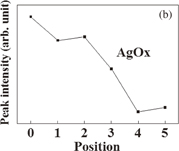
Fig. 5. Peak intensities of (a) SiO2 and (b) AgOx obtained by fitting to spectrum of O 1s at each position.
Download figure:
Standard image High-resolution image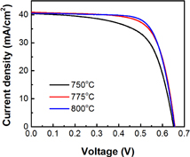
Fig. 6. J–V curves of n-PERT cells with fire-through control paste fired at 750, 775, and 800 °C.
Download figure:
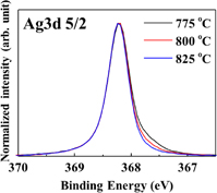
Standard image High-resolution imageSince no dependence on the heat treatment temperature was observed apparently by conventional XPS, we performed HAXPES evaluation in detail. The Ag 3d5/2 photoelectron spectra after annealing at various temperatures are shown in Fig. 7. Here, the spectra are normalized with the Ag peak intensity at a binding energy of 368.3 eV. As the annealing temperature increases, it can be confirmed that the AgO peak intensity at 367.4 eV decreases with respect to Ag2O intensity. Thus, the reduction of Ag was promoted to a greater extent as the fire-through temperature increased and more Ag atoms are possibly precipitated at the electrode–silicon interface. This phenomenon suggests that silver atoms at the electrode–silicon interface contribute to the suppression of resistance loss via electron paths.
Fig. 7. Photoelectron spectra of Ag 3d5/2 in HAXPES at various fire-through temperatures.
Download figure:
Standard image High-resolution image
4. Conclusions
In this work, we have evaluated the reduction of Ag at the interface between the paste electrode and Si in solar cell devices after the fire-through process by conventional XPS and synchrotron radiated HAXPES. As a result, we conclude that the combination of oblique polishing and photoelectron spectroscopy measurement is effective for the evaluation of bonding states at the buried interface with a thick and nonuniform overlayer in solar cells. This technique can also be applied to other interface evaluations under similar conditions such as the presence of carrier selective contacts and heterostructure interface. We believe, therefore, that the technique presents new possibilities for interface evaluation in Si solar cells and is useful for the improvement of solar cell performance.
Acknowledgments
This study was partly supported by the New Energy and Industrial Technology Development Organization (NEDO) under the Ministry of Economy, Trade and Industry. The synchrotron radiation experiments were performed at the BL46XU of SPring-8 with the approval of the Japan Synchrotron Radiation Research Institute (JASRI) (Proposal Nos. 2015A1986, 2016A1746, 2016B1872, and 2017A1782).