

Abstract
Impact of the ultralow-carbon concentration of below 1 × 10¹⁵ atoms/cm3 and thermal history on the bulk lifetime of phosphorus (P)-doped magnetic-field-applied Czochralski (MCZ) silicon was investigated. In order to accurately measure the long bulk lifetime, a direct-current photoconductive decay method was applied to a rectangular sample with a sectional area larger than 400 mm2. The measurement of an ultra-long bulk lifetime of longer than 20 ms was demonstrated using the P-doped MCZ silicon with a carbon concentration of approximately 5 × 10¹⁴ atoms/cm3. Furthermore, the bulk lifetime of MCZ silicon with shorter exposure time at 300–600 °C was extremely short; we believe that the formation behavior of the carbon-related defects in the crystal growth process affect the bulk lifetime. Therefore, not only reducing the carbon concentration but also improving the thermal history at low temperature is effective for increasing the bulk lifetime of as-grown P-doped MCZ silicon.
Export citation and abstract BibTeX RIS
1. Introduction
Large-diameter magnetic-field-applied Czochralski (MCZ) silicon with long minority carrier lifetime is required for silicon-insulated-gate bipolar transistor (IGBT) substrate as a replacement for floating zone (FZ) silicon.1,2) Increasing the minority carrier lifetime of silicon crystals is essential for improving the IGBT properties such as the on-resistance and breakdown voltage. In a recent study, we focus on reducing the carbon concentration in MCZ silicon. Higasa et al. demonstrated that reducing the carbon impurity in undoped MCZ silicon effectively increases the minority carrier lifetime.3) This indicates that the carbon impurity affects the formation of carrier recombination centers. Kishino et al. suggested that carbon impurities in silicon crystals act as heterogeneous nucleation sites for oxygen precipitates, which are the carrier recombination centers.4,5) In addition, Takano et al. reported that carbon-related complexes, such as interstitial carbon and interstitial oxygenn (CiOi), affect the collector–emitter saturation voltage, Vce(sat), of silicon-IGBT.6,7)
However, few studies have focused on the impact of reducing the carbon concentration on the minority carrier lifetime of silicon crystals. This is because conventional evaluation methods for carbon concentration in silicon crystals were incapable of detecting the carbon concentration lower than 1 × 10¹⁵ atoms/cm3, which is the practical detection limit of Fourier-transform infrared spectroscopy (FT-IR).8) Recently, a method for detecting carbon concentrations lower than 1 × 10¹⁵ atoms/cm3 in silicon crystals using photoluminescence (PL) spectroscopy was established.9,10) Using this method, the impact of reducing the carbon concentration on the minority carrier lifetime of n-type phosphorus (P)-doped MCZ silicon was investigated.
Furthermore, the thermal history during the crystal growth process is important for increasing the minority carrier lifetime. Recently, Tachibana et al. showed that the implied open circuit voltage, Voc, which is correlated with the minority carrier lifetime, is influenced by not only the carbon concentration, but also the growth condition during the crystal growth process.11) Because substitutional carbon is electrically inactive, it is considered that the thermal history during the crystal growth process affects the formation behavior of carbon-related deep-level defects. In this study, the effect of the thermal history on the minority carrier lifetime was also investigated in order to clarify the mechanism of the degradation of the minority carrier lifetime.
2. Experimental methods
2.1. Impact of sample size on bulk lifetime
The microwave-detected photoconductive decay (µ-PCD) method12) is commonly used for the measurement of minority carrier lifetime of silicon wafers. However, the µ-PCD measurement encounters difficulty in separating the bulk lifetime component from the strong surface recombination.13–15) In order to accurately measure the bulk lifetime of silicon crystals, direct-current PCD (DC-PCD; Napson HF-100DCA) designated by ASTM F28-75 and JIS H060416,17) was applied. The schematics of the DC-PCD method and rectangular-shaped samples, which were used in this study, are shown in Fig. 1. Using ohmic contacts at each end, direct current is passed through a rectangular-shaped sample with lapped surfaces. A droplet of gallium was plated on the surfaces of the two ends of rectangular samples to make ohmic contacts. The time dependence of the voltage drop across the sample is monitored after illuminating it with a short pulse of light with the near-infrared wavelength. To prevent the effect of surface recombination, a sufficiently large sample compared to the carrier diffusion length must be used.18) In this study, to measure the long bulk lifetime, the appropriate sample size that is not affected by surface recombination was investigated. Six rectangular-shaped samples with different sectional areas were cut from the same position of an 8-in. P-doped MCZ silicon ingot. The sectional area and the length of the rectangular samples used in this study are listed in Table I.
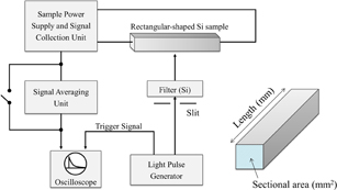
Fig. 1. Schematics of the DC-PCD method and rectangular-shaped sample.
Download figure:
Standard image High-resolution imageTable I. Sectional area and length of rectangular-shaped samples used in this study.
| Sample | Sectional area (mm2) | Length (mm) |
|---|---|---|
| 1 | 25 | 80 |
| 2 | 100 | 80 |
| 3 | 400 | 80 |
| 4 | 900 | 80 |
| 5 | 1200 | 80 |
| 6 | 1800 | 80 |
2.2. Impact of carbon concentration and thermal history on bulk lifetime
In order to investigate the impact of the carbon concentration on the bulk lifetime, several types of P-doped MCZ silicon ingots were grown. All crystals were grown to have an 8-in. diameter under a horizontal magnetic field. Commercial polycrystalline silicon feedstock was charged in a silica crucible with a 24-in. diameter. The phosphorus concentration in the crystals was maintained between 2.9 × 10¹³ and 1.6 × 10¹⁴ atoms/cm3. The carbon concentrations in the crystals were controlled by modifying the heater power and the argon gas flow rate during the melting stage.19–21) Carbon concentrations lower than 3.0 × 10¹⁵ atoms/cm3 were determined using PL spectroscopy.9,22–24) The PL measurements were conducted using a 532-nm laser as an excitation source. Chip samples were extracted from the centers of whole wafers and immersed in liquid helium in a cryostat with quartz windows. The PL from the samples was dispersed using a monochromator with a 150-groove/mm grating blazed at 1250 nm, and was detected using a cooled indium-gallium-arsenic (InGaAs) photodiode array.
The details of the samples used in this study are listed in Table II. In order to investigate the impact of thermal history, two different lengths of ingots were grown. The thermal history of these ingots during the crystal growth process is calculated using the CGSim package, which is based on the Finite Volume Method.25) Furthermore, to investigate the effect of thermal history of low temperature on the bulk lifetime, the samples were annealed individually at 300 °C in a nitrogen gas atmosphere for 3 h.
Table II. Details of the samples used in this study. The oxygen concentration was measured by FT-IR. The carbon concentration was determined by PL measurement.
| Sample | Growth condition and cut from | Oxygen concentration (atoms/cm3) | Carbon concentration (atoms/cm3) |
|---|---|---|---|
| A | Short ingot/Top | 4.0 × 10¹⁷ | 2.6 × 10¹⁴ |
| B | Short ingot/Top | 4.3 × 10¹⁷ | 2.8 × 10¹⁴ |
| C | Short ingot/Top | 4.4 × 10¹⁷ | 3.2 × 10¹⁴ |
| D | Short ingot/Top | 3.8 × 10¹⁷ | 6.6 × 10¹⁴ |
| E | Short ingot/Top | 3.9 × 10¹⁷ | 9.6 × 10¹⁴ |
| F | Short ingot/Top | 8.2 × 10¹⁷ | 4.6 × 10¹⁴ |
| G | Long ingot/Top | 4.0 × 10¹⁷ | 1.1 × 10¹⁵ |
| H | Long ingot/Top | 4.5 × 10¹⁷ | 4.5 × 10¹⁴ |
| I | Long ingot/Top | 4.8 × 10¹⁷ | 5.2 × 10¹⁴ |
| J | Long ingot/Top | 5.4 × 10¹⁷ | 7.3 × 10¹⁴ |
| K | Long ingot/Bottom | 8.5 × 10¹⁷ | 3.2 × 10¹⁵ |
3. Results and discussion
3.1. Impact of sample size on bulk lifetime
The relationship between the bulk lifetime and the sectional area of the rectangular samples is shown in Fig. 2. The bulk lifetime was a constant value of 20 ms for a sample with sectional area larger than 400 mm2. This indicates that in order to avoid the surface recombination effect, the sectional area of the rectangular sample should be larger than 400 mm2 for a bulk lifetime measurement of longer than 20 ms. For the measurement of bulk lifetimes longer than 20 ms, further experiments need to be conducted. In this study, the rectangular samples with dimension of 20 × 20 × 80 mm3 were used to accurately measure the long bulk lifetime below 20 ms.

Fig. 2. Bulk lifetime versus sectional area of the rectangular samples for n-type MCZ silicon. Bulk lifetime was measured using the DC-PCD method.
Download figure:
Standard image High-resolution image3.2. Impact of carbon concentration and thermal history on bulk lifetime
The relationship between the carbon concentration and the bulk lifetime of P-doped MCZ silicon is shown in Fig. 3. The bulk lifetimes of both the short crystal and the long crystal dramatically increased with a decrease in the carbon concentration; this indicates that the carbon-related recombination centers affect the bulk lifetime. We believe that because carbon impurities act as heterogeneous nucleation sites for oxygen precipitates, the nuclei formation of oxygen precipitates was suppressed during crystal growth by reducing the carbon concentration. Therefore, it was found that reducing the carbon concentration is crucial for increasing the bulk lifetime of P-doped MCZ silicon.
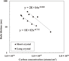
Fig. 3. Bulk lifetime versus carbon concentration for two different lengths of n-type MCZ silicon ingot. The carbon concentration is measured using PL spectroscopy. Dashed lines indicate least-squares lines.
Download figure:
Standard image High-resolution imageRegarding the effect of the thermal history during the crystal growth process, long crystal showed a longer bulk lifetime than short crystal. The comparison of the thermal history between the short crystal and the long crystal, which is calculated by CGSim, is shown in Fig. 4. This figure shows the exposure time at the top of the ingot in each temperature range during the crystal growth process. Because the short crystal experiences a shorter exposure time in the range of 300–600 °C compared to the long crystal, it was found that the thermal history at low temperature during the crystal growth process strongly affects the bulk lifetime of as-grown MCZ silicon.
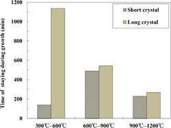
Fig. 4. Comparison of thermal history between the short crystal and long crystal calculated using CGSim for different exposure time at the top of the ingot in each temperature range.
Download figure:
Standard image High-resolution imageIn order to investigate the influence of the thermal history at low temperature on the bulk lifetime, the bulk lifetime of both the short crystal and the long crystal after heat treatment at 300 °C was evaluated. Figure 5 shows the bulk lifetime change of both the short and the long crystals after annealing at 300 °C. Although the bulk lifetime of the long crystal slightly changed before and after the 300 °C anneal, the bulk lifetime of the short crystal considerably increased after the 300 °C anneal. Because the exposure time of both the short crystal and the long crystal above 600 °C is almost the same, the defects formed in the crystals in the high temperature range is not so different. However, because the exposure time of the short crystal at 300–600 °C was considerably shorter than the long crystal, it is considered that the carbon-related defects, which were formed in the high temperature range above 600 °C during the crystal growth process, quenched and remained in the short crystal. We believe that vacancies and oxygen and substitutional carbon (VOnCs) is one of the possibilities for the carbon-related deep-level defects which are residual in the short crystal, because Higasa et al. suggested that the VOnCs that are formed after the 750 °C anneal, lead to a decrease of the bulk lifetime of as-grown MCZ silicon.3,26–29) In addition, when the heat treatment at 300 °C was conducted on the short crystal, it is believed that VOnCs changed to electrically deactivated defects such as substitutional carbon and interstitial oxygen (CsOi).30) In order to clarify the mechanism of the defects formation behavior during the crystal growth process, further experiments need to be conducted. Furthermore, in order to improve the bulk lifetime of as-grown MCZ silicon, the cooling process needs to be optimized.

Fig. 5. Bulk lifetime change of both short crystal and long crystal after 300 °C anneal. Annealing was performed in nitrogen gas for 3 h.
Download figure:
Standard image High-resolution image
4. Conclusions
Impact of the carbon concentration and the thermal history on the bulk lifetime of n-type P-doped MCZ silicon was investigated using a DC-PCD method. Two different lengths of silicon ingots were grown to change the cooling condition. First, we confirmed that in order to accurately measure a bulk lifetime longer than 20 ms, the sectional area of the rectangular sample should be larger than 400 mm2 to avoid the surface recombination effect. In the case of same cooling condition applied to both short and long crystals during the crystal growth, the bulk lifetime considerably increased with a decrease in the carbon concentration. This indicates that the carbon impurity strongly affects the bulk lifetime of P-doped MCZ silicon. Furthermore, regarding the effect of the thermal history during the crystal growth process, the long crystal showed a longer bulk lifetime than the short crystal. Because the short crystal experiences shorter exposure time at 300–600 °C compared to the long crystal, it was found that the thermal history at low temperature during the crystal growth process strongly affects the bulk lifetime of as-grown P-doped MCZ silicon. Furthermore, for the same reason, it is considered that the carbon-related deep-level defects such as CsVOn have quenched and remained in the short crystal. Therefore, in order to achieve a long bulk lifetime, it is important not only to reduce the carbon concentration, but also improve the cooling condition at low temperature during the crystal growth process. In order to clarify the mechanism of the formation behavior of carbon-related defects during the crystal growth process, further experiments need to be conducted.
Acknowledgment
This work was partly supported by the New Energy and Industrial Technology Development Organization (NEDO) under the Ministry of Economy, Trade, and Industry (METI).