
Abstract
We evaluated the compositional dependence of Pb(Mg1/3,Nb2/3)O3–PbTiO3 (PMN–PT) polycrystalline thin films by combinatorial sputtering. We prepared compositional gradient (1 − x)PMN–xPT polycrystalline thin films with preferential orientation along the 〈001〉 direction in the composition range of x = 0–0.62. We determined that the morphotropic phase boundary (MPB) composition of PMN–PT polycrystalline thin film existed at around x = 0.35, from the X-ray diffraction (XRD) measurements. The maximum value of relative dielectric constants (εr = 1498) was obtained at approximately x = 0.23. On the other hand, the piezoelectric coefficients (|e31,f| = 14.1 C/m2) peaked at the determined MPB composition of x = 0.35. From the results of the compositional dependence of dielectric and piezoelectric characteristics, the FOM ( ) of the PMN–PT (x = 0.35) thin film reached 21 GPa, which is much higher than that of the other polycrystalline piezoelectric thin films. These results suggest that PMN–PT (x = 0.35) thin film is a promising material for high-efficiency piezoelectric MEMS energy harvesters.
Export citation and abstract BibTeX RIS
1. Introduction
Piezoelectric thin films have been investigated to realize new functional micro electro-mechanical systems (MEMS), such as micro actuators, sensors or energy harvesters.1–4) It is well known that relaxor-PbTiO3 single crystals show excellent piezoelectric properties near the morphotropic phase boundary (MPB) between tetragonal and rhombohedral phases.5–7) In particular, the (1 − x)Pb(Mg1/3,Nb2/3)O3–xPbTiO3 (PMN–PT) single crystal has attracted attention because of its extraordinarily high dielectric and piezoelectric properties as well as its excellent electromechanical coupling factor.8–10) To apply PMN–PT for piezoelectric MEMS, it should be prepared in thin-film form.11–16) Baek et al. reported that (001)-oriented epitaxial PMN–PT single-crystal thin films showed extraordinary piezoelectric coefficients, e31,f = −27 C/m2, superior to those of any other thin films.15,16) On the other hand, polycrystalline thin films are easily deposited on Si substrates and useful for MEMS applications. However, there is no report on the PMN–PT polycrystalline thin film with high piezoelectricity compatible with that of single-crystal thin film.
In previous research, PMN–PT polycrystalline thin films close to the bulk MPB composition were mainly investigated. On the other hand, some researchers reported that the properties of ferroelectric thin films are different from those of bulk ceramics.17–19) In order to improve the piezoelectric properties of PMN–PT polycrystalline thin films, the precise characterization of compositional dependence is indispensable.
Combinatorial deposition is an effective method of evaluating the compositional dependence of functional films.20–22) A large number of samples with various compositions can be prepared in a single deposition process, which enables an efficient and precise optimization of film composition. In the previous work, we prepared compositional gradient Pb(Zrx,Ti1−x)O3 (PZT) thin films by sputtering and evaluated the compositional dependence to find the optimal composition ratio.23)
In this study, we applied combinatorial sputtering to the PMN–PT system and evaluated the compositional dependence of the dielectric and piezoelectric properties. We deposited compositional gradient PMN–PT thin films on Si substrates by co-sputtering of Pb(Mg1/3,Nb2/3)O3 (PMN) and PbTiO3 (PT) targets. The crystal orientation of PMN–PT polycrystalline thin film was controlled by adopting a seed layer that enhances the film growth along the 〈001〉 direction. The lattice parameters were evaluated as a function of the composition ratio to identify the MPB composition. Furthermore, the dielectric and piezoelectric properties of PMN–PT polycrystalline thin films were evaluated to find the optimal composition ratio in the PMN–PT system for piezoelectric MEMS.
2. Experimental methods
Compositional gradient PMN–PT thin films were prepared using dual-target sputtering equipment, as shown in Fig. 1. Prior to the deposition of PMN–PT films, Ti (5 nm), Pt (130 nm), and PbTiO3 (90 nm) thin films were deposited on (100) Si substrates by sputtering as the adhesion layer, bottom electrode, and seed layer, respectively. The thicknesses of PT seed layers were not only thin enough not to affect the characteristics of PMN–PT thin films, but also thick enough to control the orientation of PMN–PT thin films. PT seed layers with preferential orientation along the 〈001〉/〈100〉 direction promote the crystal growth of perovskite phase as well as control the crystal orientation of PMN–PT thin films. PMN and PT targets were mounted in the chamber and three square PT/Pt/Ti/Si substrates of 20 × 20 mm2 were placed between the two targets. The targets were simultaneously sputtered to prepare one-dimensional compositional gradient (1 − x)PMN–xPT thin films under Ar/O2 plasma at the substrate temperature of 700 °C. Figure 2 shows the compositional distribution of PMN–PT thin films deposited with applied RF power of 150 W to the PT target. The composition of the films was evaluated using an energy-dispersive X-ray spectrometer (EDX). The composition x in (1 − x)PMN–xPT is determined from Ti/(Mg+Nb+Ti). An almost linear compositional gradient in the x-direction was observed in the composition range of x from 0.21 to 0.62, and no compositional variation was observed along the y-direction. On the other hand, some compositional variations in Pb/(Mg+Nb+Ti) and Mg/Nb were observed. However their distributions were independent of sample position; therefore, in this study, we only focus on the compositional dependence of Ti/(Mg+Nb+Ti). In order to obtain a continuous compositional distribution of x in (1 − x)PMN–xPT, we conducted combinatorial sputtering deposition four times with different RF powers applied to the PT target (0, 75, 120, and 150 W). In each deposition process, the one-dimensional compositional distribution is observed. As a result, we prepared PMN–PT thin films with a composition range of x = 0–0.62, which is sufficient to evaluate compositional dependence because the MPB composition of PMN–PT bulk ceramics is x = 0.33.5) The detailed deposition conditions are listed in Table I.
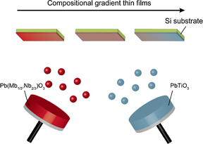
Fig. 1. Schematic illustration of deposition process for compositional gradient (1 − x)PMN–xPT thin films by combinatorial sputtering.
Download figure:
Standard image High-resolution image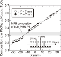
Fig. 2. Composition x in in (1 − x)Pb(Mg1/3,Nb2/3)O3−xPbTiO3 deposited with applied RF power of 150 W to the PT target as a function of position in substrates. Open and filled circles represent the measurement positions at 7 and −7 mm on the Y-axis, respectively.
Download figure:
Standard image High-resolution imageTable I. Sputtering conditions of compositional gradient (1 − x)PMN–xPT thin films.
| Target | Pb(Mg1/3,Nb2/3)O3 PbTiO3 |
| Substrate | {100}PbTiO3/Pt/Ti/Si |
| Set temperature (°C) | 700 |
| Sputtering gas (sccm) | Ar/O2 = 19.5/0.5 |
| Film thickness (µm) | 1.0–1.7 |
| RF power (W) | |
| PMN | 75 |
| PT | 0, 75, 120, 150 |
The crystal structure of PMN–PT thin films was investigated by 2θ/θ X-ray diffraction (XRD) measurements. The lattice parameters of the c-axis were calculated from the diffraction of (001) PMN–PT. Prior to the measurement of dielectric properties, we deposited a 0.3 mm diameter Pt upper electrode by sputtering and measured the capacitance and dielectric loss using an LCR meter. For the measurement of piezoelectric properties, we deposited a Pt upper electrode using a shadow mask to avoid any electrical contact with the bottom electrode, and cut out unimorph cantilevers of about 15 × 1.5 mm2 from substrates to be the length of the cantilever along the y-direction. Because the cantilever length direction was perpendicular to that of the compositional gradient, the composition of PMN–PT is almost the same in each cantilever. We applied a negative unipolar sine wave voltage from 50 to 150 kV/cm between top and bottom electrodes and measured tip displacement with a laser Doppler vibrometer. We calculated the transverse piezoelectric coefficients e31,f of PMN–PT thin films using

where h, E, δ, ν, L, and V are thickness, Young's modulus, tip displacement, Poisson's ratio, cantilever length, and applied voltage, respectively. The subscripts "p" and "s" denote the piezoelectric thin film and substrate, respectively.24) In this study, the PMN–PT thin films were not subjected to intentional poling treatments since the sputtered ferroelectric thin films such as PZT exhibited an intrinsic self-polarization toward the top electrode.25,26) Furthermore, the polarization direction of PMN–PT thin films was the same as the direction of the applied voltage during the piezoelectric measurements, and the applied electric field (50–150 kV/cm) was larger than the coercive electric field (Ec) of the PMN–PT thin films (|Ec| < 50 kV/cm along with the polarization direction).
3. Results and discussion
Figure 3 shows the XRD patterns of (1 − x)PMN–xPT thin films with the compositions of x = 0, 0.29, 0.37, 0.45, and 0.52. The diffraction patterns indicate that PMN–PT thin films with perovskite structure are preferentially oriented along the c-axis regardless of composition ratio. The lattice parameters of the c-axis are plotted in Fig. 4. The lattice parameters of PMN–PT thin films range from 4.04 to 4.10 Å and the minimum value is obtained at around x = 0.35. According to PMN–PT bulk ceramics, the lattice parameter of the c-axis is minimized at the MPB composition,27,28) suggesting the MPB composition of PMN–PT thin film was around x = 0.35, which is consistent with the MPB composition of bulk PMN–PT.5) On the other hand, the lattice parameters of PMN–PT thin films were larger than those of bulk ceramics, except for the tetragonal region, which means the crystal structure was elongated probably owing to internal stress.29) Figure 5 shows the cross-sectional scanning electron microscopy (SEM) image of PMN–PT thin film with the composition of x = 0.31, which is close to MPB composition determined from the XRD measurements. The image of PMN–PT thin film exhibits a dense columnar structure. Almost the same cross-sectional structure was observed in the PMN–PT thin films with the composition x from 0 to 0.62.
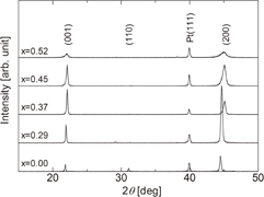
Fig. 3. XRD patterns of (1 − x)Pb(Mg1/3,Nb2/3)O3–xPbTiO3 thin films with various compositions of x = 0, 0.29, 0.37, 0.45, and 0.52.
Download figure:
Standard image High-resolution image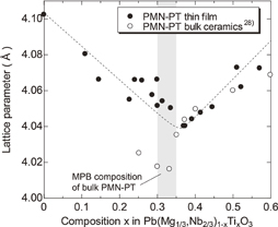
Fig. 4. Lattice parameters of c-axis as a function of composition x in (1 − x)Pb(Mg1/3,Nb2/3)O3–xPbTiO3.
Download figure:
Standard image High-resolution image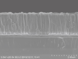
Fig. 5. Cross-sectional SEM image of PMN–PT thin film of x = 0.31, which is close to the determined MPB composition.
Download figure:
Standard image High-resolution imageWe evaluated the compositional dependence of the dielectric properties, and the relative dielectric constants (εr) and the dielectric loss are plotted in Fig. 6. The relative dielectric constants of PMN–PT thin films were in the range from 584 to 1498, and the dielectric loss was lower than 0.03. The relative dielectric constant peaks at around x = 0.23, which is shifted to the PMN-rich composition from the determined MPB composition.
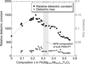
Fig. 6. Relative dielectric constants and dielectric loss of PMN–PT thin films as a function of composition x in (1 − x)Pb(Mg1/3,Nb2/3)O3–xPbTiO3.
Download figure:
Standard image High-resolution imageWe also evaluated the compositional dependence of the piezoelectric properties. Figure 7 shows piezoelectric coefficients |e31,f| as a function of composition ratio. The filled circles mean the values at the electric field of 100 kV/cm. The error bars represent the variation in |e31,f| under applied electric field from 50 to 150 kV/cm. The piezoelectric coefficients |e31,f| of PMN–PT thin films varied from 1.7 to 14.1 depending on the PMN/PT composition ratio. The maximum value of piezoelectric coefficient |e31,f| is obtained at around x = 0.35, which is consistent with the determined MPB composition. Furthermore, the curve of the compositional dependence is similar to that of bulk ceramics.28)

Fig. 7. Piezoelectric coefficients |e31,f| of PMN–PT thin films as a function of composition x in (1 − x)Pb(Mg1/3,Nb2/3)O3–xPbTiO3. The filled circles mean the values at the electric field of 100 kV/cm. The error bars represent the variation in |e31,f| under applied electric field from 50 to 150 kV/cm.
Download figure:
Standard image High-resolution imageInterestingly, the peak position of relative dielectric constant shifted to a PMN-rich composition from that of piezoelectric coefficient. We found that PMN–PT polycrystalline thin films show the highest relative dielectric constant in the rhombohedral phase. One of the possible reasons for this is that the compositional gradient PMN–PT thin films have preferential orientation along the 〈001〉 direction. It is reported that PMN–PT single crystal shows large orientation dependence of dielectric and piezoelectric properties,30) and therefore, the difference of the compositional dependence between dielectric and piezoelectric properties is attributed to the preferential orientation of PMN–PT thin films. However, a detailed investigation is required to clarify the reason behind the peak shift of the dielectric constant of PMN–PT thin films.
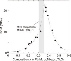
In order to determine the optimal composition of the PMN–PT system, we calculated the figure of merit (FOM) for power generation from above results. The FOM values of piezoelectric materials have been widely used in order to estimate the characteristics of vibration energy harvesters.31–33) The FOM of PMN–PT thin films could be calculated by the following equation34) and the results are plotted in Fig. 8:

where  is the dielectric constant of vacuum. The values of FOM strongly depend on the PMN/PT composition ratio, and the maximum value of 21 GPa was obtained at approximately x = 0.35. The large FOM is caused by the difference in the peak position between the compositional dependences of the relative dielectric constant and the piezoelectric coefficient. The FOM of 21 GPa is almost half that of epitaxial PMN–PT thin films (FOM = 50 GPa).15) However, it is much higher than that of the other piezoelectric thin films (ZnO = 10.3 GPa, AlN = 11.9 GPa, PZT = 6–18 GPa).31) This result indicates that 0.65PMN–0.35PT polycrystalline thin film with preferential orientation along the 〈001〉 direction is superior to other piezoelectric thin films.
Fig. 8. FOM of PMN–PT thin films as a function of composition x in (1 − x)Pb(Mg1/3,Nb2/3)O3–xPbTiO3.
Download figure:
Standard image High-resolution image
4. Conclusions
In this study, we applied combinatorial sputtering to the PMN–PT system and evaluated the compositional dependence of the dielectric and piezoelectric properties. We prepared compositional gradient (1 − x)PMN–xPT polycrystalline thin films with preferential orientation along the 〈001〉 direction in the composition range of x = 0–0.62. From the XRD measurements, the MPB composition of PMN–PT polycrystalline thin film is at approximately x = 0.35, which is almost the same as the MPB composition of bulk PMN–PT. The maximum relative dielectric constant (εr = 1498) was obtained at around x = 0.23, which is a PMN-rich composition compared with the MPB composition determined from the XRD measurements. On the other hand, the maximum piezoelectric coefficient (|e31,f| = 14.1 C/m2) was obtained at around x = 0.35, which was consistent with the determined MPB composition. The maximum FOM of the PMN–PT polycrystalline thin film was 21 GPa at around x = 0.35. This value is much higher than that of the other piezoelectric thin films. These results indicate that PMN–PT (x = 0.35) thin film is one of the promising materials for high-efficiency piezoelectric MEMS vibration energy harvesters.