Abstract
We propose a new method to determine the lateral trap position in ultra-scaled MOSFETs with a precision of less than 1 nm. The method is based on an analytical model which links the surface potential in the presence of a discrete trap to the drain voltage. We demonstrate that the dependence between the surface potential in the damaged region of the channel and the drain voltage is quasi-linear. The unique slope of this dependence corresponds to a particular lateral trap position and can thus be used as a fingerprint to locate the trap. A high accuracy is reached due to a negligibly small impact of the random dopant fluctuations on the slope magnitude. To verify our analytical approach we employ standard technology computer aided design (TCAD) methods, including random discrete dopants for both n- and p-MOSFETs with various channel lengths.
Export citation and abstract BibTeX RIS
1. Introduction
The impact of interface and oxide traps on MOSFET characteristics is crucial and still of fundamental importance.1–13) Stress induced build-up of charged defects can heavily disturb the electrostatics of a MOSFET. During device operation each trap can be charged or discharged and the kinetics of this process is defined by capture and emission times.1) This results in a local perturbation of the surface potential, and, hence, in a threshold voltage shift.1) Defects situated in different regions of the device have a different impact on the transistor performance. As such, the information about the spatial position of the trap is of great importance. Several papers devoted to the effect of the defect position on the MOSFET performance have been published so far.2–4) In some of them, however, the impact of random dopants and traps on the channel potential is not considered.2,3) Other authors mainly focus on the impact of the trap depth in the oxide.4,14) In this work we present an analytical model which demonstrates that the lateral channel position of the trap  can be extracted from the dependence between the surface potential shift in the perturbed region
  and the drain voltage
  . The impact of randomly distributed dopants, which are always present in real ultra-scaled devices,15–18) is accounted for. However, it is shown that this effect has only a negligible impact on the extraction accuracy.
2. Model description
Several papers devoted to calculation of the surface potential distribution in a MOSFET channel based on the solution of the Poisson equation have been published so far.19–22) In this work we consider n- and p-MOSFETs with a single discrete interface trap and employ an analytical expression linking the local surface potential near the trap  to the lateral trap position
  and the applied drain voltage
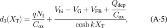
  . This problem is a particular case of the one described in Ref. 21. In this paper the MOSFET channel is divided into three region (one perturbed and the other unperturbed) and the Poisson equation is solved in each of the considered channel regions. For the device with a damaged region of any finite length the surface potential can be written as21)

where  is the gate bias,
  the flat-band voltage,
  the total charge inside the depletion layer, and
  the density of interface charges. The coefficients
  and
and  are extracted from the solution of the Poisson equation, while obtained from the boundary conditions
  is
is
where  is the dielectric constant of silicon and
  the depth of the depletion region. The geometry of the MOSFET channel including a single discrete trap at the interface is sketched in Fig. 1. In order to adjust the model21) to our particular case of extremely small perturbed area (i.e., discrete trap) we use the following assumptions:
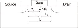
Fig. 1. Geometry of the MOSFET channel with a discrete trap at the interface.
Download figure:
Standard image High-resolution image1) The lengths of the unperturbed regions are  and
and  respectively. Here,
  is the dimension of the perturbed area, which is equal to the lateral size of the trap (typically around 0.1 nm). The distance
  is a perturbation of the second order and thus can be omitted, thereby resulting in
  .
.
2) The local surface potential corresponding to the trap position is obtained from (2.1) by setting  . For n-MOSFETs this point corresponds to the trap-induced potential minimum and for p-MOSFETs to the maximum.
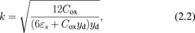
3) The following approximation is used for the coordinate dependence of depletion depth  :
:
where  and
and  are fitting parameters describing the junction depth dependence (their values are given in Table I).
Table I. The fitting parameters used in the analytical model.
| Parameter | n-MOSFET (L = 35 nm) | p-MOSFET (L = 100 nm) |
|---|---|---|
| y0 (nm) | 3.5 | 20 |
| y1 (nm) | 20 | 9 |
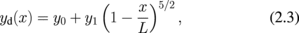
With these assumptions the surface potential in the perturbed region can be written as follows:
The relations for the coefficients  and
and  are modified as compared to the case studied in Ref. 21 according to the assumptions above (see Appendix).
Equation (2.4) links the local potential near the trap  to the trap position
  and the drain voltage
  . This means that the shape of the
  characteristics is defined by the trap position
  . This is the crucial assumption in our model because these characteristics can be simulated for different
  and used to locate the trap in the channel. Evidently, in this context it is more convenient to consider only those parts of (2.4) which depend on the drain voltage
  :
:

This equation describes the shift of the local surface potential  which is completely defined by the applied drain voltage
  for any fixed trap position
  . For example,
  for any
  . The part independent off the drain voltage
  , which is excluded from consideration at this stage, is affected by random dopant fluctuations as will be demonstrated below.
The described analytical model can be applied to devices with any channel length and doping. In order to assess the validity of our model, the results obtained will be compared with technology computer aided design (TCAD) simulations data.
3. Results and discussion
The TCAD simulations were performed on n-MOSFETs ( cm−3) and p-MOSFETs (
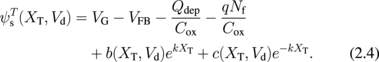
 cm−3) with channel lengths of L = 35 and 100 nm respectively. Initially, the surface potential distribution along the Si/SiO2 interface has been extracted for numerous lateral positions of discrete interface traps. The results for both n- and p-MOSFETS with three different positions of the interface traps are given in Fig. 2. The charged interface trap induces a local shift of the surface potential. The position of the potential minimum/maximum for an n-/p-MOSFET exactly corresponds to the trap position. In addition, one can see that the local surface potential shift depends on the applied drain voltage
  and that this dependence becomes stronger as the trap is shifted towards the drain.
Fig. 2. Surface potential distribution along the interface. Left: n-MOSFET, right: p-MOSFET. The insets illustrate the surface potential of the device without traps. Traps are located near the source (upper plots), in the center of the device (center plots) and close to the drain (lower plots).
Download figure:
Standard image High-resolution imageFor accurate results, the electron quantum correction potential has to be considered while modeling curves presented in Fig. 2. We use the density-gradient method23) as implemented in our device simulator Minimos-NT24) which is calibrated against our Schrödinger–Poisson solver VSP.25) This is done in order to minimize the dependence of the local surface potential near the trap  on the grid meshing.4) However, in the following discussion we will ignore the quantum corrections since it only weakly depends on the drain voltage and thus has no considerable impact on the differential
  characteristics, which are used to determine the trap position.
TCAD simulations have been performed for a case of weak inversion ( ). The trap position
  has been varied along the channel (i.e., between
  and
and  ) with a step 2–3 nm for a device with
  and 10 nm step for
  nm. For each trap position hundred different random dopant configurations have been examined and typical results for n- and p-channel devices with different trap positions are given in Fig. 3. The obtained
  characteristics have been linearly parameterized as follows:

The coefficients  and
and  as a function of
  are plotted in Fig. 4 (top), where the standard deviations due to random dopants are considered. One can see that the slope
  is practically not affected by random dopants, especially for devices with longer channel. The slope also strongly increases if the interface trap position is changed from the source towards the drain. In contrast, the extracted
  may be different for similar devices with different random dopant configurations and also symmetrical with respect to the middle of the channel, Fig. 4 (bottom). For this reason extraction of the trap position based on this characteristic appears to be problematic. Rather, only the
  -induced shift of the local surface potential
  can be used in order to determine the trap position reliably. The surface potential perturbation is

This linear behavior of  is in a good agreement with the analytical results obtained using Eq. (2.5). In Fig. 5 one can see that the
  characteristics extracted from TCAD simulations are reasonably well reproduced by those obtained with the analytical approach for both n- and p-MOSFETs with different channel lengths. The behavior of the slope
  versus
  obtained using the analytical approach is in good agreement with the simulation results given in Fig. 6. This demonstrates the soundness of our analytical model and shows that it allows to obtain the
  -dependent
  characteristics for devices with different parameters without running time consuming TCAD simulations. The abrupt growth of
  versus
  allows us to determine the trap position with very high precision. In the drain side of the channel it can reach values of less than 1 nm which is especially valuable for the characterization of traps induced by hot carrier degradation.23,26,27) It is very important that the precision of our method is not limited by the effects of random dopants, which render a practical application of some other techniques described in the literature (e.g., Ref. 3) unuseable.
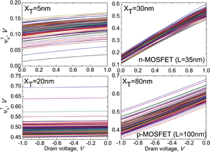
Fig. 3.  characteristics for the different trap positions. Top: n-MOSFET, bottom: p-MOSFET.
Download figure:
Standard image High-resolution image
Fig. 4. Slope (top) and intercept (bottom) of  characteristics versus
  for both devices. The impact of random dopants is illustrated.
Download figure:
Standard image High-resolution image
Fig. 5.  characteristics for different trap positions. The analytical result obtained using Eq. (2.5) are overlaid on the data extracted from TCAD and linearly fitted with Eq. (3.2). Left: n-MOSFET. Right: p-MOSFET.
Download figure:
Standard image High-resolution image
Fig. 6. Slope of  versus trap position. Analytical results are fitted with TCAD data.
Download figure:
Standard image High-resolution image
4. Possible experimental validation
Scanning probe microscopy techniques have developed rapidly during the last years and may be used to validate the proposed method experimentally. The setup for this can be realized using Kelvin probe force microscopy (KPFM) equipment28–30) with the possibility to apply  , as shown in Fig. 1 from.29) There it is assumed that the potential measurements can be performed on the edges of the device. Thus the measured profiles will contain the information about all traps situated within several nanometers into the bulk, depending on the channel doping level. For example, our TCAD simulations show that for the devices with
  cm−3 one should be able to detect the traps situated up to 2–3 nm from the edges and for
  cm−3 up to 4–5 nm. Although the potential spikes corresponding to the traps situated farther from the edges will be less pronounced, the slope of
  characteristics will be independent on the width position. One should also note that although it is rather difficult to detect the traps situated far in the bulk of the device, the characterization of near-edge traps for numerous devices will give a good statistic on the trap distribution in the corresponding set of devices.
However, the measured potential profiles may also contain the spikes induced by random dopants and it is thus very important to separate them from the ones corresponding to the traps. In order to do this one should repeat the measurements several times and see which spikes have a trap-like behavior versus time (i.e., being unstable, thereby indicating charging and discharging). Then the  dependencies have to be extracted only for those spikes which correspond to the traps. After this the background potential
  has to be subtracted in order to obtain the
  characteristics and their slope values. Finally, the slope values extracted from the experimental data have to be overlaid on similar analytical data in order to obtain
  . Note that the extraction of the lateral trap position from the
  dependencies may give a higher accuracy than the direct extraction of
  from the measured potential profiles. The reason for this is that the lateral resolution of the KPFM technique for potential measurements is typically limited to around 10 nm.28) From the other side the potential magnitudes versus
  containing all the information about the trap positions can be measured with a very high accuracy (up to several mV). Also, taking into account the simplicity of our analytical model one can simulate the similar dependencies versus the source voltage
  and measure the corresponding potential profiles. This will allow to increase the accuracy of the
  evaluation in the source side of the channel and also may be useful to solidify the results obtained using
  -dependencies.
5. Conclusions
An analytical expression linking a trap-induced surface potential shift to the applied drain voltage and trap position has been derived. The results obtained from the proposed model are in a good agreement with TCAD simulations for n- and p-MOSFETs with different channel lengths. It has been demonstrated that the lateral position of the charged interface traps in MOSFETs can be estimated precisely from the drain voltage dependence of the trap-induced surface potential shift. The main advantage of the method is that the random dopant fluctuations have only a negligibly small impact on its accuracy. The proposed method has a high potential of practical realization using modern scanning probe microscopy techniques.
Acknowledgements
The authors are thankful for the support within the FWF project No. p23958 and the EC's FP7 project No. 261868 (MORDRED).
Appendix
The coefficients  and
and  which are used in the analytical model are given by