
Abstract
We investigated the spin-dependent transport properties of strained InxGa1−xAs (x = 0.04, 0.07, and 0.16) channels grown on GaAs substrates by observing the spin-valve and Hanle signals in a lateral spin-transport device with an Fe spin source. The spin lifetime in the strained InxGa1−xAs channels estimated according to Hanle signals was one order of magnitude smaller than that in GaAs channels, and the spin lifetime depended on the degree of strain induced in the InxGa1−xAs layer. These results are explained by the strain-induced spin–orbit interaction.
Export citation and abstract BibTeX RIS
The injection and detection of spin-polarized electrons using ferromagnet/semiconductor heterojunctions has been studied extensively1–11) for creating viable spintronic devices such as spin transistors.12,13) A half-metallic ferromagnet has excellent potential as the spin source for efficient spin injection because it provides complete spin polarization at the Fermi level. Recently, we investigated the applicability of Co-based Heusler alloys to the spin injection into semiconductor channels5,7,8) as well as magnetic tunnel junctions14–17) and achieved efficient spin injection from Mn-rich Co2MnSi into GaAs via an ultrathin Co50Fe50 (CoFe) insertion layer, yielding an electron spin polarization of up to 52% at a ferromagnet/GaAs interface at 4.2 K.7) This value is more than one order of magnitude higher than that for an Fe electrode or a CoFe electrode.3)
Along with the highly efficient spin injection and detection, understanding the spin–orbit interaction (SOI) in semiconductors is an issue in the development of spintronic devices. This is because the SOI enables the generation or manipulation of the spin current even in the absence of a magnetic field and also enhances the spin relaxation in cases where electrons change their direction of motion at scattering. The influence of the SOI on the spin-dependent transport properties has been investigated electrically in an InGaAs/InAlAs two-dimensional (2D) electron gas18) and an InGaAs/InGaAsP quantum point contact19) and optically in GaAs/AlGaAs quantum wells.20,21) Recently, it was discovered by optically observing the strong SOI field in strained bulk-InGaAs channels that the strain plays a crucial role in producing a strong SOI field.22,23) Andrei and Zhang developed a strain-induced SOI model to analyze their experimental results.24) They also predicted a quantum spin Hall effect in the presence of a strain gradient.25) It is important to systematically investigate the spin-dependent transport properties of strained InGaAs channels to understand the basic physics of the quantum spin Hall effect as well as to realize spintronic devices utilizing the SOI. The purpose of our present study is to clarify the influence of the strain in InxGa1−xAs channels grown on GaAs substrates on the spin lifetime by using electrical spin injection and detection. These electrical means can be a probe to investigate the spin-relaxation mechanism in channel materials and/or device geometries that are not accessible optically, and they also represent progress toward achieving all-electrical spintronic devices.
Layer structures consisting of (from the substrate side) a 250-nm-thick undoped GaAs buffer layer, a 700-nm-thick n−-InxGa1−xAs channel layer, a 15-nm-thick n−-InxGa1−xAs → n+-GaAs transition layer, and a 15-nm-thick n+-GaAs layer were grown by molecular beam epitaxy (MBE) on semi-insulating GaAs(001) substrates. The indium compositions x were chosen to be 0, 4, 7, and 16%. The doping concentration of the n−-InxGa1−xAs channel layer was 3 × 1016 cm−3, and that of the n+-GaAs layer was 5 × 1018 cm−3, forming a narrow Schottky barrier. Samples were transferred to the second MBE chamber without exposure to air, and a 10-nm-thick Fe spin source layer and a 10-nm-thick Al cap layer were then grown at room temperature. The strains in these samples were characterized by the 2D reciprocal space mapping (RSM) of the high-resolution X-ray diffraction (XRD) from GaAs(224) and  at room temperature. The samples were then processed into lateral spin-transport devices by electron beam lithography and Ar ion milling techniques. The sizes of the injector contact and detector contact were 0.5 × 10 and 1.0 × 10 µm2, respectively, and the spacing between them was 4.0 or 8.0 µm. The spin-dependent transport properties of the lateral spin-transport devices were evaluated at 4.2 K in a four-terminal nonlocal geometry where the nonlocal voltage (VNL) between contacts 3 and 4 was measured under a constant current (I) supplied between contacts 1 and 2 at 4.2 K (Fig. 1).

Fig. 1. Schematic showing the structure of the four-terminal lateral spin-transport device and the circuit configuration for nonlocal measurement.
Download figure:
Standard image High-resolution imageFigure 2 shows a typical result for the X-ray RSM of the sample with x = 4% around the reciprocal lattice point of 224GaAs. A clear 224GaAs peak originating from the GaAs substrate and a 224InGaAs peak originating from the In0.04Ga0.96As layer were observed. The vertical dotted line indicates where the reciprocal lattice points of a fully strained layer would appear, and the inclined dotted line indicates where a completely relaxed layer would appear. Our observation of a 224InGaAs peak between these lines reveals that the In0.04Ga0.96As film prepared in this study was partially strained. A similar result was obtained for the samples with x = 7 and 16%. It is reasonable for our samples to be partially strained considering that the critical layer thickness for In0.05Ga0.95As film grown on a GaAs substrate has been reported as ∼300 nm.26) Table I presents the indium composition, lattice-relaxation rate, strain values, and mobility of the InxGa1−xAs films at 4.2 K. The lattice-relaxation rate (R) is defined as
where aInGaAs is the in-plane lattice constant of InxGa1−xAs indicated by the X-ray RSM, and aGaAs and  are the lattice constants of GaAs and completely relaxed InxGa1−xAs, respectively. The lattice-relaxation rate and absolute values of the strain-tensor components increased as x increased, with the In0.16Ga0.84As sample exhibiting the largest strain value among our samples owing to the relatively large lattice mismatch between GaAs and In0.16Ga0.84As, even though the In0.16Ga0.84As film was relaxed by 81%.

Fig. 2. Typical X-ray reciprocal mapping of In0.04Ga0.96As films grown on GaAs around the 224GaAs reciprocal lattice point.
Download figure:
Standard image High-resolution imageTable I. Summary of lattice-relaxation rate, strain-tensor components, and mobility at 4.2 K for InxGa1−xAs films with different indium compositions x.
| x (%) | Lattice relaxation rate (%) | εzz (%) | εxx (%) | εxy (%) | Mobility (cm2 V−1 s−1) |
|---|---|---|---|---|---|
| 0 | — | 0 | 0 | 0 | 2280 |
| 4 | 44 | 0.146 | −0.161 | −0.022 | 2140 |
| 7 | 58 | 0.181 | −0.198 | −0.126 | 1610 |
| 16 | 81 | 0.198 | −0.213 | 0.126 | — |
Figure 3 shows a plot of VNL/I as a function of the in-plane magnetic field for a lateral spin-transport device with x = 16%. An injection current of −125 µA was supplied, whereby the electron spins were injected from the Fe spin source to the In0.16Ga0.84As channel. The magnetic field was applied along the [110]GaAs axis direction (the shorter direction of the junction) because the easy magnetization axis for Fe epitaxially grown on GaAs was parallel to the [110]GaAs owing to the strong uniaxial magnetocrystalline anisotropy. We also observed clear spin-valve signals for devices with x = 0, 4, and 7% by applying a magnetic field parallel to the [110]GaAs direction (not shown). Similar magnetization anisotropy was observed in Co2MnSi/CoFe electrodes.5)

Fig. 3. Plot of nonlocal voltage (VNL) divided by injection current (I) with respect to the in-plane magnetic field for a lateral spin-transport device with an In0.16Ga0.84As channel.
Download figure:
Standard image High-resolution imageFigures 4(a)–4(d) plot VNL/I with respect to the out-of-plane magnetic field (Bz) in the parallel-magnetization configuration for lateral spin-transport devices with different indium compositions of 0, 4, 7, and 16%, respectively. Clear Hanle signals were observed for all the samples, demonstrating spin injection into the strained InxGa1−xAs channels. The solid lines in the figures indicate the fitting curves obtained using the spin drift-diffusion model, for which VNL/I as a function of Bz can be expressed as27)


where d is the distance between the injector and detector contacts, τ is the spin lifetime,  is the diffusion constant, lSF is the spin diffusion length, ωL is the Larmor frequency, g is an electron g factor (we assumed g-values of −0.44 for GaAs, −0.56 for In0.04Ga0.96As, −0.66 for In0.07Ga0.93As, and −0.95 for In0.16Ga0.84As28,29)), μB is the Bohr magneton, and ħ is the reduced Planck's constant. From the fitting, τ was estimated to be 16 ns for the GaAs channel, 2 ns for x = 4%, 1.4 ns for x = 7%, and 0.9 ns for x = 16%. These values are comparable to those obtained for GaAs and In0.04Ga0.96As with a doping concentration on the order of 1016 cm−3 by time-resolved Kerr rotation spectroscopy: 40 and 3 ns, respectively.23) This indicates the validity of our measurement. Interestingly, the spin lifetimes for the InxGa1−xAs channels were far shorter than that of the GaAs channel: 16 ns. Comparing the amplitude of spin-valve signal with that of a Hanle signal for x = 0.16, the former is smaller than the double of the latter. This is probably due to the imperfect formation of the anti-parallel state in the spin-valve measurement (for details, see Ref. 5).
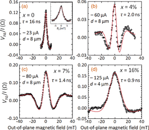
Fig. 4. Plots of VNL/I with respect to the out-of-plane magnetic field (Bz) for InxGa1−xAs channels with x = (a) 0, (b) 4, (c) 7, and (d) 16%. Space between the injector and detector contacts (d) was 8 µm for  % samples and 4 µm for the x = 16% sample. Injection currents were chosen for a junction voltage to be approximately −0.65 V. Solid lines in the figures indicate the fitting curves obtained using Eq. (2). Inset of (a) shows a Hanle signal where the low-magnetic-field region is magnified.
Download figure:
Standard image High-resolution imageFigure 5(a) shows a comparison of the bias-voltage (Vbias) dependence of the spin lifetime for different indium compositions. The estimated spin lifetime slightly decreased as |Vbias| increased for all the samples. This indicates that the electron spins injected with a higher energy tend to relax faster. One possible reason for this is that some spin scattering, such as that caused by magnon excitation, magnetic impurities, etc., was enhanced as |Vbias| increased. Another possible reason is the increase in the SOI field caused by the increase in the wave number of the injected spins as |Vbias| increased. However, further investigations are necessary to conclusively determine the origin. The spin lifetimes for the InxGa1−xAs channels were far shorter than those for the GaAs channel in all the bias regions investigated in this study. Figure 5(b) shows the indium-composition dependence of the spin lifetime (the minimum values among those measured with various bias voltages between 0 and −0.7 V for each sample are plotted). The spin lifetime sharply decreased as x increased, from τ = 16 ns at x = 0% to τ = 2.0 ns at x = 4%, and then gradually decreased as x increased to 16%. These results indicate that a spin-relaxation mechanism was strongly introduced in the strained InxGa1−xAs channels compared with the GaAs channel.

Download figure:
Standard image High-resolution image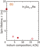
Fig. 5. (a) Injector bias-voltage dependence of spin lifetime for samples with x = 0 (closed circle), 4 (open triangle), 7 (closed square), and 16% (open diamond). (b) Indium-composition dependence of spin lifetime. The minimum values among the spin lifetimes with various bias voltages between 0 and −0.7 V for each sample are plotted.
Download figure:
Standard image High-resolution image
Next, we discuss the strong reduction of the spin lifetime in the strained InxGa1−xAs channels. Although the mobility decreased slightly as x increased, possibly owing to the increase in the alloy scattering or the degradation of the crystal quality, this does not explain the strong reduction of the spin lifetime. The relaxation of the electron spin can be generally ascribed to a randomly fluctuating magnetic field originating from (1) hyperfine interaction, (2) exchange interactions with holes, or (3) the SOI.30) We considered the contributions of each of these to the strong reduction of the spin lifetime observed in the InxGa1−xAs channels. First, the hyperfine interaction induces an effective nuclear magnetic field owing to the polarization of the nuclear spins through the transfer of the angular momentum from electron spins to nuclear spins. We recently investigated the electrical detection of the nuclear field originating from the hyperfine interaction in a Co2MnSi/CoFe/GaAs spin-injection device through oblique Hanle effect measurements.5,8) Similarly, nuclear fields of typically several tens of mT were observed in the GaAs channel of the present Fe/GaAs sample (not shown). If the hyperfine interaction is a dominant spin-relaxation mechanism in the InxGa1−xAs channels, nuclear fields comparable to or stronger than that of GaAs should be observed. However, no nuclear field was observed in the strained InxGa1−xAs channels, indicating that the hyperfine interaction is not the dominant mechanism causing the reduction of the spin lifetime. A possible reason for the absence of a nuclear field in the strained InxGa1−xAs channels is the strong reduction of the spin lifetime. Although the spin lifetime should be sufficiently long for polarized electron spins to interact with nuclei for an efficient DNP, those of the strained InxGa1−xAs channels are one order of magnitude smaller because of the spin-relaxation mechanisms other than the hyperfine interaction, yielding a negligible DNP. The exchange interactions with holes can also be excluded because we used n-type (not p-type) channels. Thus, we focus here on the effect of the SOI-induced spin relaxation. A randomly fluctuating SOI field is characterized by the strength of the SOI and the momentum relaxation time, τp. In the D'yakonov–Perel' (DP) mechanism, which is known as the major spin-relaxation mechanism in III–V semiconductors, the spin lifetime is proportional to 1/τp, that is, τ ∝ 1/τp.30) However, because the difference in τp between the GaAs channel and the In0.04Ga0.96As channel, estimated according to the Hall mobility, was only 7%, the difference in τp cannot explain the large reduction of the spin lifetime by one order. This suggests that the strength of the SOI was significantly enhanced in the InxGa1−xAs channels. The origin of the enhanced SOI was likely a strain induced in the InxGa1−xAs films rather than a difference in the bulk parameters, such as an effective mass or bandgap energy, between GaAs and InxGa1−xAs, because the latter cannot explain the strong enhancement of the SOI in the InxGa1−xAs channels. According to the strain-induced SOI model, the Hamiltonian is given by24)


where HSIA and HBIA are Hamiltonians of the structural inversion asymmetry (SIA)-type strain-induced SOI and bulk inversion asymmetry (BIA)-type strain-induced SOI, respectively; C3 and D are material constants; σx, σy, σz, are the three spin-Pauli matrices; εij ( ) represents the components of the strain tensor; and kx and ky are the wave-vector components. HSIA and HBIA have expressions similar to those of the Bychkov-Rashba and Dresselhaus SOIs,27) respectively, except for the coefficients of kx and ky. Equations (4) and (5), along with the values of the strain-tensor components for the InxGa1−xAs channels shown in Table I, suggest that the effective magnetic fields due to the strain-induced SOIs in the InxGa1−xAs channels increase as x increases and become zero in the GaAs channel because there is no strain in the GaAs channel. Therefore, this model qualitatively explains our experimental findings that the spin lifetime decreased sharply as x increased from τ = 16 ns at x = 0% to τ = 2.0 ns at x = 4% and then gradually decreased as x increased to 16%. Considering that clear Hanle signals were observed at |Bz| < 20 mT for all InxGa1−xAs channels, the effective SOI field should be comparable to or less than 20 mT, because if the effective SOI field is far larger than the external magnetic field, no Hanle precession is induced by the external magnetic field, resulting in the absence of a Hanle signal. Because the theoretical treatment of the wave number for electrons in the nonlocal geometry is not fully understood, the quantitative estimation of the SOI field using Eqs. (3) and (4) is difficult. Further theoretical and experimental investigations are necessary for the quantitative analysis.
Finally, we discuss the influence of the spin absorption from InxGa1−xAs into Fe on the spin lifetime. If the junction resistance is comparable to or smaller than the spin resistance of the channel, the spin absorption from the channel into the ferromagnet occurs, which influences the Hanle signals.31,32) The spin resistance for the InxGa1−xAs channels, estimated according to ρlSF/S, where ρ is the channel resistivity and S is the cross-sectional area of the channel, ranged from 200 to 300 Ω.33) These values are smaller by a factor of at least 20 compared with the junction resistance under all the bias conditions investigated in this study. Thus, the effect of the spin absorption was negligible.
In summary, we demonstrated spin injection into strained InxGa1−xAs channels by observing the spin-valve and Hanle signals. The results showed that the strong reduction of the spin lifetime in the InxGa1−xAs channels compared with GaAs channels primarily arises from the strain-induced SOI. All-electrical spin injection and detection can be a tool for examining the effect of the spin-relaxation mechanism and play a crucial role in the development of future semiconductor-based spintronic devices. Our findings represent progress toward achieving all-electrical spintronic devices such as spin transistors.
Acknowledgments
We thank Professor Kenji Kondo, Hokkaido University for his valuable discussion regarding the spin relaxation in semiconductors. This work was partly supported by a Grant-in-Aid for Scientific Research (JSPS KAKENHI Grant No. 25286039) and by the Japan Science and Technology Agency (JST) through its Strategic International Cooperative Program under the title "Advanced spintronic materials and transport phenomena (ASPIMATT)". T.A. was also supported by a Research Fellowship for Young Scientists from JSPS.