
Abstract
Highly conducting, optically transparent and highly bending-durable Ti-doped ZnO thin film (Ti-ZnO) on flexible Willow GlassTM via atomic layer deposition is reported. The influence of the deposited film's thickness (from 10 to 50 nm) on its microstructures, mechanical flexibility, and electrical and optical properties was investigated systematically. The results showed that the Ti-ZnO films were converted from non-crystalline structures to nanocomposite structures with increasing film thickness. The film having 40 nm thickness with enhanced optical and electrical properties showed the best figure of merit among all the films. The changes in fracture and resistivity of the films, depending on the bending cycles, showed that the films with thicknesses of 30 and 40 nm exhibited superior flexible stability. Thus, 40 nm Ti-ZnO thin film on flexible Willow GlassTM would be the best sample for efficient optical, electrical and bending properties for flexible device applications.
Export citation and abstract BibTeX RIS

Content from this work may be used under the terms of the Creative Commons Attribution 4.0 license. Any further distribution of this work must maintain attribution to the author(s) and the title of the work, journal citation and DOI.
1. Introduction
In the last decade, transparent conducting oxides (TCOs) have attracted great attention for diverse optoelectronic applications such as solar cells, light-emitting diodes, transistors, flat-panel displays and smart windows.1–3) Recently, significant research attention has been devoted to the development of TCO films on flexible substrates toward the improvement of flexible technology for advanced wearable devices.4) Existing flexible substrates including polymer materials, however, have limitations in their manufacturing processes and also in the quality of their devices, because of their low thermal stability.5) As an alternative to polymer substrates, Willow GlassTM, a flexible glass substrate, was invented by Corning Corporation. Willow GlassTM is an alkali-free alkaline-earth boro-alumino-silicate glass with 100 μm thickness.6) Thanks to its low thickness, Willow GlassTM is flexible, and also exhibits a bend stress of <100 MPa at a bend radius of 5 cm. Furthermore, Willow GlassTM has excellent thermal stability,7) which allows the fabrication of high-quality electronics and offers the possibility of manufacturing highly cost-effective and mechanically stable devices that need to be processed at high temperatures of  650 °C or to be made by roll-to-roll processing.8)
To achieve practical flexible applications, TCOs on flexible substrates should fulfill the competing demands of optical transparency in the visible region, electrical conductivity, mechanical flexibility and environmental stability.9) Indium tin oxide (ITO) shows excellent optical and electrical characteristics, but it is not an ideal TCO material with respect to low cost and mechanical flexibility.10,11) Generally, TCO film becomes fragile under mechanical bending, which can be an obstacle to flexible device application. So, researchers are seeking a cost-effective and low-fragility TCO which satisfies the requirements of flexible devices.12) Low-cost doped ZnO thin films can be implemented as an alternative to ITO,13–16) but lowering the fragility of the films toward improving mechanical flexibility is still a challenge.17–19) It is expected that the flexural strength of the film has a strong correlation with the thickness of the TCO and it can be tuned through controlling film thickness. On the other hand, the thickness of the TCO film seems to exert a significant influence on its electrical and optical properties.20) An increase in film thickness might cause a decrease in sheet resistance and film transmittance. Therefore, the effective flexibility of the TCO under bending should be achieved with preserving the enhanced optical and electrical properties.21)
Atomic-level deposition processes, which can achieve the functional properties through precise control of thickness, are highly desired. In particular, atomic layer deposition (ALD) is a powerful low-temperature growth technique which provides pinhole-free and highly conformal coating, and allows high film quality and precisely controllable composition.22–24) Thus, the ALD technique could be an efficient approach to optimizing the flexible properties of TCOs through precisely controlling atomic-scale thickness. Herein, we report the fabrication of Ti-doped ZnO films (Ti-ZnO) on flexible Willow GlassTM substrates by the ALD technique with various thicknesses (from 10 to 50 nm). The influence of film thickness on the film's microstructures and electrical, optical and flexible properties was studied systematically. Finally, superior bending durability with enhanced optical and electrical properties of the films was optimized via controlling atomic-scale precision in film thickness.
2. Experimental methods
Ti-ZnO thin films with various thicknesses ranging from 0 to 50 nm were grown on Willow GlassTM by the ALD technique. The substrate temperature was maintained at 200 °C. Diethyl-zinc (DEZ, iChems Co. Ltd.), titanium isopropoxide (TTIP, iChems Co. Ltd.) and H2O were used as the precursors of Zn, Ti, and the oxidant, respectively. To stabilize the evaporation rate of the DEZ and H2O in individual canisters, they were kept at 10 °C. Also, the temperature of TTIP was maintained at 60 °C. During the ALD process, 50 sccm N2 carrier gas was continuously supplied to the reactor. Ti-ZnO thin films were deposited by repeating a super-cycle which consisted of a TiO2 sub-cycle and a ZnO sub-cycle in sequence. For the TiO2 thin film, the sub-cycle was composed of a TTIP pulse with 50 sccm of N2 carrier gas, a purge with 50 sccm of N2, a H2O pulse for the oxidant with 50 sccm of N2 and an additional 50 sccm of N2 purge; the respective pulse times were 1 s, 7 s, 1 s and 7 s. In the case of the ZnO thin film, the sub-cycle was composed of a DEZ pulse with 50 sccm of N2 carrier gas, a purge with 50 sccm of N2, a H2O pulse for the oxidant with 50 sccm of N2 and another 50 sccm of N2 purge, where the pulse times were 1.5 s, 10 s, 1 s and 10 s, respectively. The sub-cycle ratio was 20:1 of ZnO and TiO2 for the formation of Ti-ZnO thin films.
The film thickness was measured by spectroscopic ellipsometry (J. A. Woollam Co., Inc./α-SE). The film composition was checked using Auger electron spectroscopy (AES, PerkinElmer/SAM4300). The crystalline structures of the Ti-ZnO thin films were investigated by an X-ray diffractometer (XRD, Rigaku D/MAX-2500) using Cu-Kα radiation with a 1.5405 Å wavelength, and detailed microstructures were examined by high-resolution transmission electron microscopy (HRTEM, JEOL/JEM-2100F HR). The electrical properties of the deposited Ti-ZnO thin films, such as resistivity, carrier concentration and Hall mobility, were investigated by the van der Pauw technique using a Hall-effect measurement system (Ecopia/HMS-3000). Also, sheet resistance and transmittance were obtained using a four-point probe (Advanced Instrument Technology/CMT-SR2000N) and a UV–vis spectrophotometer (Shimadzu/UV-1800), respectively. Film roughness was analyzed from an atomic force microscope (FEI/TALOS F200X). In addition, a bending test was performed using a measurement system designed in-house. The system consisted of two clamping points: the position of one point was fixed and the other clamping point could be freely located in the lateral dimension. The bending properties were measured using 2 cm × 10 cm dimensions of the Willow GlassTM sheet. The nominal radius of curvature r at the center can be given as:25)
where L is the length of the specimen, ΔL is the length between the edges of the bent specimen, and tf and ts are the thickness of the film and the substrate, respectively.
3. Results and discussion
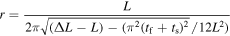
The Ti-ZnO thin films were deposited using an ALD super-cycle which consisted of a TiO2 sub-cycle and a ZnO sub-cycle in sequence as shown in Fig. 1(a). Figures 1(b) and 1(c) show the film thicknesses of ZnO and TiO2 on the Si substrate along the number of ALD cycles used for each film, indicating that the growth rates of ZnO and TiO2 thin films were 1.8 Å cycle−1 and 0.43 Å cycle−1, respectively. According to previous reports,15,26) growth rates are around 1.8–2.0 Å cycle−1 and 0.3–0.5 Å cycle−1 for the formation of ZnO and TiO2 films by DEZ/H2O and TTIP/H2O processes, respectively. The extrapolated lines go through the origin points for both thin films, which indicates that the nucleation delay of ZnO and TiO2 thin films deposited on Si by ALD was highly negligible during the deposition process.27) It is worth mentioning that the thicknesses of both ZnO and TiO2 thin films could be precisely controlled by the ALD method leading to the formation of ultrathin films. Finally, Ti-ZnO thin films were deposited with different thicknesses from 10 to 50 nm using the ALD super-cycle. To verify the uniform distribution of Ti content over the entire film matrix, AES analysis was performed, as shown in Fig. 1(d). It was found that the calculated Ti concentrations from AES spectra for all different-thickness samples are almost comparable within the film matrix.
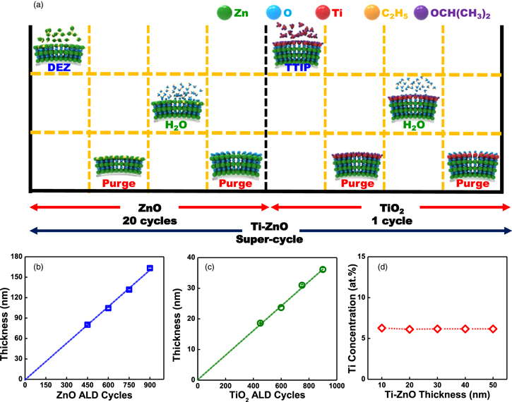
Fig. 1. (Color online) (a) Schematic of Ti-ZnO thin films based on ALD super-cycle consisting of ZnO and TiO2 sub-cycles. Dependence of film thickness of (b) ZnO and (c) TiO2 on the number of growth cycles and (d) dependence of Ti concentration on various thicknesses.
Download figure:
Standard image High-resolution imageThe XRD spectra of Ti-ZnO thin films on Willow GlassTM with different thicknesses are shown in Fig. 2(a). The Ti-ZnO thin films with thickness smaller than 30 nm exhibited non-crystalline structures without any diffraction peaks. Here, the poor crystallinity of the ZnO thin films might be due to the incomplete growth of the crystals.28) At the initial stage, growth competition could be proceeding among the neighboring shapes. After the formation of the same types of crystal faces during competition, free surfaces seem to have formed. This competitive growth mode exhibited a selective orientation. That is the reason why improved crystallinity could be observed with increasing thicknesses of the films. So, when the thickness of the Ti-ZnO thin film was increased to 40 nm, weak crystallinity started to be detected showing (101), (002) and (100) orientations, which indicate that the Ti-ZnO thin films had a wurtzite structure. As the thickness of the film increased further from 40 to 50 nm, the crystallinity increased gradually. However, at the same thickness of 50 nm, the diffraction peak of the Ti-ZnO film exhibited a significant decrease in intensity and an increase in full width at half-maximum, compared to that of the undoped ZnO thin film, which implies that the Ti-ZnO thin film had poorer crystallinity and smaller grain size (Table S1 is available online at stacks.iop.org/JJAP/58/075501/mmedia). By doping Ti onto ZnO thin films, the peak intensity of the (Ti-ZnO) thin films decreased due to the amorphous nature of the doped TiOx, and a slight shift could be observed by substituting Zn cations with Ti in the ZnO lattice.29) In addition, a difference in preferred orientations could be seen for the (100) and (002) peaks in Ti-ZnO thin films and the (002) peak in pure ZnO, which might be correlated with the change of strain due to Ti doping.30) To further elucidate the particle size and crystallinity of Ti-ZnO and undoped ZnO samples, a TEM study of 50-nm-thick samples was carried out, as shown in Figs. 2(b)–2(f). A bright-field image of an undoped ZnO sample [Fig. 2(b)] shows the presence of a ∼15 nm grain size with a polycrystalline phase as revealed by SAED and HRTEM images [inset of Fig. 2(b), Fig. 2(c)], while the Ti-ZnO film presents an amorphous-like feature with the embedment of some nanocrystals [Fig. 2(d)]. HRTEM images of the Ti-ZnO sample show an indistinct grain boundary and lattice fringes, which could be ascribed to the low crystallinity compared to that of the undoped ZnO thin film [inset of Fig. 2(d), Fig. 2(e)]. In the Ti-ZnO film, amorphous TiOx layers were incorporated into the molecular structure of ZnO, which could have led to the low crystallinity, consistent with the XRD result. TEM elemental mapping of the Ti-ZnO sample confirmed the uniform distribution of Ti within the ZnO matrix [Fig. 2(f)].
Fig. 2. (Color online) (a) XRD spectra of Ti-doped ZnO films with various thicknesses and undoped ZnO 50 nm film. (b) Bright-field TEM, (inset) SAED, and (c) HRTEM images of undoped ZnO film. (d) Bright-field TEM, (inset) SAED, (e) HRTEM and (f) TEM-EDS mapping images of Ti-ZnO film.
Download figure:
Standard image High-resolution imageThe electrical properties of the Ti-ZnO thin film were measured as a function of its thickness (Fig. 3). The resistivity of the films was found to decrease sharply with the increase of film thickness from 10 to 30 nm as depicted in Fig. 3(a). The rate of decline, however, tended to become stabilized on further increase of thickness. This might have originated from the carrier concentration of the films. To confirm the relationship, we performed carrier concentration measurement and the carrier concentration was found to increase up to a thickness of 40 nm and then tended to remain the same as shown in Fig. 3(b). According to a previous report,31) the carrier concentration could be increased when the structure of the film changes from amorphous to crystalline, where the crystallization might reduce the number of carrier traps such as defects or impurities, and thus gradually increase the free-carrier concentration. However, when the crystallinity converged on a certain level (i.e. the thickness of the film >40 nm), the corresponding variation of carrier traps could also be negligible. As a result, the changes in carrier concentration tended to be diminished as the film thickness became larger than 40 nm. Here, it is worth noting that Hall mobility increased continuously with increasing film thickness. According to the XRD patterns, crystallinity and grain size increased gradually as the thickness increased. In other words, increases in grain size and crystallinity led to the reduction of carrier scattering at the grain boundaries or impurities, and thereby finally resulted in a continuous increase of the carrier mobility. The carrier concentration of the Ti-ZnO film at 50 nm thickness was significantly higher than that of the undoped ZnO film with the same thickness of 50 nm, since the Ti4+ dopant acted as a charge carrier to make two free electrons by occupying the Zn2+ position.32) In addition, when the Ti doping concentration onto the ZnO matrix was low, the potential barrier of the grain boundary could be reduced, which would raise the enhancement of Ti-ZnO thin film mobility,33) despite the fact that the undoped ZnO had higher crystallinity and larger grain size than the Ti-ZnO film with a thickness of 50 nm.

Fig. 3. (Color online) (a) Electrical resistivity, (b) carrier concentration and Hall mobility as functions of thickness of Ti-doped ZnO films. The properties of undoped 50 nm ZnO can also be seen.
Download figure:
Standard image High-resolution imageFigure 4 shows the transmittance and figure of merit (FoM) as a function of the Ti-ZnO film thickness. Figure 4(a) shows that the transmittance of Ti-ZnO/glass decreased constantly as the film thickness increased from 10 to 50 nm. The transmittance of Ti-ZnO thin film with a thickness of 50 nm was approximately 79% (550 nm wavelength) which is similar to that of the undoped ZnO thin film with the same thickness of 50 nm. It can be confirmed that Ti doping has little influence on the transmittance of ZnO thin films. Figure 4(b) shows the FoM of all the samples for evaluation of the performance of thin films based on the optimization of their electrical and optical properties, which is given by

where T is the transmittance at the 550 nm wavelength and Rs is the sheet resistance.34) In general, the Ti-ZnO/glass samples showed higher FoM values due to lower sheet resistance compared to that of the undoped ZnO sample with a thickness of 50 nm (Fig. S1). As the thickness of the Ti-ZnO film increased from 10 to 40 nm, the FoM value increased gradually due to the sharp decrease of the sheet resistance of the film. After the highest FoM value at the thickness of 40 nm, the FoM value decreased, since the decrease rate of sheet resistance became slow while the transmittance rapidly decreased. Therefore, it could be concluded that the Ti-ZnO thin film with the thickness of 40 nm exhibited the best performance with excellent electrical and optical properties and could be one of the good candidates for TCO on Willow GlassTM.
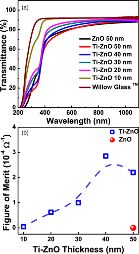
Fig. 4. (Color online) (a) Transmittance and (b) FoM of Ti-doped ZnO films with different thicknesses and undoped 50 nm ZnO film.
Download figure:
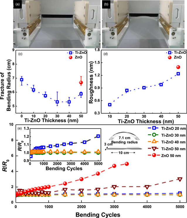
Standard image High-resolution imageIn addition, Willow GlassTM is not only flexible but also has the brittle nature of glass. Accordingly, a flexible glass could be broken by the application of hard bending pressure. As shown in Figs. 5(a) and 5(b), the fracture characteristics of Ti-ZnO film/glass were investigated with reference to those of bare Willow GlassTM (the film thickness was 0 nm and the glass was coated with ZnO film with a thickness of 50 nm). Figure 5(c) shows the bending fracture radii of the films used to evaluate the flexibility of the samples as a function of the film thickness. The samples coated with Ti-ZnO films and ZnO film exhibited smaller bending fracture radii than the bare glass. As the thickness of the Ti-ZnO thin film increased from 10 to 30 nm, the bending fracture radius decreased, reaching the lowest point and becoming comparable with that for a 40 nm thickness. In fact, many reports indicate that fracture characteristics are improved when a thin film is deposited on polymer substrates such as polyethylene naphthalate and polydimethylsiloxane by ALD.35,36) ALD thin films could seal cracks and particles on a glass surface (healing effect) which would be fracture points and thus delay fracture.37,38) However, as the thickness increased, the Ti-ZnO thin film with 50 nm thickness showed a larger bending fracture radius compared to the 30 and 40 nm films due to increased grain size (∼13 nm) which led to a further increase of surface roughness [Figs. 5(d), S2]. It is believed that larger grain size results in a weak interface between grains and would increase crack propagation rates and thereby decrease the strength of the thin film.39,40) Thus, the thickness of 50 nm showed a poor bending fracture radius compared with the other Ti-ZnO films (30 to 40 nm) due to larger grain size. The undoped ZnO thin film resulted in a greater increase of the bending radius compared to the doped ZnO film with the same thickness (50 nm) due to larger grain size (∼14.5 nm). Therefore, it can be concluded that films having grain sizes within 10 nm would show good bending properties. Moreover, the healing effect tends to saturate when the film thickness reaches a certain degree (40 nm), since a thicker film is no more effective once cracks or particles are covered (Fig. S3). The trade-off between the healing effect and film strength with the thickness determines the changes in bending fracture radius values. For successful applications of TCO/flexible glass structures, TCO durability is very important because non-optimized thickness could cause changes in electrical properties and fractures in the film. Therefore, the resistivity change rate's dependence on the bending cycles was investigated [Fig. 5(e)]. A 7.1 cm bending radius was fixed to avoid the fracture of the glass with higher bending. The result showed almost similar trends to the fracture properties. In the case of the Ti-ZnO thin film with a thickness of 10 nm, it was difficult to check the correlation due to the unstable measurement caused by higher resistivity. There was a slight resistivity change when the thickness of the Ti-ZnO thin film was 20 nm [Fig. 5(e) inset]; a stable resistivity change was observed when the thickness changed from 30 to 40 nm. After that, a change in resistivity was found in the Ti-ZnO thin film when the film thickness became 50 nm. These results can also be explained by the healing effect and thin film strength. In other words, the healing effect of covering defects for fractures and finer grains with proper strength made the Ti-ZnO films with thicknesses of 30 and 40 nm stable for resistivity maintenance during the durability test. For the undoped ZnO film, the high rates of resistivity change and fracture during the durability test are to be attributed to the bigger grain size, compared to that of the Ti-ZnO film with a thickness of 50 nm.
Fig. 5. (Color online) Photographs of Ti-ZnO film in (a) straight and (b) bending conditions. (c) Bending fracture radius as a function of Ti-ZnO film thickness. (d) Change of surface roughness and hardness of Ti-ZnO films with various thicknesses. (e) Mechanical stability test with the increase of thickness of the Ti-doped ZnO film; the inset shows a magnified image of (e). The properties of the undoped 50 nm ZnO film are also included.
Download figure:
Standard image High-resolution image
Therefore, it was observed that the 30 and 40 nm Ti-ZnO thin films showed the best flexible properties as TCO films on Willow GlassTM. In conclusion, considering the flexible, electrical and optical properties, 40 nm Ti-ZnO thin film is the most ideal for TCO application on flexible Willow GlassTM (Fig. S4).
4. Conclusions
In summary, Ti-ZnO thin films with various thicknesses (10 to 50 nm) were deposited on Willow GlassTM by ALD. Lower crystallinity, smaller grain size and lower resistivity were found for the Ti-ZnO thin films compared to a same thickness (50 nm) undoped ZnO sample. The optical transmittance of both doped and undoped samples was almost comparable in the visible region. Also, the Ti-ZnO thin films showed superior bending properties to those of the undoped ZnO film. Therefore, it is concluded that Ti doping onto ZnO thin films leads to excellent electrical, optical and bending properties. With the increase of the thicknesses of the Ti-ZnO thin films from 10 to 50 nm, the resistivity values of the films were found to decrease down to 40 nm and then almost saturate at 50 nm thickness. On the other hand, transmittance was observed to decrease constantly with increasing thickness. Therefore, the value of the figure of merit of the film with 40 nm thickness was the best among the films. For the bending durability tests, the 30- and 40-nm-thick samples showed superior stability on bending cycles. These results show that 40-nm-thick Ti-ZnO on flexible glass would be a promising TCO for realistic optoelectronic flexible applications.
Acknowledgments
This research was supported by the Global Frontier R&D Program (2013M3A6B1078874) of the Center for Hybrid Interface Materials funded by the Ministry of Science, ICT & Future Planning, Republic of Korea.