
Abstract
The InN/GaN digital alloy is a superlattice-like nanostructure formed by periodically stacking ultra-thin InN and GaN layers. In this study, we calculate the electron mobility in InN/GaN digital alloy channel high electron mobility transistors (HEMTs) by performing a single-particle Monte Carlo simulation. The results of the simulation show that alloy-induced scatterings have little impact and the electron mobility significantly improves as the effective indium mole fraction of the channel increases. This contrasts with InGaN alloy channel HEMTs, where alloy disorder and random dipole scatterings have a strong impact and the electron mobility decreases as the indium mole fraction of the channel increases.
Export citation and abstract BibTeX RIS

Content from this work may be used under the terms of the Creative Commons Attribution 4.0 license. Any further distribution of this work must maintain attribution to the author(s) and the title of the work, journal citation and DOI.
1. Introduction
Gallium nitride (GaN) and the related nitride semiconductors receive considerable attention because of their excellent properties, such as a wide bandgap, high carrier saturation velocity, and large breakdown electric field.1–5) In gallium nitride-based heterostructures such as AlGaN/GaN single heterostructures, a highly concentrated two-dimensional electron gas (2DEG) is formed at the heterointerface even in the absence of doping because of polarization charges. This enables us to realize a high-electron-mobility transistor (HEMT) for high-frequency and high-power applications.6–11)
We can expect further improvement in electron mobility by replacing the channel material of AlGaN/GaN HEMTs with InGaN because the electron effective mass of InGaN is lighter than that of GaN.3) InGaN is, however, an alloy semiconductor with a random distribution of atoms, which introduces additional scattering mechanisms such as alloy disorder12–15) and random dipole scatterings.16–18) In the previous study,19) we showed that alloy disorder and random dipole scattering have a strong impact in AlGaN/InGaN/GaN HEMTs and the electron mobility significantly decreases as the indium mole fraction of the channel increases.
Recently, Ref. 20 proposed InN/GaN digital alloy (DA) structures for optoelectronic device applications. The InN/GaN DA is a superlattice-like nanostructure formed by periodically stacking ultra-thin InN and GaN layers. Since alloy-induced scatterings are absent in a DA channel, we expect the mobility improvement by replacing the channel material of AlGaN/GaN HEMTs with InN/GaN DA structures. To evaluate what extent this improvement occurs, here, we perform a single-particle Monte Carlo simulation of the electron mobility in InN/GaN DA channel HEMTs comparing with InGaN alloy channel HEMTs.
This paper is organized as follows: in Sect. 2, we describe the method of calculating the electron mobility in DA-channel HEMTs in more detail than the original abstract (Ref. 21). Numerical results for the electronic states, scattering rates, and electron mobility are presented and discussed in Sect. 3. A conclusion is given in Sect. 4.
2. Theory
Figure 1 shows a schematic diagram of the [0001] InN/GaN DA channel HEMT considered in the present study. The InN/GaN DA channel is sandwiched between the GaN buffer layer and the Al0.27Ga0.73N barrier layer. The InN/GaN DA channel consists of 10 period of InN/GaN layers, and each InN/GaN layer consists of m-monolayer (ML) GaN and n-ML InN. The thickness of 1 ML is one half of the lattice constant c, and the m-ML GaN (n-ML InN) corresponds to m × 2.593 Å(n × 2.852 Å). We define the effective indium mole fraction as x = n/(m + n) for a InN/GaN DA consisting of periodic (GaN)m/(InN)n layers.

Fig. 1. A schematic diagram of the InN/GaN DA channel HEMT together with the coordinate axis.
Download figure:
Standard image High-resolution imageThe InN/GaN DA can be modeled either by assuming a periodic layered structure20) within an effective mass approximation (periodic layer model, PLM) or by considering the whole InN/GaN DA as a single structure whose band structure is calculated with a band structure calculation method, such as density functional theory and tight-binding (TB) method (single layer model, SLM). We adopt the latter approach (see appendix for the former approach) and the band structure of InN/GaN DA is calculated by semi-empirical tight-binding (TB) method.22–25) We use the  nearest-neighbor (NN) TB parameters of Ref. 26 for wurtzite GaN. For wurtzite InN, we performed an optimization of
  NN TB parameters to reproduce a widely accepted band structure.2) In the following calculations, we use the energy bandgap and the electron effective mass obtained from TB band structures. We obtain the energy bandgap as the energy difference between the conduction band minimum and the valence band maximum. The electron effective mass is calculated in the lowest conduction band at the Γ point. Other parameters are set to the same values as in InGaN alloy.19)
We performed single particle Monte Carlo simulation27,28) to obtain low-field 2DEG mobility of HEMTs. The calculation method was already published in detail in Ref. 19, but for the sake of completeness we will briefly describe the method in the following.
The electronic states of HEMTs along the growth direction (z direction) are calculated by self-consistently1,29–31) solving the coupled Schrödinger equation,

and Poisson equation,
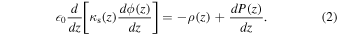
Here, n is the subband index (n = 0, 1, 2, ...), ξn(z) is the electron wave function, εn is the subband energy, ϕ(z) is the electrostatic potential, ΔEc(z) represents the conduction band discontinuity,  is the position-dependent electron effective mass, and e is the electronic charge, κs(z) is the position-dependent static dielectric constant,
  0 is the permittivity of vacuum, ρ(z) is the charge distribution, and P(z) is the polarization. The total electron energy including the in-plane (x-y plane) motion is given by

where  is the in-plane wavevector.
The scattering rates are evaluated with the obtained electronic states. We include acoustic deformation,32) polar optical phonon,33) alloy disorder, and random dipole scatterings. For the InN/GaN DA channel HEMT, we ignore alloy and random dipole scattering in the channel because the InN and GaN layers are periodically arranged.
The acoustic deformation potential scattering rate is given by33)

where

Dac is the deformation potential, ρL is the crystal density, sl is the longitudinal sound velocity, and u0(E) is the unit step function, defined by u0(E) = 1 for E ≥ 0 and u0(E) = 0 for E < 0.
The polar optical phonon scattering rate is given by

where NLO is the phonon distribution function given by

ℏωLO is the polar optical phonon energy,  is the high-frequency dielectric constant, κ0 is the low-frequency dielectric constant,
  is the in-plane phonon wavevector, and the upper (lower) symbol of ± corresponds to the phonon emission (absorption) processes. Although the polar optical phonon scattering rate in heterostructures with wurtzite crystals is different from bulk semiconductors with cubic crystals,34–36) we assume a simple cubic approximation37,38) with bulk phonon modes because it has been confirmed that it has sufficient accuracy.19)
The alloy disorder scattering rate in an alloy semiconductor AxB is given by19)

where Ω is the volume of the unit cell, VA and VB are the atomic potentials of cations A and B, respectively. We include the Thomas-Fermi dielectric function  to take into account the free-carrier screening.39,40) For the InGaN channel HEMT, the upper limit of the integration, zmax is set to the sum of the lenghs of the AlGaN barrier and InGaN channel layer. On the other hand, for the DA-channel HEMT, zmax is set to the length of the AlGaN barrier layer only because we assume that the alloy-induced scatterings absent in the DA channel. Note that z = 0 is chosen to be at the location of the surface of the AlGaN barrier layer. In the present study, we use the reported alloy disorder potential
  41) for AlGaN. For InGaN, we use
  , which is the conduction-band discontinuity ΔEc between InN and GaN.
The random dipole scattering is caused by a random distribution of dipoles in the III–V nitride alloys16,17) and its scattering rate can be written as19)

where  is the form factor given by

and  is the density of dipoles per unit cell volume. For an alloy semiconductor AxB1-xC, the dipole moments pA and pB are given respectively by17)


where Psp is the spontaneous polarization and Ppz is the piezoelectric polarization.
3. Results and discussion
Table I summarizes the parameters used in the present calculation for wurtzite GaN, AlN, and InN. For the parameters of AlGaN and InGaN alloy, such as spontaneous polarizations, piezoelectric polarizations, and energy bandgaps, we use the same values of Ref. 19. Table II shows the TB parameters used in the present calculation for wurtzite GaN and InN. The values of GaN are cited from Ref. 26, and those of InN are obtained by the optimization of the TB parameters to reproduce the reported InN band structure. For other parameters, such as the reference bond length, we use the values of Ref. 26.
Table I.
Parameters used in the present calculations for wurtzite GaN, AlN, and InN at 300 K. The listed properties are the lattice constants alc and clc, energy gap Eg, electron effective mass m*, crystal density ρL, low-frequency dielectric constant κ0, high-frequency dielectric constant  , longitudinal optical phonon energy ℏωLO, transverse optical phonon energy ℏωTO, deformation potential Dac, longitudinal sound velocity sl, and spontaneous polarization Psp.1,2,16)
| Parameters | GaN | AlN | InN |
|---|---|---|---|
| alc (Å) | 3.189 | 3.112 | 3.545 |
| clc (Å) | 5.185 | 4.982 | 5.703 |
| Eg (eV) | 3.42 | 6.28 | 0.70 |
| m* | 0.20 | 0.30 | 0.07 |

|
6150 | 3230 | 6810 |
| κ0 | 8.9 | 8.5 | 13.52 |

|
5.35 | 4.46 | 8.4 |
| ℏωLO (meV) | 92.12 | 110.35 | 72.66 |
| ℏωTO (meV) | 69.55 | 83.16 | 59.02 |
| Dac (eV) | 8.3 | 9.5 | 7.1 |

|
6.59 | 9.06 | 6.24 |

|
−0.034 | −0.090 | −0.042 |
Table II.
Parameters of the  tight-binding model for GaN 26) and InN at 300 K. The energy zero is taken at the valence-band maximum in the zincblende phase.
| GaN | InN | GaN | InN | GaN | InN | |||
|---|---|---|---|---|---|---|---|---|
| Esa | −8.937 9 | −8.344 7 | ssσ | −2.549 5 | −2.735 4 |

|
−3.907 2 | −4.869 1 |
| Esc | 4.750 1 | 2.562 6 |

|
−3.999 7 | −7.025 7 |

|
−1.225 2 | −0.901 2 |

|
28.182 4 | 30.558 1 |

|
−3.756 9 | −3.038 6 |

|
−2.096 3 | −2.914 0 |

|
35.050 7 | 34.264 1 |

|
−2.086 0 | −0.586 6 |

|
−1.755 3 | −0.647 9 |
| Epa | 2.062 6 | 1.958 4 |

|
3.921 0 | 3.349 2 |

|
−1.900 7 | −1.700 1 |
| Epc | 11.450 1 | 10.149 7 |

|
4.048 9 | 3.813 7 |

|
−1.328 6 | −1.671 0 |

|
27.943 3 | 28.468 2 |

|
4.291 1 | 4.336 4 |

|
2.276 1 | 2.198 8 |

|
28.408 8 | 26.496 9 |

|
2.086 1 | 1.204 3 |

|
3.219 5 | 3.307 0 |

|
29.409 8 | 30.683 8 |

|
4.742 9 | 4.348 8 |

|
−1.201 6 | −1.564 3 |

|
26.989 8 | 26.296 3 | ppπ | −1.430 2 | −1.375 9 | ddπ | 6.075 7 | 6.738 0 |
| ddδ | −4.443 6 | −4.991 5 |
Figure 2 shows the calculated band structures of InN using the TB parameters of Table II. The bandgap is 0.7 eV and the electron effective mass is  . Figure 3 depicts the band structures of InN/GaN DA of m = 4 and n = 1 (x = 0.2). The bandgap and effective mass for InN/GaN DAs are given in Figs. 4 and 5, respectively. In these figures, m decreases from 5 ML to 0 ML with a 1 ML step, while n increases from 0 ML to 5 ML with a 1 ML step with keeping m + n = 5. Although the band gap shows a small bowing, the effective mass almost follows Vegard's law.

Fig. 2. The  model band structures of InN at 300 K calculated with the TB parameters of Table II.
Download figure:
Standard image High-resolution image
Fig. 3. The  model band structures of InN/GaN DA. Thickness of each GaN and InN layers are m = 4 and n = 1, respectively.
Download figure:
Standard image High-resolution image
Fig. 4. The bandgap of InN/GaN DA obtained from the calculated TB band structure at 300 K as a function of the indium mole fraction.
Download figure:
Standard image High-resolution image
Fig. 5. The electron effective mass of InN/GaN DA obtained from the calculated TB band structure at 300 K as a function of the indium mole fraction.
Download figure:
Standard image High-resolution imageFigure 6 shows the electronic states obtained by the self-consistent calculation at T = 300 K for a DA-channel HEMT of m = 4 and n = 1 (x = 0.2). The 2DEG density is found to be NDA = 1. 04 × 1013 cm−2 which is almost the same as the 2DEG density of an InGaN alloy channel HEMT of x = 0.2, i.e.,  (see Fig. 7).
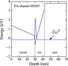
Fig. 6. (Color online) Calculated conduction band edge profile and spatial probability distribution  of the lowest subband along the c-axis slice of an InN/GaN DA channel HEMT of m = 4 and n = 1 (x = 0.2).
Download figure:
Standard image High-resolution image
Fig. 7. (Color online) The same as Fig. 6 but for an InGaN alloy channel HEMT of x = 0.2.
Download figure:
Standard image High-resolution imageFigure 8 and 9 show the calculated scattering rates of the 2DEG in the DA- and InGaN-channel HEMTs, respectively. For the InGaN-channel HEMT, the alloy disorder and random dipole scatterings are the dominant scattering mechanisms. On the other hand, for the DA-channel HEMT, those alloy-induced scatterings have small impact on 2DEG. This can be attributed to the fact that the alloy-induced scatterings are absent in the DA channel region and the electron penetration into the AlGaN barrier layer is small (see Fig. 6). As for the phonon scatterings, the acoustic deformation potential and polar optical phonon scattering rates are almost the same between DA- and InGaN-channel HEMTs because of the small difference in the spatial distribution of 2DEGs in these HEMTs.

Fig. 8. Acoustic deformation, polar optical, alloy disorder, and random dipole scattering rates at 300 K for electrons in the lowest subband in the InN/GaN DA channel HEMT of m = 4 and n = 1 (x = 0.2) as a function of the electron energy. Zero energy is set to be the Fermi level. 10 subbands are included in the calculation.
Download figure:
Standard image High-resolution image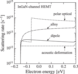
Fig. 9. The same as Fig. 6 but for the InGaN alloy channel HEMT of x = 0.2.
Download figure:
Standard image High-resolution imageFigure 10 shows the 2DEG mobility μ as a function of the indium mole fraction x of the channel, obtained by single-particle Monte Carlo simulation under a uniform electric field of  . Open squares show the mobility of InGaN alloy channel HEMTs, μalloy, and closed circles show the mobility of InN/GaN DA channel HEMTs within the single layer model (SLM), μSLM. In Fig. 10, we also plot the mobility of InN/GaN DA channel HEMTs within the periodic layer model (PLM), μPLM for comparison (see Appendix for PLM). Note that the marks at x = 0 represent the results for the GaN-channel HEMT. For the InGaN alloy channel HEMT, alloy disorder and random dipole scatterings have a strong impact and 2DEG mobility μ decreases as x increases, i.e.,
  when x = 0.2, and
  when x = 0.4. In contrast, for the DA channel HEMT, those alloy-induced scatterings have little impact and μ improves significantly as x increases, i.e.,
  = 1,800
  (
( = 1,900
  ) when x = 0.2, and
  = 2,100
  (
( =
=  ) when x = 0.4.

Fig. 10. Dependence of 2DEG mobility on indium mole fraction x at T = 300 K. Open squares show the mobility of InGaN alloy channel HEMTs. Closed (open) circles show the mobility of InN/GaN DA channel HEMTs within the single (periodic) layer model.
Download figure:
Standard image High-resolution image4. Conclusions
We investigated the 2DEG mobility in InN/GaN DA channel HEMTs compared with InGaN alloy channel HEMTs. We find that alloy-induced scatterings have little impact and the electron mobility significantly improves as the effective indium mole fraction of the channel increases in InN/GaN DA channel HEMTs.
Acknowledgments
This work was supported in part by MEXT of Japan as a social and scientific priority issue (Creation of new functional devices and high-performance materials to support next-generation industries; CDMSI) to be tackled by using post-K computer, and by MEXT Grant-in-Aid for Scientific Research on Innovative Areas "Science of hybrid quantum systems".
Appendix
In this appendix, we present the Monte Carlo results within a periodic layer model (PLM). For the single layer model (SLM) as discussed in the main text, a DA channel is considered as a single material described with a single band-structure. For PLM, we solve the Schrödinger equation with a periodic potential profile assuming that each layer can be described with its band-structure, and obtain the electronic states. The obtained electronic states of InN/GaN DA channel HEMT are shown in Fig. A·1, in which we find that the 2DEG density is  .
.

Fig. A·1. (Color online) The same as Fig. 6 but for the PLM of m = 4 and n = 1 (x = 0.2).
Download figure:
Standard image High-resolution imageFigure A·2 shows the calculated scattering rates of a DA channel HEMT within the PLM. Note that, in this calculation, the electron effective mass of InN/GaN DA are assumed to be the same as that of InGaN alloy with a small bowing:33)

with  , and b = − 0.07 m0. We see that the effect of the alloy scattering is smaller than that in the SLM [see Fig. 8]. This is because the penetration rate of the electrons into the AlGaN barrier layer is 5.4 % in the PLM, which is smaller than 10.6 % in the SLM (see also Fig. 6). On the other hand, the polar optical phonon scattering rate at the bottom of the lowest subband, which is the dominant scattering mechanism, is almost the same as in the SLM, i.e.,
  and
and  .
.

Fig. A·2. The same as Fig. 8 but for the PLM of m = 4 and n = 1 (x = 0.2).
Download figure:
Standard image High-resolution image
Figure 10 shows a comparison of the 2DEG mobilities of the PLM and SLM. We see that the mobility of the PLM is slightly higher than that of the SLM. This is mainly because the electron effective mass of InGaN alloy used in the PLM is slightly smaller than that of the SLM, while the phonon scattering rates are almost the same with each other.