
Abstract
We propose a fabrication process for a silicon on insulator (SOI) wafer with a diamond buried oxide (BOX) layer by combining nanodiamond-seeding deposition and a surface-activated bonding technique for high-frequency and power device applications. The diamond layer was deposited on a base wafer by the spin-coating of nanodiamonds and microwave-plasma-enhanced chemical vapor deposition. The thermal conductivity of this deposited diamond layer was three times that of a conventional SiO2 layer. A silicon wafer was then bonded to the diamond layer at room temperature in ultrahigh vacuum without forming any voids. Additionally, this SOI wafer was used to fabricate devices at 1000 °C. Therefore, we believe that this SOI wafer with a diamond BOX layer and its fabrication process are important for the realization of self-heating devices such as next-generation high-frequency and power devices.
Export citation and abstract BibTeX RIS

Content from this work may be used under the terms of the Creative Commons Attribution 4.0 license. Any further distribution of this work must maintain attribution to the author(s) and the title of the work, journal citation and DOI.
1. Introduction
High-frequency devices have been widely used in wireless communication applications such as smartphones, tablets, high-definition multimedia interfaces, and automobiles.1–3) To counter global warming, low CO2 emissions are necessary. For example, automobiles have been changing from gasoline-based to hybrid electric and fully electric vehicles. These automobiles are manufactured using various power devices.4,5) High-frequency and power devices have mostly been fabricated using silicon on insulator (SOI) wafers.6,7) Such devices are surrounded by SiO2, a buried oxide (BOX) layer, and shallow trench isolation.8) Because SiO2 has low heat conductivity, these devices are self-heating.9) Thus, the electrical characteristics of the devices degrade, lowering their performance. To resolve this technical issue, the BOX layer should be changed from SiO2 to an alternative material with sufficient thermal conductivity.
High-frequency and power devices are fabricated in a silicon layer on a BOX layer of a base wafer. It is important for the silicon layer to have no metallic impurities. However, it takes a few hours to bond a silicon wafer (layer) to a BOX layer above 800 °C.10) Because it takes a long time to fabricate an SOI wafer at a high-temperature using this method, contamination with metallic impurities occurs during fabrication, incurring a high cost and resulting in additional problems. Therefore, we propose a fabrication process for an SOI wafer that has thermal conductivity for high-frequency and power devices. The BOX layer is made of diamond, and the silicon wafer (layer) is bonded to the diamond layer using a surface-activated bonding (SAB) technique11,12) at room temperature in ultrahigh vacuum for a short time. Because the silicon wafer (layer) is bonded to the BOX layer at a low temperature for a short time, there is no thermal stress or metallic impurity contamination.
When a diamond layer is grown on a substrate not made of diamond, a seed must be introduced into the substrate surface. There are two types of seeding methods. One involves scratching the substrate using diamond powder with a grain size of 100 nm–10 μm.13) The other method involves implanting carbon ions into the substrate by applying a voltage to the substrate in a deposition chamber using bias-enhanced nucleation (BEN).14) Because the scratching method produces many scratches on the silicon wafer surface, it may decrease the substrate strength. This method does not stably generate nucleation centers over the entire surface of the silicon wafer substrate.15,16) The BEN method damages the surface of a substrate, such as a single-crystal silicon substrate, owing to ion implantation,17,18) resulting in a bent wafer19,20) and an insufficient nucleation-center density.21,22) The deposition equipment used in BEN is also very complex and expensive.23) Thus, a fabrication method that does not damage the silicon substrate or require expensive processing equipment is necessary. Such a fabrication method involves the spin-coating of diamonds of under 10 nm (nanodiamonds) dissolved in water on a silicon substrate. Because this spin-coating method is used in photolithography as a device fabrication process,24) it is very reasonable and can be used to form nucleation centers over the entire silicon wafer surface.
There are two types of diamond deposition method. One type is microwave-plasma-enhanced chemical vapor deposition (MW-CVD),25,26) and the other is hot-filament-type CVD (HF-CVD),27,28) which is a thermal CVD process. HF-CVD can be used to deposit diamonds on a wide substrate. Thus, we consider that diamonds can be deposited on a 12 inch silicon wafer by a combination of nanodiamond-coating seeding and HF-CVD. Therefore, we believe that an SOI wafer with a diamond BOX layer and its fabrication process are important for the realization of self-heating devices such as high-frequency and power devices.
2. Experimental methods
The fabrication process of our SOI wafer with a diamond-BOX layer is shown in Fig. 1. We fabricated two silicon wafers: a base wafer and a bonding wafer. The base wafer was coated with nanodiamonds by spin-coating. After baking the base wafer, the diamond layer was deposited on the base wafer by MW-CVD. The top surface of this diamond layer was polished by chemical mechanical polishing (CMP). Then, the bonding wafer was bonded to the diamond layer by SAB at room temperature in ultrahigh vacuum. Finally, the bonding wafer was ground and polished until a silicon layer was formed on the back side as the active layer of the device, which is opposite the wafer-bonding interface.
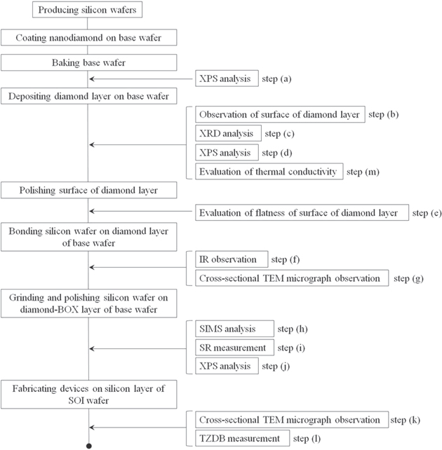
Fig. 1. Experimental flow. Steps (a), (d), and (j): evaluation of bonding elements, step (c): evaluation of crystalline nature of diamond layer, step (e): evaluation of flatness of diamond layer surface, step (f): IR observation, steps (g) and (k): cross-sectional TEM micrograph observation, steps (h) and (i): SIMS analysis and SR measurement of silicon layer, step (l): TZDB measurement, and step (m): evaluation of thermal conductivity.
Download figure:
Standard image High-resolution image2.1. Sample preparation
We used (100) Czochralski (CZ) 2 inch silicon wafers. The base wafer was polished to 3 mm thickness and the bonding wafer, used as a silicon layer, was polished to 500 μm thickness. When another material layer is deposited on a base wafer, the base wafer might be warped. Thus, we used base wafers that were thicker than standard wafers. These wafers were made of phosphorus-doped CZ-silicon single-crystal. Their resistivity was 5 Ω cm and their oxygen concentration was 1.2 × 10⁻¹⁸ atoms cm−3. As shown in Fig. 1, the base wafer was coated with nanodiamonds dissolved in water by spin-coating. The grain size of these nanodiamonds was under 10 nm, and they made up 5% of the wafer. This coated base wafer was baked at 80 °C for 3 min in air in a clean room using a hot plate. Then, a diamond layer was deposited as a BOX layer on the base wafer between 900 °C and 1200 °C using MW-CVD (Nihon Koshuha Co. Ltd, MDD-2016). Only the top surface of this diamond layer was polished by CMP. The bonding wafer was then bonded to the polished diamond layer by SAB at room temperature in ultrahigh vacuum under 1 × 10⁻⁵ Pa by connecting the dangling bonds on the surfaces of the two wafers (Mitsubishi Heavy Industries Machine Tool Co. Ltd, MWB-08-AX). These dangling bonds were formed on the top surface of the two wafers by irradiating argon ions at 1–2 keV to activate the surface of the two wafers. After bonding the two wafers, the bonded wafer was ground and polished until a silicon layer of 2 μm formed on the back side, which is opposite the wafer-bonding interface. A reference SOI wafer was fabricated using thermal oxidation and thermal bonding. A 1.5 μm BOX layer was formed on the base wafer by thermal oxidation above 900 °C. The bonding wafer was bonded to the BOX layer of the base wafer by high-temperature treatment at 800 °C for 2 h and 1150 °C for 1 h.10)
2.2. Experimental procedure
As shown in Fig. 1, we analyzed how binding occurred on the surface of the nanodiamond-coated base wafer after baking [step (a)]. We then observed and analyzed the diamond layer after deposition and polishing [steps (b)–(e)]. Next, we looked for voids after bonding the silicon wafer to the diamond layer [steps (f) and (g)]. Then, we evaluated the concentration of doping elements and the resistivity in the silicon layer and analyzed the diamond layer after grinding and polishing the bonding silicon wafer to the thickness of the active layer of the device [steps (h)–(j)]. After that, we evaluated the breakdown electric field of the diamond layer after fabricating actual devices in the silicon layer [steps (k) and (l)]. Finally, we evaluated the thermal conductivity of the diamond layer on the base wafer [step (m)].
2.2.1. Analysis of base wafer surface after baking nanodiamond-coated base wafer and depositing diamond layer on base wafer
We analyzed the surface of samples after baking the nanodiamond-coated base wafer and depositing a diamond layer on the base wafer by X-ray photoelectron spectroscopy (XPS). The XPS analysis equipment we used comprised a Quantera SXM spectrometer (ULVAC-PHI) for the baked nanodiamond-coated wafer and an ESCALAB-220iXL spectrometer (Thermo Fisher Scientific) for the diamond layer-deposited base wafer. The X-ray used in this analysis was the monochromatic Al Kα1,2 line at 1486.6 eV, where the area of the analysis regions were 1 × 104 μm−2 for the baked nanodiamond-coated wafer and 1 mm2 for the diamond layer-deposited base wafer, and the angles of photoelectron detection were 45° for the baked nanodiamond-coated base wafer and 90° for the diamond layer-deposited base wafer.
2.2.2. Analysis of crystalline nature of diamond layer deposited on base wafer
We analyzed the surface of another base wafer by X-ray diffraction (XRD) using a SmartLab diffractometer (Rigaku) after depositing a diamond layer on the wafer. The X-ray used in this analysis was the graphite-monochromatic Cu Kα line at 8047.8 eV, and the angles of photoelectron detection were 10°–150° for the studied sample.
2.2.3. Observation of surface and cross section of studied sample
We used an OPTIPHOT-88 microscope (Nikon) for optical microscopy (OM) observation and an H9000UHR-I microscope (Hitachi) for transmission electron microscopy (TEM) observation to observe the diamond layer surface and wafer-bonding-induced defects, respectively. The OM observation was performed to characterize the grain size of the polycrystalline diamonds after depositing them on the base wafer and polishing the surface of the diamond layer. Cross-sectional TEM and high-resolution TEM (HR-TEM) micrographs were used to characterize structural defects, such as wafer-bonding-induced defects, during the fabrication of the bonding wafer.
2.2.4. Evaluation of roughness of surface of polished diamond layer of base wafer
We evaluated the roughness of the top surface of the diamond layer on the base wafer after polishing the surface of the diamond layer. We used a Dimension Icon atomic force microscope (AFM) (Bruker) to evaluate the roughness.
2.2.5. Evaluation of voids after bonding silicon wafer to diamond layer of base wafer
We evaluated the voids after bonding the silicon wafer to the diamond layer by SAB at room temperature in ultrahigh vacuum using the infrared-transmission (IR) observation method. An IRise (Moritex) system was used for the IR observation. In this method, voids are detected using IR radiation, which is transmitted through the silicon wafer and reflected at voids. The wavelength of the radiation was over 1000 nm.
2.2.6. Evaluation of depth profile of concentration for doping element in silicon layer after fabricating SOI wafer
The phosphorus concentration was measured by secondary ion mass spectroscopy (SIMS) analysis using an IMS7f device (CAMECA). After fabricating the SOI wafer, small pieces were cut from the wafer for SIMS analysis. The phosphorus concentration about 2 μm below the wafer surface was estimated from the intensity of the impurity-related SIMS peaks in the SIMS spectra.
2.2.7. Evaluation of depth profile of resistivity in silicon layer after fabricating SOI wafer
The resistivity profile in the silicon layer was measured by spreading resistance (SR) measurement using an SSM2000 device (Solid State Measurements). After fabricating the SOI wafer, small pieces were cut from the wafer for SR measurement and lapped at an angle. Then, the resistivity was measured from the surface of the SOI wafer to the bonding interface (the surface of the BOX layer) while monitoring the electron current using two probes by applying a voltage.
2.2.8. Evaluation of breakdown electric field of diamond-BOX layer
Using the device fabrication process in Fig. 2, we fabricated actual devices in the silicon layer using a test-element group (TEG). We then evaluated the breakdown voltage and electric field of the diamond layer by time-zero dielectric breakdown (TZDB) measurement29) while probing the TEG. We used a Keithley 237 High-Voltage Source-Measure Unit (Keithley) as the measurement system and STN-W010-D0.5-L32 probing equipment (Tiatech). The probe was made of tungsten and had a diameter of 10 μm.

Fig. 2. Fabrication process of device in silicon layer of SOI wafer. (a) Device fabrication process and (b) cross-sectional image of fabricated device.
Download figure:
Standard image High-resolution image2.2.9. Evaluation of thermal conductivity of diamond-BOX layer
We evaluated the thermal conductivity of samples formed with only a BOX layer of 4 μm without bonding a silicon wafer. The studied sample consisted of a diamond layer on a base wafer, and the reference sample consisted of a SiO2 layer on a base wafer. We applied heat to the surface of the BOX layer and evaluated the thermal conductivity from the surface to the base wafer by transiently measuring the resistivity at the surface of the sample after it was heated. We used a TCi Thermal Property Analyzer (C-Therm Technologies) to carry out the measurements.30,31) This analyzer is composed of a sensor, control electronics, and computer software. The sensor has a central heater/sensor element in the shape of a spiral surrounded by a guard ring. The guard ring generates heat in addition to the spiral heater, thus approximating the one-dimensional heat flow from the sensor into the material under test in contact with the sensor. The voltage drop on the spiral heater was measured before and during each transient measurement. The voltage data were then translated into values of thermal conductivity for the tested material.
3. Results and discussion
3.1. Analysis of base wafer surface before diamond deposition
We analyzed the surface of the nanodiamond-coated base wafer after baking using XPS. Figure 3 shows the XPS results. Figure 3(a) shows the Si 2p spectra and Fig. 3(b) shows the C 1 s spectra. According to Fig. 3(a), Si–O bonds were detected at binding energies of 101 eV (SiOx) and 103 eV (SiO2).32) The Si–O bonds existed at the surface of the base substrate after baking. According to Fig. 3(b), C–O bonds were detected at a binding energy of 286.5 eV and C=O bonds were detected at a binding energy of 288 eV.32,33) C–O and C=O bonds also existed at the surface of the base substrate. However, C–Si bonds were not detected at a binding energy of 283 eV.32) We conclude that the carbon in the nanodiamonds did not directly bond to the silicon substrate. In addition, elemental carbon was detected in 28% elemental silicon, we assumed that nanodiamond was coated at the density of 28% for the surface of base wafer.
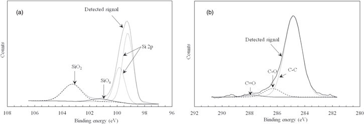
Fig. 3. Results of XPS analysis after baking nanodiamond-coated base wafer. (a) Si 2p spectra and (b) C 1 s spectra.
Download figure:
Standard image High-resolution image3.2. Observation and analysis of diamond layer deposited on base wafer
Figure 4 shows the OM observation results for the base wafer surface after depositing the diamond layer on the nanodiamond-coated base wafer. The thickness of the deposited diamond layer was 10 μm. Figure 4(a) shows a photograph of the 2 inch base wafer. Diamonds were deposited on the entire wafer. Figure 4(b) shows the OM observation. Diamonds were densely deposited, and the diamond grain size was under 10 μm. These grains were smaller than those of the diamond layer deposited by scratching using diamond powder.34)
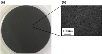
Fig. 4. Results of observing surface of 2 inch sample after depositing diamonds on nanodiamond-coated base wafer. (a) Photograph of 2 inch wafer and (b) OM observation.
Download figure:
Standard image High-resolution imageFigure 5 shows the results of XRD analysis for the deposited diamond layer. (111), (220), and (311) diffraction peaks were detected.35) The deposited diamond layer mainly consisted of (111) and (220) single crystals. We assume that polycrystalline diamond was deposited on the base wafer. In addition, Fig. 6 shows C1s photoemission spectra for the surface of the diamond layer deposited on the base wafer obtained by XPS analysis. The sp3 peak at 285.4 eV was mainly detected.36) Because native oxide was formed on the diamond layer, C–O bonding was also detected. Therefore, we concluded that the polycrystalline diamond layer was deposited on the base wafer using our proposed flow (Fig. 1).
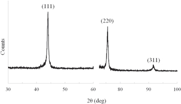
Fig. 5. Results of XRD analysis for diamond layer deposited on base wafer.
Download figure:
Standard image High-resolution image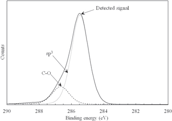
Fig. 6. C 1 s spectra for diamond layer deposited on base wafer obtained by XPS analysis.
Download figure:
Standard image High-resolution image3.3. Evaluation of roughness of polished diamond layer on base wafer
After the diamond layer was polished by CMP until its thickness was reduced from 10 to 8 μm, we evaluated the flatness of the polished surface using the AFM method. The average roughness (Ra) was 2–3 nm over 400 μm2. This value is sufficiently low to enable the bonding of another wafer and layer by SAB at room temperature in vacuum.37)
3.4. Evaluation and observation of voids formed when bonding silicon wafer to deposited diamond layer of base wafer by SAB
Figure 7 shows an IR transmission image of the above-mentioned sample after bonding a silicon wafer to the polished diamond layer by SAB at room temperature under a pressure of 1 × 10⁻⁵ Pa. There were no voids with gaps of over 200 nm in the wafer; this observation method can only detect gaps of over 200 nm. The silicon wafer was thus successfully bonded to the diamond layer by SAB.
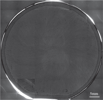
Fig. 7. IR transmission image of 2 inch wafer after bonding silicon wafer to diamond layer of base wafer.
Download figure:
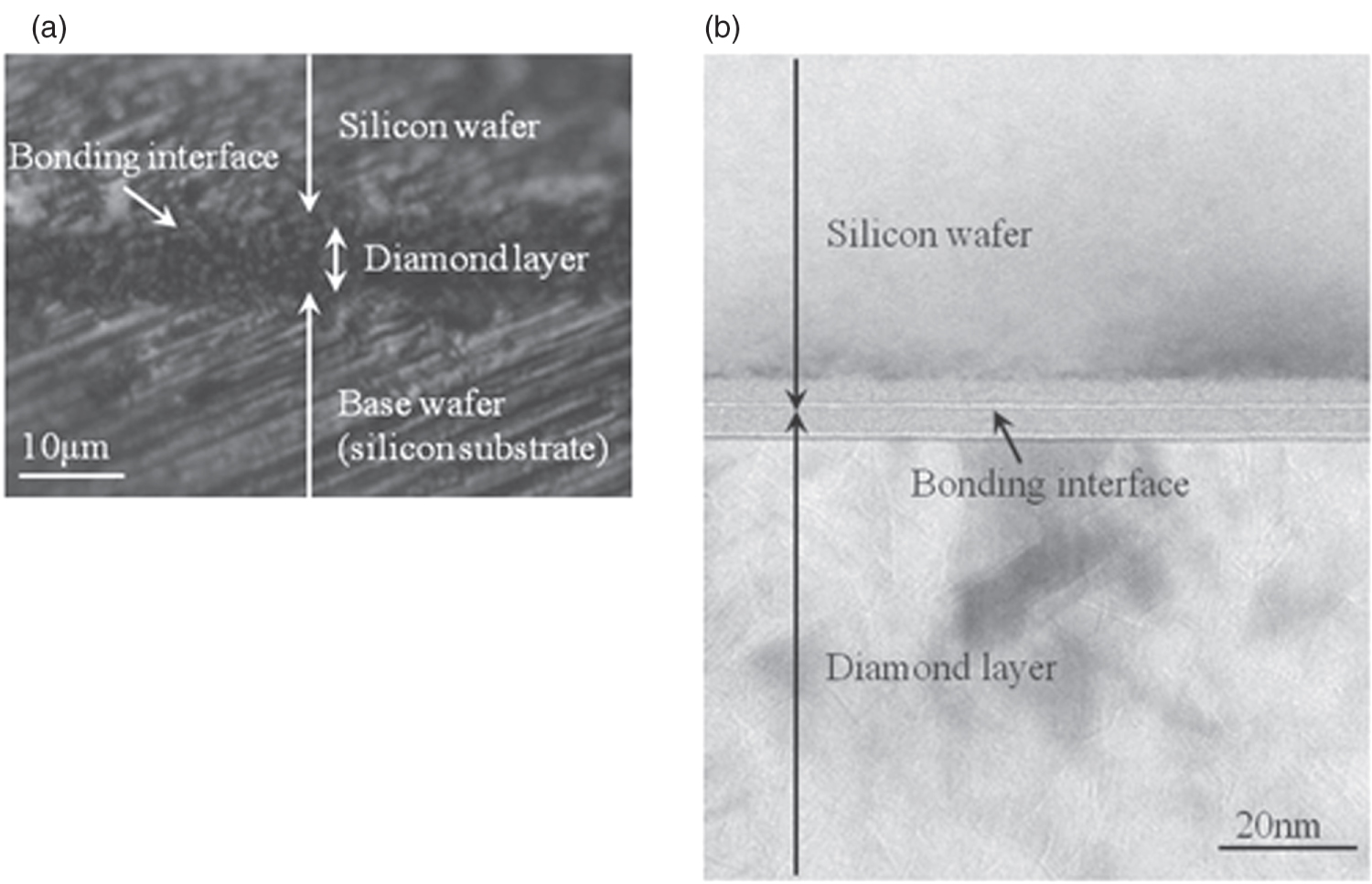
Standard image High-resolution imageWe also observed the bonded interface through cross-sectional OM and TEM micrographs of the chips obtained after dicing the bonded wafer at its center. Figures 8(a) and 8(b) show cross-sectional images obtained by OM observation and TEM observation, respectively. There were no voids with gaps of over 1 μm over a wide area, as shown in Fig. 8(a), and there were no voids with gaps of over 1 nm in the bonding region, as shown in Fig. 8(b). Therefore, we found that a silicon wafer can be bonded on a diamond layer of a base wafer without voids with gaps of over 200 nm.

Fig. 8. Cross-sectional observation images after bonding silicon wafer on diamond layer of base wafer. (a) Cross-sectional OM image and (b) cross-sectional TEM image.
Download figure:
Standard image High-resolution image3.5. Evaluation of depth profile of doping element in silicon layer on BOX layer
Because the devices were fabricated in a silicon layer on a BOX layer, it is important that the doping element concentration has a constant depth profile in the silicon layer. Thus, the depth profile of the concentration of phosphorus, an n-type conductor, was analyzed from the surface of the silicon layer to the bonding interface (the surface of the BOX layer) in the studied sample and reference sample (SOI wafer) by SIMS analysis.
Figure 9 shows the results of the SIMS analysis. The horizontal axis is the distance from the bonding interface and the vertical axis is the phosphorus concentration obtained from the SIMS analysis. For the studied sample [Fig. 9(a)], the concentration of phosphorus was constant from the top surface of the silicon layer to the bonding interface. However, for the reference sample [Fig. 9(b)], the concentration of phosphorus decreased from a depth of 0.2 μm to the bonding interface. We assume that phosphorus outdiffused from the silicon layer to the BOX layer in the reference sample during the bonding of the silicon wafer to the BOX layer at high temperatures of over 800 °C.
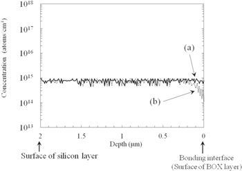
Fig. 9. Depth profiles of phosphorus concentration in silicon layer for studied and reference samples obtained by SIMS analysis after fabricating SOI wafer. (a) Studied sample, (b) reference sample.
Download figure:
Standard image High-resolution image3.6. Evaluation of depth profile of resistance in silicon layer on BOX layer
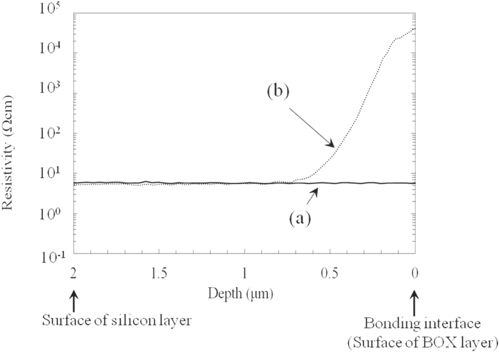
Because the devices were fabricated in a silicon layer on a BOX layer, it is also important that the resistivity has a constant depth profile in the silicon layer. The resistivity profiles of the studied sample and reference sample (SOI wafer) were investigated from the surface of the silicon layer to the bonding interface (the surface of the BOX layer) by SR measurement.
Figure 10 shows the results of the SR measurement. The horizontal axis is the distance from the bonding interface and the vertical axis is the resistivity obtained by SR measurement. For the studied sample [Fig. 10(a)], the resistivity was constant from the top surface of the silicon layer to the bonding interface.

Fig. 10. Depth profiles of resistivity in silicon layer for studied and reference samples obtained by SR measurement after fabricating SOI wafer. (a) Studied sample, (b) reference sample.
Download figure:
Standard image High-resolution imageHowever, for the reference sample (SOI wafer) [Fig. 10(b)], the resistivity increased from a depth of 0.8 μm to the bonding interface between the silicon layer and the BOX layer. At the interface, the resistivity was about 1 × 10⁴ times that in the region of constant resistivity between depths of 0.8 and 2.0 μm. This might have been due to the outdiffusion of the doping element (phosphorus) from the silicon layer to the BOX layer during thermal bonding at high temperatures of over 800 °C. According to Fig. 9(b), the concentration of phosphorus decreased by a factor of 10 from a depth of 0.2 μm to the bonding interface, thus increasing the resistivity by a factor of 10. Therefore, this increase in resistivity cannot be explained by the decreasing concentration of phosphorus. We consider that this increase in resistivity was caused by the formation of positive fixed charges38) in the BOX layer.
3.7. Evaluation of breakdown electric field of diamond-BOX layer
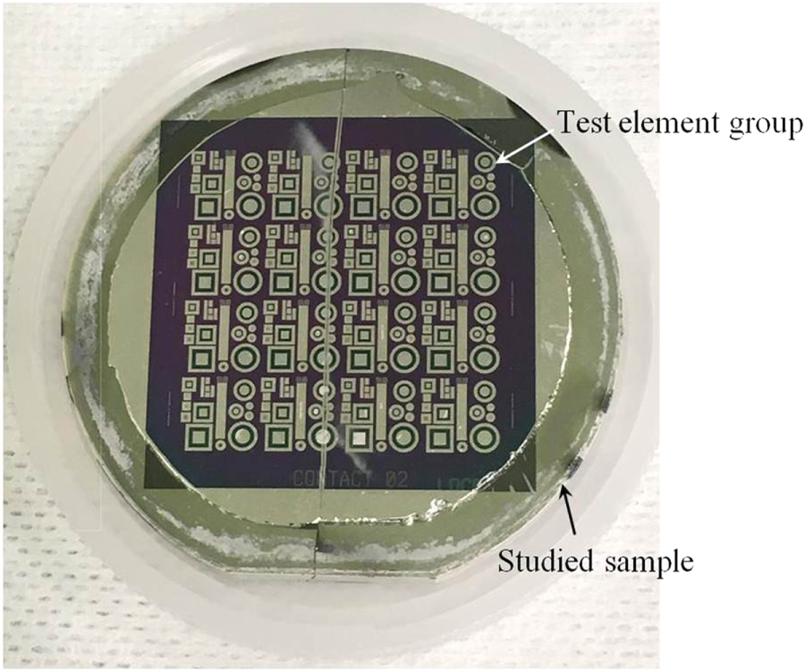
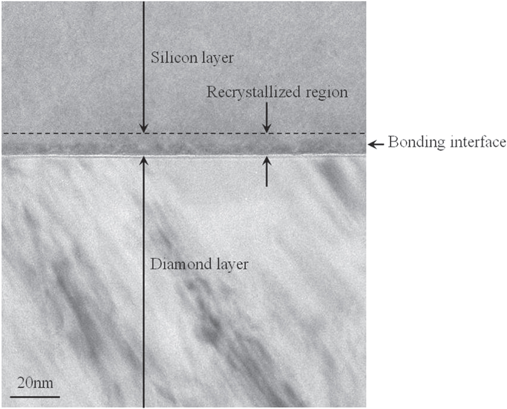
Figure 11 shows a photograph of the studied sample after devices were fabricated on it. Although the maximum temperature was 1000 °C, the silicon layer was not removed from the diamond layer during the fabrication of the devices. Figure 12 shows a cross-sectional TEM image of the studied sample after devices were fabricated on it. No gaps were generated at the bonding interface, and amorphous layers near the bonding interface were recrystallized after fabricating the devices. We found that the bonding strength obtained with the SAB technique was sufficient to fabricate the devices.

Fig. 11. (Color online) Photograph of studied sample after fabricating devices.
Download figure:
Standard image High-resolution image
Fig. 12. Cross-sectional TEM image of bonding interface after fabricating devices on studied sample.
Download figure:
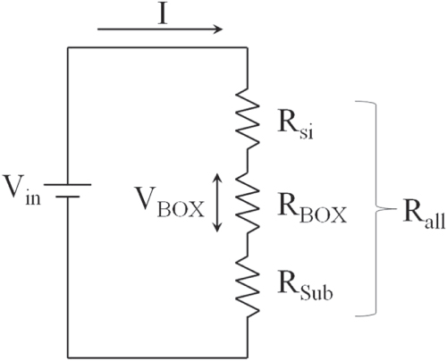
Standard image High-resolution imageWe measured the breakdown electric field of the BOX layer of the studied sample and the reference SOI sample using TZDB, which is a voltage-step-stress method. As a silicon substrate is supplied 0 V, the metal connected to the silicon layer has an additional input voltage of 0.1 V. Figure 13 shows the equivalent circuit schematic for the SOI wafer, where RSi is the resistance of the silicon layer, RBOX is that of the BOX layer, RSub is that of the base wafer, and Rall is the resistance from the top surface to the back side of the base wafer. Because RSi, RBOX, and RSub are connected serially,

As VBOX is the voltage applied to the BOX layer and Vin is the voltage input to the silicon layer, VBOX can be calculated using Ohm's law,39)

We can calculate RSi and RSub by multiplying the resistivity and thickness. It is necessary for calculating RBOX to measuring the resistivity of diamond layer. However, the contact resistivity between the probe of the measuring equipment and the diamond layer increased, using the four-terminal method and SR method. Thus, it is difficult to measure the resistivity of the diamond layer.
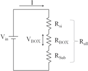
Fig. 13. Equivalent circuit schematic for SOI wafer.
Download figure:
Standard image High-resolution image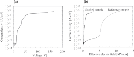
Fig. 14. TZDB measurement results for diamond-BOX layer. (a) Result for studied sample, (b) results for studied and reference sample.
Download figure:
Standard image High-resolution imageFrom Eq. (1),

Figure 14 shows the breakdown voltage and electric field for the studied sample and reference sample obtained by TZDB measurement. The measured area of the silicon layer was 1 mm2 as shown in Fig. 2(b). We calculated Rall from the I–V curve in Fig. 14(a). When the current density exceeds 2 × 10⁻¹⁰ A cm−2, we define Rall by the following equation in terms of the input voltage Vt and current It

Consequently, Rall is 4.6 × 10¹¹ Ω, RSi is 1.0 × 10⁻³ Ω, and RSub is 1.5 Ω.
When RBOX is much larger than RSi and RSub, RBOX satisfies

from Eq. (1). VBOX can be calculated from Eqs. (1), (2), and (5) as

In addition, we calculated the electric field by dividing VBOX by the thickness of the BOX layer, the results of which are shown in Fig. 14(b). The breakdown electric field was defined as the input voltage at which the leakage current reached 1 × 10⁻⁴ A cm−2. The breakdown electric field of the studied sample was 1 MV cm−1. Because the breakdown electric field of a polycrystalline diamond is about 1 MV cm−1,40,41) we consider that this result is reasonable. The breakdown electric field of the reference sample was 8.0 MV cm−1. Because the breakdown electric field of a thermal oxide is generally 8–15 MV cm−1,29) this result is also reasonable. We consider that the lower breakdown electric field of the studied sample than that of the reference sample was due to the grain boundaries in the polycrystalline diamond layer.42) We will attempt to study this issue in the future.
3.8. Evaluation of thermal conductivity of diamond-BOX layer
We evaluated the thermal conductivity of a base wafer with a diamond-BOX layer using a TCi thermal conductivity analyzer to transiently measure the resistivity at the surface of a sample after it was heated. We evaluated three samples: a silicon substrate as a reference sample, a SiO2 layer on a silicon substrate as another reference sample, and a diamond layer on a silicon substrate as the studied sample. The thickness of the base wafers and the silicon substrate was 500 μm and the thickness of the BOX layer was 4 μm.
Figure 15 shows the thermal conductivity of the three samples, which were 120 W mK−1 for the reference sample with the SiO2 layer, 348 W mK−1 for the studied sample with the diamond layer, and 291 W mK−1 for the silicon substrate without the BOX layer. The thermal conductivity of the studied sample was almost three times higher than that of the reference sample with the SiO2 layer and higher than that of the silicon substrate without a BOX layer.
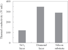
Fig. 15. Thermal conductivity of the three samples.
Download figure:
Standard image High-resolution imageAccording to the XPS analysis (Fig. 6), the studied polycrystalline diamond layer mainly has an sp3 structure and does not have an sp2 structure. Thus, the studied polycrystalline diamond layer has a similar thermal conductivity to the single-crystal diamond.
Because SiO2 has much lower thermal conductivity than silicon,43) and diamond has much larger thermal conductivity than silicon,44) we conclude that the results in Fig. 15 are reasonable. Therefore, the studied sample has high thermal conductivity and the diamond-BOX-SOI wafer will have similar thermal conductivity to a silicon substrate without a BOX layer.
3.9. Mechanism of seeding diamonds on base wafer
Diamond cannot be grown on a substrate of a different material without seeding elemental carbon. The seeding techniques are generally involve scratching the substrate using diamond powder13,15,16) and implanting carbon ions into the substrate by BEN.14) In this work, we did not use these seeding techniques to avoid damaging the surface of the base wafer. As an alternative, we spin-coated24) nanodiamond on the base wafer and baked the spin-coated base wafer.
According to the XPS results for the base wafer surface after baking the spin-coated base wafer shown in Fig. 3, we found that C–Si bonds do not exist on the base wafer, and the elemental carbon in nanodiamond does not connect directly to the elemental silicon in the base wafer. Then, we found that C–O and Si–O bonds existed on the surface of the base wafer after baking the spin-coated base wafer. Thus, we assumed that the elemental carbon on the surface of the base wafer bonded with the elemental silicon on the surface of the base wafer through the elemental oxygen, and we propose this seeding mechanism, that is thermal-treatment-wafer-bonding45–49) through the elemental oxygen after vaporizing H2O.
Figure 16 shows the mechanism of diamond seeding. In step (a), the nanodiamonds contained in water are spin-coated on a base wafer. Because water exists around each nanodiamond, the nanodiamond does not come in direct contact with the base wafer in this process. In step (b), the base wafer is baked at 80 °C. Only the wafer (H2O) coating the nanodiamonds is vaporized, and the carbon in the nanodiamonds is weakly bonded to the oxygen in the native oxide layer. In step (c), diamonds are deposited on the base wafer between 1000 °C and 1200 °C. In this process, the carbon is strongly bonded to the oxygen in the native oxide layer on the base wafer.
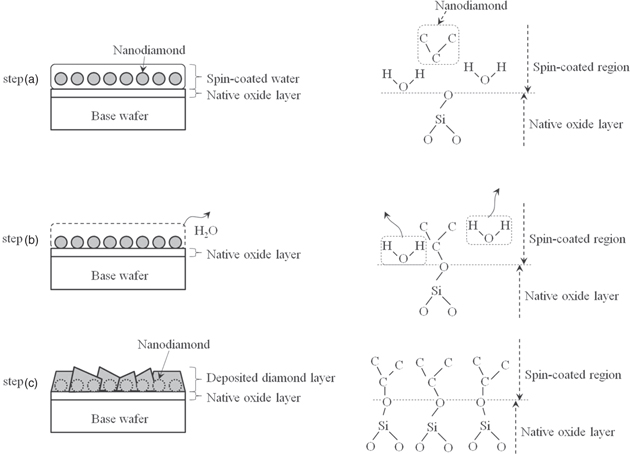
Fig. 16. Mechanism of diamond seeding on base wafer. Step (a): spin-coating nanodiamond wafer on base wafer, step (b): baking base wafer, and step (c): depositing diamond layer on base wafer.
Download figure:
Standard image High-resolution image3.10. Mechanism of SAB between polycrystalline diamond layer and bonding wafer
As shown in Fig. 8(b), according to the results of cross-sectional HR-TEM observation of the interface bonded by SAB, amorphous layers existed above and below the bonding interface. The thickness of these layers was about 5 nm. We found that these amorphous layers were formed by argon ion irradiation performed to induce SAB.50–53) This argon ion irradiation generated dangling bonds on the surface of the polycrystalline diamond layer and the bonding wafer at the same time. Figure 17 shows the mechanism of bonding between the polycrystalline diamond layer and bonding wafer for the studied sample (diamond-BOX-SOI wafer). In step (a), the surfaces of the bonding wafer and polycrystalline diamond layer are sputtered by argon ion irradiation in ultrahigh vacuum, and the dangling bonds are generated at these surfaces. Because these dangling bonds are stable in ultrahigh vacuum, the surfaces of the bonding wafer and polycrystalline diamond layer have dangling bonds, which can connect with other elements in ultrahigh vacuum. Thus, in step (b), when these bonds come close to each other, the dangling bonds at the elemental silicon in the bonding wafer become connected to the elemental carbon in the polycrystalline diamond layer.
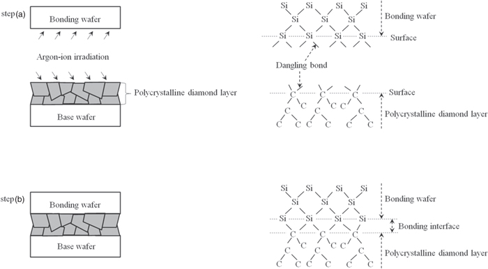
Fig. 17. Mechanism of bonding between diamond layer and bonding wafer by SAB. Step (a): Irradiation of argon ions to wafers, step (b): bonding of wafers.
Download figure:
Standard image High-resolution imageLiang and co-workers reported the bonding of a single-crystal silicon substrate to a single-crystal diamond substrate by SAB.53) They showed that the argon ion-irradiated region of the single-crystal diamond substrate had σ-connect-ions and π-connect-ions by electron energy loss spectroscopy (EELS), and that it had sp3 and sp2 bonds and no C–O bonds by XPS analysis. The σ-connect-ions and sp3 bonds showed that the single-crystal diamond was a cubic crystal system, and the π-connect-ions and sp2 bonds showed that the graphite had dangling bonds. The failure to detect C–O bonds indicated the removal of the native oxide layer on the diamond layer. Thus, the argon ion-irradiating could remove native oxide layer on diamond layer, maintained single-crystal diamond and could form dangling bonds on diamond layer. We clarified that the dangling bonds of the irradiated diamond substrate connected to those of the irradiated silicon substrate.
We also evaluated the crystal condition and bonding states in the bonding region of the polycrystalline diamond layer using EELS and XPS. Figure 18 shows the results of EELS analysis of the polycrystalline diamond layer and its bonding interface. Figure 18(a) shows the analyzed points. As shown in Fig. 18(b-1), a σ* peak was detected at 292 eV for the polycrystalline diamond layer, whereas a σ* peak was detected at 292 eV and a π* peak was detected at 286 eV near the bonding interface of the polycrystalline diamond layer, as shown in Fig. 18(b-2).
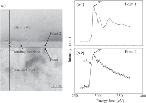
Fig. 18. Results of EELS analysis near bonding interface after fabricating SOI wafer. (a) Analysis points, (b-1) result of EELS analysis for point 1, and (b-2) result of EELS analysis for point 2.
Download figure:
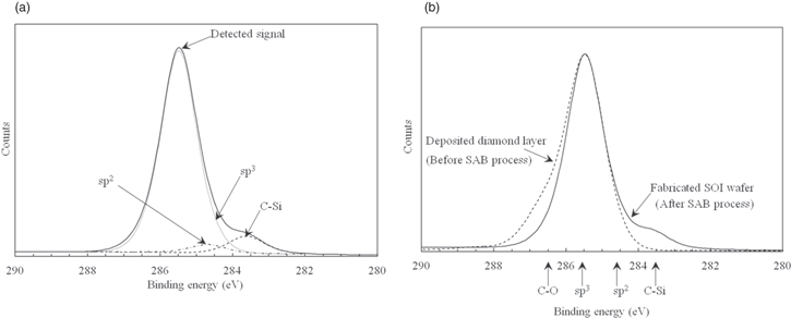
Standard image High-resolution imageTo evaluate how the silicon layer bonded to the polycrystalline diamond layer, only the silicon layer on the diamond layer of the studied sample was removed by CMP and etching. Then, we analyzed the top surface of the diamond layer after the SAB process by XPS. Figure 19 shows the results of the XPS analysis. According to the spectra in Fig. 19(a), sp3 bonds were mainly detected, although sp2 and C–Si bonds were also detected.32,36) Figure 19(b) shows additional spectra obtained after depositing a diamond layer on the base wafer (before the SAB process, Fig. 6). The surface of the diamond layer does not have sp2 or C–Si bonds after depositing the diamond layer but has sp3 and C–O bonds.
Fig. 19. C 1 s spectra of surface of diamond layer after fabricating SOI wafer obtained by XPS. (a) Result for fabricated SOI wafer, (b) results for deposited diamond layer (Fig. 6) and fabricated SOI wafer.
Download figure:
Standard image High-resolution image
These results are the same as those reported by Liang and co-workers.53) We clarified that the native oxide layer on the diamond layer was removed and that the sp2 structure was generated on the surface of the diamond layer by irradiating argon ions to the surface of the diamond layer. Moreover, C–Si bonds were generated by connecting the activated elemental silicon in the silicon wafer to the activated elemental carbon in the diamond layer. Therefore, we assume that our mechanism shown in Fig. 17 is reasonable.
4. Conclusions
We proposed a fabrication process for an SOI wafer with a diamond layer as a BOX layer that has high thermal conductivity. A diamond layer was deposited on a base wafer by spin-coating nanodiamonds and MW-CVD. The thermal conductivity of this deposited diamond layer was three times that of a SiO2 layer. Then, a silicon wafer was bonded to the diamond layer by SAB at room temperature in ultrahigh vacuum without forming any voids. This SOI wafer was used to fabricate devices making up a TEG at 1000 °C. Therefore, this diamond-BOX-SOI wafer has high thermal conductivity, and we consider that this SOI wafer will be useful for the fabrication of next-generation high-frequency and power devices.
Acknowledgments
The research was supported by Mr. Noritaka Ishigaki of Nihon Koshuha Co. Ltd., who assisted in the diamond deposition, Mr. Shogo Chiba of Saito Optical Science Ltd., who helped polish the diamond layer, Dr. Jun Utsumi and Mr Keiichiro Tsutsumi of Mitsubishi Heavy Industries Machine Tool Co. Ltd., who performed the bonding process, Mr. Shuzo Takeuchi of Fuzzy Logic Systems Institute, who gave advice on device fabrication, and Dr. Taisei Hirayama of Rigaku Co. for assistance in the evaluation of thermal radiation. The authors thank Dr. Hisashi Furuya and Mr. Naoki Ikeda of SUMCO for the management support and helpful discussions.