

Abstract
In this study, we report on ZnO-based flexible dye-sensitized solar cells (DSCs) doped with different concentrations of 5,10,15,20-tetraphenyl-21H,23H-porphyrin nickel(II) (NiTPP). The photoelectrodes were prepared by blade coating, followed by a hot-compression technique. The effects of NiTPP doping on the surface morphology, structural, optical, and photovoltaic properties were studied. The surface morphology was observed by scanning electron microscopy (SEM), which confirmed the presence of NiTPP particles and also some aggregated particles visible at higher doping concentrations. The structural properties were examined by X-ray diffraction analysis and Raman spectroscopy, which confirmed the hexagonal wurtzite ZnO structure. The crystallite size of the ZnO nanoparticles (NPs) increased while the lattice strain decreased with increasing NiTPP doping concentration. The increment in the crystallite size might have induced light scattering inside the film to some extent. Optical absorption spectra showed the broadening of the spectrum in the lower-wavelength region, and a new absorption peak appeared (at 422 nm) as an effect of NiTPP doping. The red and blue shifts were observed for that peak as an effect of various doping concentrations. The Raman study of the films showed that there is no significant changes in the ZnO or NiTPP crystallite structure because of the NiTPP doping at different concentrations. Photocurrent–voltage (I–V) analysis showed that the 0.7%-NiTPP-doped cell attained the highest light-to-electric conversion efficiency of 2.7% in this investigation, which was about 42% higher than that of a non-NiTPP-doped cell.
Export citation and abstract BibTeX RIS
1. Introduction
ZnO has been widely studied as an excellent photocatalyst and photoanode candidate for solar energy conversion applications,1–3) owing to its superior fundamental properties, including non-toxicity, low cost, and high electronic conductivity.4–9) It has a wide band gap energy (3.37 eV), a high exciton binding energy, a high electron mobility, a long carrier lifetime, a similar electronic band structure to TiO2, and excellent chemical stability, which have provoked intensive interest in terms of its dye-sensitized solar cell (DSC) application.10–14) Particle size and crystal morphology are important for this application, thus, the recent focus on the synthesis of nanocrystalline ZnO. There are several methods of preparing ZnO nanopartivles (NPs), such as sol–gel, precipitation, DC thermal plasma synthesis, spray pyrolysis, and hydrothermal synthesis.15,16)
Flexible and lightweight DSCs are receiving considerable interest owing to their potentials as renewable and mobile power sources for portable electronic devices.17–24) Conversion efficiencies of more than 5% have been reported for flexible ZnO-based DSCs25) although they are considerably lower than those of the cells prepared using glass substrates. In these cells, the sensitizer is considered a key component for harvesting solar radiation and converting it to electric current. The electrochemical, photophysical, and other properties of a sensitizer play a vital role in charge transfer dynamics at the semiconductor interface. Over the last 20 years, ruthenium complexes, which are used as a sensitizer, have maintained a clear lead in achieving an energy conversion efficiency of over 11%.26) DSCs based on nanoporous TiO2 electrodes on a glass substrate with the zinc porphyrin dye as the sensitizer have shown a conversion efficiency of over 12.5%.27) Because of the wide band gap nature of ZnO, it can only respond to ultraviolet (UV) light (4% in the solar spectrum). In order to capture photon energies in a broad range, different dyes are used as a sensitizer. Many metal complex dyes have been synthesized and used for DSC application. However, those dyes absorb only visible light in the wavelength range of 400–600 nm. Effective and controlled doping of a metal oxide photoanode with metal/nonmetal elements has been considered as a favorable method to modify the optoelectronic properties of wide-band-gap semiconductors.28–30) To increase photo-current density and power conversion efficiency, several investigations on doping of metal oxides have been carried out by enhancing the charge collection efficiency, charge transport, and suppressing recombination.31) In a conventional doping technique, the dopant is generally introduced during crystal growth via sol–gel or hydrothermal process.32,33) However, the doped impurities tend to form aggregates on the surface of host materials during the crystal formation stage, when the dopant concentration exceeds its solubility in the host crystal lattice.34) Moreover, the high-concentration doping sometime deforms the crystal lattice and ultimately the functional nanostructures of the host materials.35,36)
Synthetic porphyrins (and their corresponding metalloporphyrins) consist of a conjugated system of 22 π electrons, 18 of which are effectively delocalized to the Huckel requirement for aromaticity.37) Nickel tetraphenylporphyrin (NiTPP) has a similar structure to natural chromophores and is a suitable candidate as a light-harvesting material as it has structural stability and light absorption capability in the visible region. Porphyrins are generally photoexcited by a highly delocalized n-system, which has the capability to resist any major structural changes that can occur during oxidation.37) One of the most important advantages of using metelloporphyrin is its redox properties, which aid in generating porphyrin-excited states that can be favorable for photovoltaic cell applications. In this work, we adopted the well-known postgrowth doping strategy, in which we incorporated NiTPP at different percentages to prepare ZnO photoelectrodes. Porphyrin has a conjugated system consisting of 18 π electrons, which makes it a favorable candidate for organic semiconductor devices.38,39) The level of doping was optimized for the cells and characterized by scanning electron microscopy (SEM), solar simulator determination, X-ray diffraction (XRD) analysis, and UV–vis absorption spectroscopy.
2. Experimental procedure
2.1. Preparation of photoelectrodes
NiTPP and ZnO NPs were purchased from Aldrich and used without further purification. A schematic diagram of the molecular structure of NiTPP is shown in Fig. 1. NiTPP-doped ZnO photoanodes were prepared by the blade coating method. The blade coating paste was prepared using 0.35 g of ZnO NPs (<100 nm), 2 ml of ethanol (99.5%), and NiTPP at various percentages (0, 0.3, 0.7, 1, and 2) as a dopant material. The mixture was dispersed vigorously using a homogenizer (Sonic VCX-130) at 60% amplitude and  pulse rate for 30 min. Before coating, all the indium–tin-oxide coated poly(ethylene naphthalate) (ITO-PEN) substrates (∼15 Ω/square) were sequentially cleaned in an ultrasonic bath using acetone (twice) and methanol (once). The substrates were then dried in nitrogen gas flow and subsequently treated in a UV–ozone chamber (Filgen, Japan) for 20 min. The paste thus prepared was coated onto the substrates using polyimide tape as the frame and spacer. We coated the layer four times to obtain a thick, adherent layer photoanode. All the samples were air-dried at room temperature for 1 h. The target thickness of the film was in the range from 9 to 12 µm. After coating, the films were dried at 100 °C using a hot plate for 10 min and compressed using a mechanical compression machine (Mini TEST Press-10) at 130 MPa compression with 60 °C heating for 1 min.40)
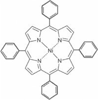
Fig. 1. Molecular structure of NiTPP.
Download figure:
Standard image High-resolution image2.2. Device fabrication
The prepared photoanodes were immersed in the 0.5 mM N719 dye (Solaronix Ruthenium-535 bis TBA) in ethanol solution. After 1 h, the photoelectrodes were removed from the dye solution. The photoelectrodes were then immersed two or three times in methanol solution with slight shaking to remove the extra loaded dye particles from the metal oxide NPs. After cleaning in methanol, all the samples were dried in nitrogen flow. Finally, DSCs were fabricated using a Pt-coated glass as a counter-electrode and by inserting a polymer film (Himilan, 50 µm) between the electrodes. The electrolyte (Solaronix Iodolyte AN 50) was inserted into the space between two electrodes through capillary action using a glass tube injector.
2.3. Characterization
The morphology of ZnO electrodes was observed by SEM (JEOL JSM-6510). The thickness of the ZnO film was examined using a profilometer (ULVAC Alpha-step 500). The current density–voltage (J/V) characteristics of the devices were determined under white light illumination at a standard solar irradiation of 100 mW/cm2 (AM 1.5) and in the dark using a JASCO CEP-25BX spectrophotometer J/V measurement setup with a xenon lamp as the light source and a computer-controlled voltage-current source meter (Keithley 238) at 25 °C. Structural characterization was performed using an XRD system (Rigaku RINT 2100 diffractometer) equipped with a Cu target, where a Ni-filtered Cu Kα radiation (λ = 1.5408 Å) was used. The X-ray tube voltage and current were 40 kV and 30 mA, respectively. The Raman shifts of the thin films were investigated using a Raman spectrometer (JASCO NRS-2100) at room temperature with Ar and Kr laser lines operating at 514.5 nm with a spectral resolution of 1 cm−1. Optical absorption was measured using a double beam spectrophotometer (JASCO 670 UV).
3. Results and discussion
3.1. Surface morphology
Figure 2 shows the surface morphologies of the ZnO photoanodes (a) without doping, (b) with 0.7% doping, and (c) with 2% doping. Figure 2(d) shows an enlarged view of NiTPP aggregates in a 2% NiTPP-doped sample, where the aggregates are visible on the photoanode surface. Without doping, the surface appears smooth and homogeneous. After 0.7% doping, the surface morphology did not change remarkably, and only some black dots are visible, which represent large NiTPP particles. By increasing the NiTPP doping concentrations to more than about 1%, the NiTPP particles are found to form many large aggregates of different sizes and shapes with ZnO NPs [Fig. 2(c)]. Figure 1(d) shows two such large aggregates of 15 and 25 µm sizes that were found in 2% doped photoelectrode.
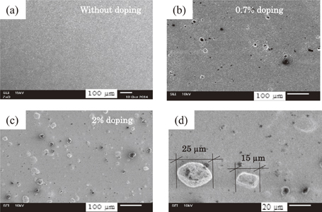
Fig. 2. SEM images of ZnO photoanode (a) without doping, (b) with 0.7% doping, (c) with 2% doping, and (d) enlarged view of NiTPP aggregates.
Download figure:
Standard image High-resolution image3.2. XRD
3.2.1. Crystallite structure of ZnO and NiTPP.
Figure 3 shows the XRD peaks of NiTPP powder (pink) and as-deposited ZnO films with NiTPP of various concentrations (0, 0.3, 0.7, 1, and 2%). No diffraction peaks for NiTPP were visible at low doping concentrations. However, the intensity of the (103) diffraction peak was improved considerably by increasing the NiTPP doping concentration. Also, some other diffraction peaks, such as (112), (004), and (323) appeared at high NiTPP doping concentrations. The diffraction peaks with different intensities indicate that NiTPP powder has a polycrystalline nature. The CRYSFIRE program41) was used to determine the parameters of a NiTPP unit cell and reported elsewhere.42) Structural data shows that the NiTPP powder has a tetragonal phase structure with the space group P43 characterized by (103)-preferred orientation. No extra diffraction peaks were found that corresponds to the Zn, Zn(OH)2, or ZnO phases, indicating that the ZnO NPs are pure and crystalline in nature. The sharp and narrow peaks indicate high quality, good crystallinity, and fine grain size. For the ZnO films, all the diffraction peaks correspond to the (100), (002), (101), (102), (110), and (103) planes and are perfectly indexed to the hexagonal wurtzite ZnO structure. These indicate that NiTPP doping does not change the crystal structure of ZnO. The absence of some NiTPP peaks in the XRD pattern that correspond to the (112) and (323) planes indicates some disorder or change in the NiTPP crystallite structure. The peak broadening changed for the ZnO diffraction peaks with increasing NiTPP concentration. This indicates the high crystallinity of the particles. A small right shift was observed for the positions of all the three diffraction peaks (100), (002), and (101) in the highly NiTPP-doped films. This small shift in the peak position can be attributed to the smaller ionic radii of Ni ions (0.083 nm for Ni2+, 0.070 nm for Ni+3, and 0.062 nm for Ni+4) than of Zn2+ ions (0.088 nm).43)
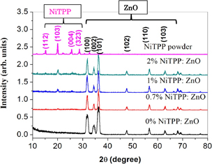
Fig. 3. XRD of NiTPP powder and NiTPP-doped ZnO photoanode at different concentrations.
Download figure:
Standard image High-resolution image3.2.2. Crystallite size estimation.
Various techniques are generally used for measuring particle size rather than crystallite size, such as direct light scattering (DLS), SEM, and transmission electron microscopy (TEM). Lattice strain is a measure of the distribution of lattice constants arising from crystal imperfections, such as lattice dislocations; it is investigated by X-ray line broadening.44) There are several methods of estimating crystallite size and lattice strain, such as the pseudo-boigt function, Rietveld refinement, Warren–Averbach analysis, Debye–Scherrer's formula, and Williamson–Hall (WH) analysis.45–50) In this work, we have used the Debye–Scherrer's formula and WH analysis to estimate the parameters. The mean crystallite size (D) of the NiTPP-doped ZnO films was estimated using the Scherrer formula51) (D = Kλ/β cos θ), where K is a constant whose value was considered as 0.9, λ is the wavelength of Cu Kα radiation considered to be 0.154 nm, and β is the full-width at half maximum (FWHM) of the diffraction peak. The crystallite sizes were estimated to be 8.2, 14.2, 14.9, 16.1, and 16.9 nm for the undoped and 0.3, 0.7, 1, and 2%-NiTPP-doped ZnO films, respectively (Table I). The data reveal that the presence of NiTPP in the ZnO matrix promotes the growth of crystal grains during mixing. Therefore, the ZnO crystallite order was improved by doping.
Table I. Structural parameters of NiTPP:ZnO NPs.
| NiTPP (%) | Scherrer method crystallite size (nm) | WH method | |
|---|---|---|---|
| Particle size (nm) | Strain (ε) (× 10) | ||
| 0 | 8.2 | 13.0 | 6.60 |
| 0.3 | 14.2 | 14.9 | 2.80 |
| 0.7 | 14.9 | 15.0 | 1.87 |
| 1 | 16.1 | 16.4 | 1.46 |
| 2 | 16.9 | 20.8 | 1.01 |
3.2.3. Estimation of lattice strain by WH analysis.
X-ray profile analysis is generally used to estimate the average particle size. Particle size and lattice strain are the two major quantities responsible for a change in peak broadening in an XRD curve. Lattice strain is a measure of the distribution of lattice constants that arises from the crystal imperfections, such as lattice dislocations. The WH analysis of the ZnO diffraction peaks was conducted to estimate the crystallite size and lattice strain. The strain induced in powder owing to crystal imperfections and distortions was calculated using.
where ε is the lattice strain, βhlk is the FWHM of the diffraction peak and is called the Bragg angle. Assuming that two terms (particle size and strain) contribute to peak broadening and are independent of each other, the observed peak breadth can hence be written as the sum of the particle size and strain as

By rearranging the above equation, we get

The above two equations [Eqs. (2) and (3)] are known as the WH equations. After fitting the data with a straight line to Eq. (3), crystallite size and the strain ε were calculated from the intercept and slope of the linear fit, respectively (Fig. 4). The calculated particle sizes from the WH plot are 13.0, 14.9, 15.0, 16.4, and 20.8 nm for the undoped and 0.3, 0.7, 1, and 2%-NiTPP-doped films, respectively (Table I). The crystallite size calculated by WH analysis is slightly higher than that calculated using the Scherrer formula. Hence, the resultant peak width is slightly smaller than that considered in the Scherrer formula. It is evident that the crystallite size increases and the lattice strain decreases with increasing NiTPP concentration. Grain boundaries, sinter stresses, stacking faults, and coherency stress are the possible sources of the developed strain in the ZnO host material.50) Also, the photoelectrode films were treated by hot-compression, which may generate few crystal disorders and in turn reduce the lattice strain.
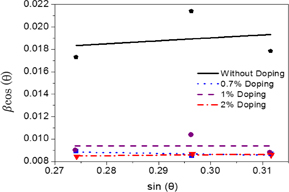
Fig. 4. Crystallite size/strain separation calculation using breadth according to WH method.
Download figure:
Standard image High-resolution image3.3. Raman study
We further investigated the crystal structure of NiTPP-doped ZnO photoelectrodes by analyzing Raman scattering spectra shown in Fig. 5. Two sharp Raman peaks at about 328 and 436 cm−1 are observed for the ZnO film. Between these, the peak at 436 cm−1 represents the  vibration mode52) of wurtzite ZnO and the 328 cm−1 peak represents the
  vibration mode.53) For the NiTPP-doped films,
  vibrational peak intensity is decreased by increasing the doping concentration. On the other hand, the
  peak intensity is increased for the high NiTPP doping concentrations. No significant Raman shift is observed in these vibrational modes as an effect of NiTPP doping concentration. Moreover, three less intense peaks for the ZnO NPs are observed at the 522, 675, and 780 cm−1 positions. The 522 cm−1 peak is left-shifted to the 499–503 cm−1 positions after NiTPP doping and the 675 cm−1 peak is right-shifted to 658–665 cm−1 positions. The peak intensity for both peaks (522 and 675 cm−1) are increased by NiTPP doping. The peak at position of 780 cm−1 is not visible for the NiTPP-doped films or the peak merged with the NiTPP peak at 756 cm−1 position. Both the NiTPP powder and NiTPP-doped ZnO NP films show some Raman vibration modes centered at the 399, 546, 638, 713, 739, 756, 799, 825, 848, 868, 887, and 901 cm−1 positions. Therefore, it confirms that NiTPP doping into the ZnO NP film does not change the NiTPP crystallite structure. Also, it does not change the ZnO crystallite structure but rather improves the crystallinity of the ZnO NPs to some extent.
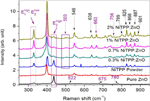
Fig. 5. Raman spectra of ZnO and NiTPP-doped ZnO photoelectrode films.
Download figure:
Standard image High-resolution image3.4. Optical properties
The effect of NiTPP doping into ZnO NPs on optical absorbance was investigated by UV-absorbance spectroscopy analysis in the range of 360 to 800 nm, as shown in Fig. 6. The inset shows the typical absorbance spectra of NiTPP. From the figure, it is clearly evident that, after the NiTPP doping, the absorbance increased for all the NiTPP-doped samples along with the emergence of a new peak at a wavelength of 422 nm, which is at the similar position found in the original NiTPP absorption spectra. In particular, the range of absorbance widened considerably in the lower-wavelength region (from 360 to 540 nm). The absorbance data are quite similar in pattern and amplitude at wavelengths of over 540 nm. However, absorbance increases with increasing doping concentrations up to 1% and then decreases for doping concentrations of more than 1%. The enhanced light absorbance of the porphyrin-doped cells probably corresponds to increased light-harvesting capabilities. NiTPP has π-conjugated electrons, which might exert several effects on the absorbance spectra including i) the increased absorbance in a particular wavelength range (in this investigation, high absorbance was found in the range of 360 to 540 nm), ii) the broadening of optical absorbance spectra, or iii) the shifting of peaks or the certain absorbance region toward longer wavelengths.37) In this investigation, we found that NiTPP doping only increases the absorbance within a certain range. Moreover, a slight bathochromic shifting of the 422 nm peak is observed as an effect of NiTPP doping. At low doping concentrations of upto 0.7%, we find a slight red shift in the absorbance spectra, whereas at doping concentrations of more than 1%, a blue shift is obtained (Fig. 6). Therefore, the red shift might reduce the energy gap of the film, while the blue shift might increase the energy gap.
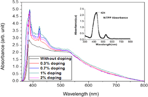
Fig. 6. UV-absorbance curve of photoelectrodes prepared using ZnO only and 0.3, 0.7, 1, and 2%-NiTPP-doped ZnO photoelectrodes.
Download figure:
Standard image High-resolution image3.5. Photovoltaic properties
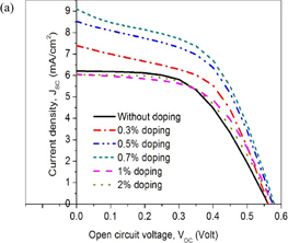
The photovoltaic performance of the cells as an effect of NiTPP doping is shown in Fig. 7. Figure 7(a) shows the photocurrent–voltage (I–V) plots, Fig. 7(b) the JSC and η plots, and Fig. 7(c) the open circuit voltage (VOC) and fill factor (FF) of the cells as a function of NiTPP doping concentration. From the figures, it is evident that the NiTPP doping concentration obviously affects the photovoltaic performance. Current density (JSC), and power conversion efficiency (η) increases up to 0.07% NiTPP doping and then decreases with further increase in the NiTPP doping concentration. Without NiTPP particles inside the cell, JSC and η are 6.2 mA·cm−2 and 1.86%, respectively. For the photoanodes doped with 0.3 and 0.7% NiTPP, the JSC and η of the cells were improved and reached 7.39 mA·cm−2 and 2.21%, and 9.2 mA·cm−2 and 2.68%, respectively. At 1 and 2% NiTPP doping concentrations, JSC decreased to 6.05 and 6.04 mA·cm−2 at η values of 1.94 and 1.87%, respectively.
Download figure:
Standard image High-resolution image
Download figure:
Standard image High-resolution image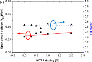
Fig. 7. (a) I–V curve of the cells prepared using NiTPP-doped ZnO photoelectrodes, (b) JSC and η as function of NiTPP doping concentration, and (c) VOC and FF as function of NiTPP doping concentration.
Download figure:
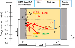
Standard image High-resolution imageThe reason for the improvement in η is mainly for the increment in JSC in NiTPP-doped cells; therefore, the cause of the increase in JSC is one of the vital concerns of this investigation. The JSC of a photovoltaic device is related to certain factors, such as the quality of films, changes in the charge transfer phenomenon, grain size, amount of dye loaded, internal resistance, mobility, and poor connectivity in the back contact region. Firstly, by considering the structural changes that occurred during cell preparation with NiTPP doping, we found that, at low doping concentrations, the surface morphologies did not change remarkably. The surface is smooth and homogenous, as we can see from the SEM image (Fig. 2). However, at high doping concentrations, many large aggregates were formed and also the adhesion of the film to the substrate was reduced. Therefore, it is reasonable to obtain better photovoltaic performance at low NiTPP doping concentrations. The XRD and Raman shift analysis reveals that NiTPP doping does not change the crystallite structure of the ZnO NPs. However, the crystallite size of the ZnO NPs increases, which was calculated using the Scherrer and WH equations. Therefore, NiTPP doping might induce the light scattering phenomenon to some extent inside the ZnO film, which may in turn contribute to a better excitation of electrons as well as to a high JSC. However, the improvement of the absorbance spectra does not stem from the light scattering phenomenon, because the absorbance is improved for a certain wavelength band. The improvement in JSC also indicates that the forward electron transfer from the photoexcited dye-NiTPP (donor) to the metal oxide (acceptor) is enhanced by the NiTPP doping of the cells. Figure 8 shows a schematic of the electron transfer process for the cells.54,55) This enhancement is due to the presence of electron facilitating groups in the molecular structure. In addition, the level of conjugation between the photosensitizer and metal oxide surface is important for an effective electron transfer process. A low NiTPP doping concentration allows for better physical conjugation, which is favorable for the effective electron transfer. The LUMO of NiTPP is slightly lower than that of N719 (Fig. 8), which is closer to the conduction band of the metal oxide. Thus, this can be the reason for the fast electron transfer at the dye-NiTPP/ZnO interface and a high current density. Moreover, the extra force induced during the electron transfer inside the film might also be the reason for the improvement of the charge separation process as well as for the decrease in the rate of charge recombination. Without NiTPP, electrons transfer from the dye to TiO2 at a lower force; therefore, there is a possibility of recombination for some electrons. However, at high NiTPP doping concentrations, the reduced electron transfer can be due to the structural defects generated owing to the formation of several larger aggregates. Therefore, these defects might decrease the interparticle connectivity and adhesion of the film to substrate. These aggregates might be the reason for the increased charge transport resistance at the ZnO-dye-electrolyte interface. Poor connectivity might increase the series resistance (RS) of the circuit and reduce JSC accordingly. Another phenomenon is the conversion of singlet excitons to triplet excitons because of the incorporation of NiTPP particles inside the films. As shown in the absorbance spectra, it is clear that the overall absorbance was increased along with a peak at 422 nm for the NiTPP-doped films. Thus, it is clear that the absorbance spectra was influenced by the NiTPP particles inside the ZnO film. Therefore, we can assume that, for the bare NiTPP films, a larger number of singlet excitons are generated by the absorption, whereas, in the case of NiTPP-doped cells, the change in the absorption spectra indicates that there may be a change in the type of generated excitons, which are mostly triplet excitons. The I–V results can be understood easily in terms of this concept. At high NiTPP doping concentrations, triplet excitons localize in the NiTPP phase islands, decreases JSC.56) The low overall power conversion efficiency at a high NiTPP doping concentration also indicates that the electron and hole carrier concentrations are unbalanced. Moreover, the red shift in the absorption curve at low NiTPP doping concentrations decreases the energy band gap, which also supports the concept of an extra driving force prior to charge separation. The VOC of the cells increases with increasing doping concentrations up to 0.7 and then decreased again with further increase in NiTPP doping concentration. This indicates a low shunt resistance (Rsh) at a high NiTPP doping concentration. Therefore, this confirms that the large aggregates cause a low Rsh with a low VOC. Figure 7(c) shows the VOC and FF plots as a function of NiTPP doping concentration. There is no significant change in the FF with varying NiTPP doping concentration. However, VOC increased slightly with increasing the NiTPP doping concentration. New peaks along with a red shift in the absorption spectra (Fig. 6) indicate the positive shift of a conduction band, which in turn might contribute to the increase in VOC. On the other hand, at high NiTPP doping concentrations, a blue shift causes a negative shift in the energy band, which might affect the low VOC.
Fig. 8. Energy diagram mechanism for a DSC based on the N719 sensitizer, iodolyte electrolyte, NiTPP-doped ZnO photoanode, and Pt cathode.
Download figure:
Standard image High-resolution image
4. Conclusions
We have introduced NiTPP as a successful dopant for ZnO-based flexible DSCs. Surface morphology images confirm the presence of NiTPP particles in the film. It also shows that a high NiTPP doping concentration creates a considerable number of microsized aggregates. Crystallite size increases and the lattice strain decreases for a NiTPP-doped film, calculated using the Scherrer and WH equations. Sharp peaks indicate that the crystallinity was not destroyed by incorporating NiTPP. Raman spectral analysis further confirms the wurtzite structure of the ZnO NPs in the film. After NiTPP doping, the presence of the vibrational modes at wavelengths of 327, 436, 503, 663, and 756 cm−1 confirms that NiTPP doping does not change the crystallite structure of the ZnO NPs. Moreover, the presence of NiTPP vibrational modes reveals that there is no significant change in the NiTPP crystallite structure. Optical absorption spectra show that NiTPP doping generates a new peak at a wavelength of 422, which indicates the presence of NiTPP particles inside the film. Also the bathochromic shifting of the 422 cm−1 absorption peak reveals that NiTPP doping concentration affects the energy gap. The red and blue shifts in the absorbance curve depending on the NiTPP concentrations are the reason for the variation in VOC of the cells. The increase in JSC has been clarified to be due to the improved forward electron transfer, reduced backward electron transfer, light scattering, and generation of triplet excitons for a NiTPP-doped cell. The photovoltaic performance data confirm that a low NiTPP doping concentration (0.7% is the optimum) is suitable for preparing an efficient flexible ZnO-based DSC.