
Abstract
An atomic layer etching process for silicon nitride (Si3N4) has been developed in which ammonium fluorosilicate [(NH4)2SiF6] is formed and desorbed using infrared annealing. The cycle of forming and removing ammonium fluorosilicate was repeated, demonstrating that the Si3N4 etching depth was accurately controlled with high selectivity to SiO2 by changing the number of cycle. An X-ray photoelectron spectroscopy peak, which had been previously assigned as N–H bond of an ammonium salt, was observed after radical exposure, indicating that the ammonium fluorosilicate-based modified layer had formed. This peak disappeared after infrared annealing for 10 s, demonstrating desorption of the modified layer. In thermal desorption spectroscopy, NH3, HF, and SiFx were detected, providing further evidence for the formation of the ammonium fluorosilicate-based modified layer. In addition, this layer has a multilayer structure, protecting the Si3N4 from exposure to reactive radicals.
Export citation and abstract BibTeX RIS

Content from this work may be used under the terms of the Creative Commons Attribution 4.0 license. Any further distribution of this work must maintain attribution to the author(s) and the title of the work, journal citation and DOI.
1. Introduction
Device structures are changing from planar-types to three-dimensional (3D) types, such as fin-type field-effect transistors (FinFET) and gate-all-around (GAA) transistors, in order to reduce leakage current and power consumption.1) Furthermore, fabricating these devices requires both high selectivity and precise control of device dimensions below the 10 nm scale.2)
Atomic layer etching (ALE), which involves the layer-by-layer removal of thin films, is expected to meet the requirements of both high selectivity and precise control of device dimensions.3–5) In the cyclic process of ALE, a reactive precursor is adsorbed on the surface to form a surface modified layer. Then this layer is removed. This cyclic process enables layer-by-layer removal of materials, which increases pattern fidelity and minimizes substrate damage. One essential characteristic of ALE is a self-limiting reaction because this characteristic enables the etching depth to be precisely controlled by changing the number of cycles. Although the etching depth in one cycle is not always a monolayer, we call such etching ALE if the etching process shows self-limiting behavior.
As atomic layer processing techniques, both atomic layer deposition (ALD) and ALE have been widely investigated. ALD, the counterpart of ALE, has been widely used in the semiconductor industry for depositing thin, conformal films.6,7) Although ALE has been studied since the 1990s, it is only beginning to be used in production because it has a longer process time and lower throughput than conventional etching. One key challenge to overcome in ALE is reducing the process time to provide sufficient productivity.
ALE methods have recently been reported for various anisotropic processes8–16) because current semiconductor manufacturing requires a critical dimension of less than 0.5 nm.4) For example, many studies have demonstrated the ALE of Si based on Cl2/Ar chemistry because the monolayer adsorption of Cl atoms on a Si surface followed by Ar+ ion bombardment is expected to achieve layer-by-layer self-limiting etching.8–11) In addition to Si, ALE processes of SiO2 and Si3N4 have been developed in which a fluorocarbon passivation layer is formed on etched surfaces followed by etching with Ar+ ion bombardment with incident energies of up to 50 eV.12–16)
To fabricate 3D devices, such as FinFET and GAA transistors, isotropic ALE will be required to isotropically remove thin films with atomic level precision. Isotropic ALE based on spontaneous thermal chemistry has recently been reported for metal oxides and silicon oxides. ALE processes of Al2O3 and HfO2 using sequential, self-limiting thermal reactions with tin(II) acetylacetonate [Sn(acac)2] and hydrogen fluoride (HF) as the reactants17–19) have been reported. As first reported by Nishino et al. in 1993,20) ammonium fluorosilicate is formed and sublimated in the ALE of SiO2. In the etching procedure, an ammonium fluorosilicate film is formed on the SiO2 surface after being exposed to reactive gas molecules or radicals in plasmas.21–25) Then, the etched surface is thermally annealed above 100 °C to sublimate the film of ammonium fluorosilicate. These isotropic ALE processes are also called thermal ALE because of the thermal reactions to form and remove surface modified layers.
Silicon nitride (Si3N4) must be selectively etched over Si or SiO2 to fabricate next-generation 3D devices.26–28) One important challenge in developing isotropic Si3N4 ALE is to form a surface modified layer on a Si3N4 surface. Knolle and Huttermann reported that CF4/O2 plasmas produce an ammonium fluorosilicate-based modified layer on a Si3N4 surface.29) In addition, they found that this modified layer acts as an etching stop layer of Si3N4. Several studies subsequently reported that an (NH4)2SiF6 layer formed on a Si3N4 surface after it had been exposed to plasmas using hydrofluorocarbon30) and NH3/NF3/O231) gas mixtures.
An isotropic and selective ALE process has recently been developed to precisely remove Si3N4 films.32) In this process, a Si3N4 surface is exposed to hydrofluorocarbon-based plasma to form an ammonium fluorosilicate-based modified layer. Then, the substrate is thermally annealed to sublimate the modified layer. The modified layer is repeatedly formed and sublimated in this way to obtain the required etching depth.
One key challenge in using ALE in mass production is to reduce the process time to obtain a high-throughput. In our previous report,32) the modified layer was desorbed by heating the sample stage with the circulation of a fluid, resulting in a long desorption step time. Therefore, the desorption step time must be reduced to use ALE in mass production.
In this study, surface modified layers were formed and desorbed using infrared (IR) annealing to develop high-throughput ALE of Si3N4. Surface modified layers were rapidly desorbed by using IR annealing. A cycle of radical exposure and IR annealing was repeated, demonstrating that the ALE process of Si3N4 is self-limiting and highly selective with respective to SiO2. Since previous studies focused on the surface analysis of the modified layer using X-ray photoelectron spectroscopy (XPS) and Fourier transform infrared spectroscopy (FTIR),29,30,32) no experimental studies have addressed the desorption of the modified layer, to the best of our knowledge. Thermal desorption spectroscopy (TDS) was conducted to clarify the desorption species from the modified layer and to investigate its structure.
2. Experimental methods
A schematic diagram of one cycle of the ALE in this study is shown in Fig. 1. In the first step of this process, the Si3N4 surface is exposed to radicals generated by a hydrofluorocarbon-based plasma. A surface modified layer of ammonium fluorosilicate is formed by the reaction between Si3N4 and incident radicals. In the second step, the substrate is thermally annealed at a temperature above the decomposition of ammonium fluorosilicate. Then, the reaction products desorb from the surface, which results in the removal of the modified layer. The ammonium fluorosilicate-based modified layer is repeatedly formed and desorbed this way until the etching depth reaches a target value.
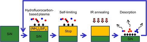
Fig. 1. Schematic representation of isotropic ALE of Si3N4 by forming and removing surface modified layer. While the modified layer is forming, the Si3N4 surface is exposed to radicals generated in a hydrofluorocarbon-based plasma. IR annealing enables the modified layer to be rapidly desorbed.
Download figure:
Standard image High-resolution imageFigure 2 shows a schematic diagram of the experimental apparatus used in this study. The apparatus consists of a plasma source that produces radicals and a reaction chamber. Blanket samples of Si3N4 and SiO2 were placed in the reaction chamber. By connecting a turbomolecular pump to the reaction chamber, a gas flow transported radicals from the plasma source to the reaction chamber. The samples of Si3N4 and SiO2 were set 500 mm from the plasma so that they were exposed to only radicals without ions.
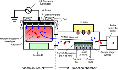
Fig. 2. Schematic diagram of remote-type etching apparatus consisting of plasma source and reaction chamber. Radicals generated in the plasma source are transported to the reaction chamber through a gas flow. The plasma is 500 mm from the sample.
Download figure:
Standard image High-resolution imageA source RF power of 200 MHz to generate plasma was supplied to a top antenna plate. Solenoid coils were set to control the plasma distribution. The samples used in this study were low-pressure chemical vapor deposition (LP-CVD) Si3N4 and thermally grown SiO2. Samples were held on the sample stage with a mechanical chuck. Helium gas was confined between the sample and the stage to improve thermal conductivity. The pressure of the helium gas was 1.5 kPa. Since the thermal decomposition temperature of (NH4)2SiF6 is approximately 130 °C, the sample was kept at 20 °C during the radical exposure to form the modified layer. An IR annealing lamp (Ushio UL-SH-01) was mounted above the sample stage. The irradiated energy density of IR annealing was 10–20 W/cm2. Hydrofluorocarbon-based chemistry was used in this experiment.32) The RF power supplied to the plasma source was 400 W.
The modified layer on the Si3N4 surface was analyzed using XPS (Thermo Fisher Scientific Theta Probe). The XPS analysis, with a spatial resolution of 400 µm, was performed at a take off angle of 36° with respect to the surface using a monochromated Al Kα X-ray source. The etching depth of Si3N4 and SiO2 samples was measured using a spectroscopic reflectometer (Nanometrics NanoSpec 5100).
The desorption process of the modified layer was investigated using TDS. After the sample was exposed to radicals generated by the hydrofluorocarbon-based plasma, it was transferred ex-situ to the TDS analysis chamber (ESCO EMD-WA1000S/W). The sample was heated from room temperature to 500 °C at a constant rate of 0.5 °C/s. The desorption of species with a mass-to-charge ratio (m/z) from 1 to 200 was monitored using a quadrupole mass spectrometer. The ionization energy in the spectrometer was 70 eV.
3. Results and discussion
3.1. Cyclic etching of Si3N4 using a self-limiting process
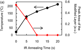
One essential characteristic of ALE is a self-limiting reaction because this characteristic enables etching the depth to be precisely controlled by changing the number of cycles. Here, we measured the etching depth of Si3N4 after exposure to hydrofluorocarbon-based plasma and IR annealing. The surface temperature during radical exposure was kept at 20 °C. The temperature of the Si3N4 sample during IR annealing was increased up to 150 °C within 10 s [see Fig. 6(a)]. The etching depth as a function of the radical exposure time is shown in Fig. 3. The etching depth increased and saturated at about 1.2 nm as the radical exposure time was increased to over 300 s. Therefore, a self-limiting etching process for Si3N4 was obtained after radical exposure and IR annealing.
Download figure:
Standard image High-resolution image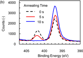
Fig. 6. (a) Temperature of Si3N4 sample and XPS peak area of modified layer during IR annealing. (b) XPS intensity of N 1s spectra obtained after IR annealing. The area of the XPS peak the modified layer is calculated from the peak at the binding energy of 402 eV.
Download figure:
Standard image High-resolution image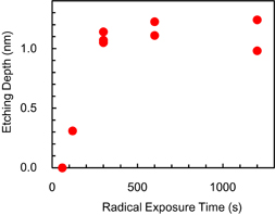
Fig. 3. Etching depth of Si3N4 as a function of the radical exposure time. The etching depth was measured after a modified layer was formed and removed. After the modified layer was formed, the Si3N4 sample was annealed up to 150 °C.
Download figure:
Standard image High-resolution imageNext, the cyclic etching of Si3N4 was investigated by repeating the cycle of radical exposure and IR annealing. The radical exposure time was 300 s, and the Si3N4 sample was annealed up to 150 °C. After IR annealing, the sample was cooled to the stage temperature of 20 °C by supplying He gas from behind the sample and the next cycle was started. The number of cycles was varied between 1 and 10. The etching depth as a function of the number of cycles is shown in Fig. 4. The etching depth of SiO2 is also shown here to evaluate the selectivity of the etching. The etching depth of Si3N4 increases linearly as the number of cycles increases. The etching rate is 1.6 nm/cycle, enabling us to control the etching depth with nanometer level accuracy. In contrast, the etching depth of SiO2 is under the detection limit of our measurement system. These results demonstrate that the etching process of Si3N4 that forms and removes the modified layer is highly selective with respect to SiO2. Two reasons may be considered for the high selectivity to SiO2: (1) As described in the next section, we confirmed that an ammonium fluorosilicate-based modified layer was formed after exposure to hydrofluorocarbon-based plasma. This layer does not form on the surface of SiO2 because no nitrogen atoms are included in the gas phase during radical exposure using the plasma. (2) The contribution of reactive ion etching is negligibly small. The etching apparatus used in this study is a remote plasma type with a radical exposure distance of about 500 mm, reducing the ion current flux on the sample to less than 1 × 10⁻⁵ mA/cm2.
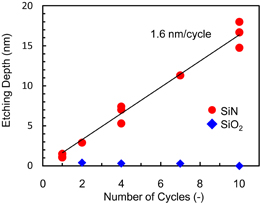
Fig. 4. Dependence of etching depth of Si3N4 on number of cycles. The solid line was obtained using the least square method. The radical exposure time was 300 s. The sample was annealed up to 150 °C and cooled to 20 °C in each cycle.
Download figure:
Standard image High-resolution image3.2. Formation process of the ammonium fluorosilicate-based modified layer
Surface analysis using XPS was conducted to clarify the chemical composition of the modified layer that formed on the Si3N4 surface after exposure to the hydrofluorocarbon-based plasma. The N 1s spectrum obtained after radical exposure is shown in Fig. 5. The spectrum of Si3N4 before radical exposure is also shown for comparison. The radical exposure time to form the modified layer was 1200 s. The peak at the binding energy of 397 eV originates from bulk Si3N4. A peak at the binding energy of 402 eV, attributed to the ammonium salt, was observed while the XPS intensity at 397 eV decreased after radical exposure. Wang and Luo identified a N 1s peak at around 401 eV, observed on Si3N4 etched in NF3/O2/NH3 plasmas, as an NH4+ salt using XPS.31) An ammonium fluorosilicate-based modified layer on Si3N4 was first observed by Knolle and Huttemann.29) They reported that ammonium fluorosilicate [(NH4)2SiF6] forms on Si3N4 during CF4 plasma etching when the surface of Si3N4 is hydrogenated and oxidized. From these previous studies, the peak at 402 eV in this study indicates that the ammonium fluorosilicate-based modified layer was formed after exposure to the hydrofluorocarbon-based plasma.
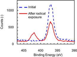
Fig. 5. XPS intensity of N 1s spectrum obtained after radical exposure (red solid line). The N 1s spectrum before radical exposure (blue dotted line) is also shown for comparison. The radical exposure time was 1200 s. The peaks at 397 and 402 eV are respectively assigned to bulk Si3N4 and the ammonium fluorosilicate-based modified layer.
Download figure:
Standard image High-resolution image3.3. Desorption process of the modified layer
The desorption process of the ammonium fluorosilicate-based modified layer was investigated to demonstrate desorption using IR annealing for high-throughput ALE. After exposure to hydrofluorocarbon-based plasma, the sample of Si3N4 was annealed using an IR lamp and transferred ex-situ to the XPS analysis chamber. The radical exposure time was 300 s because the formation of the modified layer saturated after 300 s (as shown in Fig. 3). The irradiated energy density of IR annealing was kept at 20 W/cm2. The temperature of the Si3N4 sample as a function of the IR annealing time is shown in Fig. 6(a). During IR annealing, the temperature of the sample exceeded 120 °C, which is the thermal decomposition temperature of (NH4)2SiF6, within 10 s. Figure 6(b) shows N 1s spectra obtained after the IR annealing. The annealing time was varied from 5 to 10 s. The spectrum before IR annealing, the annealing time of which is 0 s, is also shown for comparison. The peak at the binding energy of 402 eV, which is assigned to the modified layer, disappeared as the annealing time increased, while the peak of bulk Si3N4 at the binding energy of 397 eV increased. The time dependence of the area of the XPS peak of the modified layer is also shown in Fig. 6(a) (right axis). The area of the peak monotonically decreased as the annealing time increased, and the modified layer was completely removed within 10 s.
In the TDS analysis, thermal desorption (TD) spectra were obtained to clarify the desorption species from the modified layer. In this analysis, the Si3N4 samples after radical exposure were transferred ex-situ to the TDS chamber. The TD spectra during annealing from 100 to 300 °C are shown in Fig. 7. Desorption species with a m/z of 15, 16, and 17 were observed during annealing from 130 to 230 °C, originating from NH3. To estimate the desorption flux of NH3+ (m/z = 17), the flux of OH+ (m/z = 17), which can be estimated from the flux of H2O (m/z = 18) assuming that the fragment ratio is 0.26, was subtracted from the total flux with m/z = 17. HF (m/z = 19) and SiFx (x = 1–4, m/z = 47, 66, 85, 104) molecules were also detected as desorption species during the annealing from 130 to 230 °C. These results revealed that NH3, HF, and SiFx (x = 1–4) are the desorption species from the modified layer during the annealing up to 200 °C. Previous work using XPS revealed that the compositional ratio of  in the modified layer is roughly
  .32) The desorption of NH3 and HF shows that the modified layer included hydrogen atoms, which can not be detected by XPS. The desorption species in combination with the compositional ratio obtained from the XPS analysis32) provides supporting evidence for the formation of the ammonium fluorosilicate-based modified layer on the Si3N4 surface. Assuming that the chemical composition of the modified layer is (NH4)2SiF6 and that silicon atoms desorb as SiF4, the thermal decomposition reaction can be written as

However, note that the silicon to nitrogen (Si to N) ratio according to Eq. (1) is  , which is smaller than that of bulk Si3N4 of
  . The XPS analysis of the Si3N4 surface after the desorption of the modified layer shows that the Si to N ratio is similar to the initial (before radical exposure) value of
  . Therefore, several mechanisms can explain why a larger number of Si atoms than that according to Eq. (1) are removed:
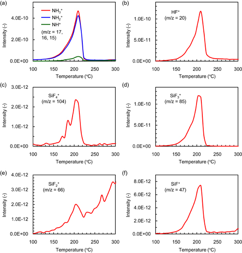
Fig. 7. Thermal desorption spectra obtained from modified layer on Si3N4 sample after exposure to hydrofluorocarbon-based plasma. The flux of OH+ (m/z = 17) was subtracted from the total flux with m/z = 17.
Download figure:
Standard image High-resolution image- (1)Si atoms are removed as SiFx molecules during radical exposure.
- (2)The ratio of Si to N in the modified layer is larger than
 according to Eq. (1).

Next, we focus on the desorption kinetics during the annealing to investigate the structure of the modified layer. The TD spectra in Fig. 7 show an exponentially increasing leading edge (from 130 to 200 °C) and a high-temperature cutoff at 210 °C. These are the characteristics of zero-order desorption kinetics,33) suggesting that the modified layer has a multilayer structure. To provide a theoretical justification for zero-order desorption, the TD spectra were analyzed by using Arrhenius plots. At a constant rate of temperature increase during annealing (0.5 °C in this study), the intensity of the TD spectrum is proportional to the rate of desorption Rdes, which is commonly described by the following Arrhenius equation:33)

where ν is the pre-exponential frequency factor, θ the adsorbate coverage, n the order of desorption, Edes the activation energy for desorption, and T is the surface temperature. Figure 8 shows Arrhenius plots for Rdes of NH3, HF, and SiF3 taken from the leading edge of Rdes shown in Fig. 7. The data are well fitted with straight lines, indicating that the order of desorption n is 0 and the modified layer has a multilayer structure. This multilayer structure protects the Si3N4 surface from exposure to reactive radicals, which might lead to the self-limiting formation of the modified layer.
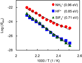
Fig. 8. Arrhenius plots for rates of desorption Rdes of NH3, HF, and SiF3. Values in parentheses are activation energies for the desorption.
Download figure:
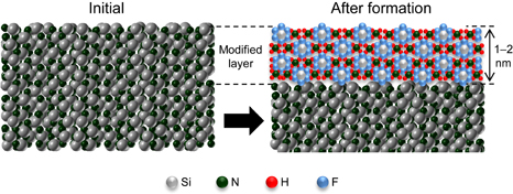
Standard image High-resolution imageHere, we discuss the self-limiting formation of the modified layer. The saturation of the etching depth in Fig. 3 indicates the saturation of the thickness of the modified layer during radical exposure. We assumed that the formation process of the modified layer on Si3N4 is similar to that of surface oxidation on Si and metals.34,35) The modified layer on Si3N4 is schematically illustrated in Fig. 9. Reactive radicals adsorb on and react with the surface of Si3N4. At the surface temperature of 20 °C, the reaction products form the ammonium fluorosilicate-based modified layer because its thermal decomposition temperature is over 100 °C. As described above, the modified layer has a multilayer structure. After reaching a thickness of several layers, the modified layer protects the surface of Si3N4 from exposure to the reactive radicals, which might lead to the self-limiting formation process. Knolle and Huttermann reported that the thickness of an ammonium fluorosilicate layer that is converted from Si3N4 is equal to the etching depth of Si3N4 after forming and removing this layer.29) While the etching depth of SiO221) after forming and removing ammonium fluorosilicate depends on the so-called parabolic relationship in the classical Deal–Grove model,36) where the etching depth increases with the square root of the radical exposure time, the etching depth of Si3N4 shown in Fig. 3 does not follow this relationship. As a future work, the mechanism of the self-limiting formation will be investigated by classical molecular dynamics simulation.
Fig. 9. Schematic illustration of ammonium fluorosilicate-based modified layer on Si3N4 surface. The modified layer has a 1–2-nm-thick multilayer structure.
Download figure:
Standard image High-resolution image
The activation energy for desorption Edes can be obtained from the slope of the Arrhenius plots in Fig. 8. The activation energies Edes are 0.96, 0.85, and 0.71 for NH3, HF, and SiF3, respectively. The activation energy Edes includes contributions from both the activation energy for the thermal decomposition reaction [Eq. (1)] and the interaction energy between the desorption species and the surface. The difference in the value of Edes for NH3, HF, and SiF3 is attributed to the latter component.
4. Conclusions
The high-throughput and selective atomic layer etching (ALE) of silicon nitride (Si3N4) has been developed by forming and removing a surface modified layer. Infrared (IR) annealing was used to rapidly desorb modified layers. Etching depth measurement, X-ray photoelectron spectroscopy (XPS), and thermal desorption spectroscopy (TDS) were used to examine Si3N4 ALE.
The cyclic etching of Si3N4 was investigated by repeatedly forming and removing the ammonium fluorosilicate-based modified layer. The etching depth of Si3N4 increased linearly as the number of cycles increased with an etching rate of 1.6 nm/cycle while no etching of SiO2 was observed. These results demonstrate that the Si3N4 etching depth can be accurately controlled with high selectivity to SiO2 by changing the number of cycles, which is promising for next-generation 3D device fabrication.
Surface analysis using XPS after radical exposure to hydrofluorocarbon-based plasma revealed a N 1s peak at the binding energy of 402 eV. This peak had been previously assigned as the N–H bond of an ammonium salt, indicating that the ammonium fluorosilicate-based modified layer was formed on the Si3N4 surface. This XPS peak disappeared after IR annealing for 10 s. This result shows that IR annealing rapidly removes the modified layer to achieve high-throughput ALE.
The TDS was conducted to clarify the desorption species from the modified layer and to investigate its structure. In this analysis, NH3, HF, and SiFx (x = 1–4) were detected as desorption species from the modified layer at an annealing temperature from 130 to 200 °C, providing further evidence for the formation of the ammonium fluorosilicate-based modified layer. The desorption processes of these molecules follow zero-order desorption kinetics, indicating that the modified layer has a multilayer structure. This multilayer protects the Si3N4 surface from exposure to reactive radicals, which might result in the self-limiting formation of the modified layer.