Abstract
This paper reports the mechanical and electrical characteristics of Ge/Ge interfaces prepared by room-temperature surface-activated bonding (SAB). Bonded Ge/Ge wafer pairs with high bonding strength equivalent to that of the bulk material were achieved without any heat treatment. It was found that the bonding of Ge wafers was not sensitive to the background vacuum pressure in a wafer-bonding chamber compared with the bonding of Si wafers. The current–voltage characteristics and microstructures of bonded interfaces formed by SAB and low-temperature plasma activation bonding (PAB) were compared. It was demonstrated that junctions with very low resistivity can be obtained by SAB at room temperature.
Export citation and abstract BibTeX RIS
1. Introduction
Germanium (Ge) is an attractive material for advanced far-infrared (FIR) photon detectors. In particular, a Ge blocked impurity band (BIB) detector1–7) is expected to provide an extended long-wavelength response (λ > 200 µm) with low dark current. A Ge BIB device is composed of two layers, a pure blocking layer, and a heavily doped absorbing layer, which serves as the active layer of the device. Epitaxial growth techniques have been used to form the two-layer structure. However, the typical high-temperature growth process using chemical vapor deposition and liquid-phase epitaxy resulted in dopant diffusion into the pure substrate during the high-temperature growth process (>650 °C).5,8)
Direct wafer bonding is a promising alternative approach to epitaxial growth. Many wafer bonding methods such as oxygen plasma activation bonding (PAB) have been studied to create novel device structures for a wide range of applications.9–12) However, conventional PAB methods need an annealing process to increase the bonding strength, which often leads to void generation. Surface-activated bonding (SAB) is a room-temperature bonding method.13,14) It has been reported that the SAB of Si in ultrahigh vacuum (UHV) allows void-free interfaces to be achieved even after postbonding annealing.15) Recently, the SAB of Ge wafers has also been reported for infrared detectors.16–21) However, little work has focused on the effects of the bonding conditions on the mechanical and electrical properties and microstructure of the Ge/Ge bonded interface.
In this study, we demonstrate the room-temperature bonding of Ge wafers using SAB. We evaluate the bonding strength through razor blade, tensile, and dicing tests and examine the interface state through current–voltage (I–V) measurements and transmission electron microscopy (TEM) observations. For the I–V measurements and TEM observations, directly bonded Ge/Ge interfaces are prepared by SAB and PAB for comparison.
2. Experimental procedure
Commercially available 2-in. Ga-doped p-type, epi-ready, (100)-oriented Ge wafers were used in wafer bonding. The thickness of the wafers was 500 ± 25 µm. Since the surface roughness has a strong effect on direct wafer bonding, the surface roughness of the Ge wafers was measured using an atomic force microscope (AFM).
In order to evaluate the native oxide and hydrocarbon contamination of the as-received Ge wafers, X-ray photoelectron spectroscopy (XPS) measurements were carried out. Using argon fast atom beam (Ar-FAB) etching, depth profile measurements were performed.
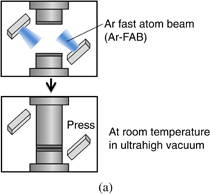
Figure 1 shows the schematic process flow of the SAB and PAB processes. The SAB method started with activating Ge surfaces by Ar-FAB bombardment. When the vacuum condition reached 1 × 10⁻⁵ Pa, the two wafer surfaces were activated simultaneously by the Ar-FAB source for 100–600 s with a voltage of 0.75–1.5 kV and a current of 10–60 mA. The beam incident angle was 45°. The etching rate at several points on the wafer was measured, and the average value for the Ge wafers was approximately 2.7 nm/min for the Ar-FAB source with a voltage of 1.5 kV and a current of 60 mA. Immediately after surface activation, the top wafer was moved down and the two wafers were brought into direct contact under a pressure of 1.2 MPa at room temperature in vacuum without exposing them to ambient pressure. The vacuum exposure time was about 30 s. In the PAB process, Ge wafers were treated by a 200 W O2 plasma created in a reactive ion etcher (RIE) for 60 s to obtain a hydrophilic surface. Then, the wafers were placed in contact in a 75% humidity atmosphere at room temperature and became weakly attached by a hydrogen-bonded water layer. Then, the wafers in contact were annealed at 300 °C for 10 h to obtain a high bonding strength.
Download figure:
Standard image High-resolution image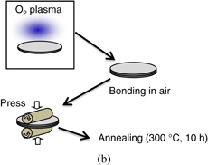
Fig. 1. Schematic process flow of low-temperature wafer bonding. (a) SAB and (b) PAB.
Download figure:
Standard image High-resolution imageAfter bonding, the bonded wafers were inspected for unbonded areas (voids) using a scanning acoustic microscope (SAM). A transducer frequency of 100 MHz with a resolution of approximately 15 µm was used. The bonding energy was evaluated by a razor blade test (crack-opening method).22) The bonding strength was evaluated by tensile and dicing tests.
To characterize the electrical properties of the bonded interface, the I–V characteristics of the bonded samples were measured by the four-point probe technique to eliminate the effects of resistance between the probe and the metal electrodes. A metallization scheme of Cr/Au (50/250 nm) was deposited on the Ge wafers after the bonding experiments. The nonalloyed Cr/Au ohmic contacts were confirmed using circular patterned electrodes based on a circular transmission line model (c-TLM).23) After metal deposition, the bonded Ge wafer pairs were cut into 3 × 3 mm2 pieces for I–V measurements. All measurements were carried out at room temperature.
The microstructure of the bonded interface was observed using a TEM system operated at 300 kV. The chemical composition of the interface was investigated by energy-dispersive X-ray spectroscopy. Secondary ion mass spectroscopy (SIMS) with a 10.0 kV O2+ primary beam was used to characterize doping profiles across the bonded interface (detection area: 30 µm in diameter). In order to minimize depth profile broadening by knock-on effects, SIMS depth profiling was performed by sputtering from the low-concentration region to the high-concentration region.
3. Results and discussion
3.1. Surface roughness
The AFM analysis had a scan area of 1 × 1 µm2. Seven different spots were scanned on each sample to better reflect the surface roughness. The average root-mean-square (rms) roughness was 0.28 ± 0.02 nm for the sample FAB-irradiated with Ar for 600 s, compared with 0.31 ± 0.05 nm for the as-received sample, indicating that the Ar-FAB irradiation for 600 s does not deteriorate the surface roughness. The two-dimensional power spectral density (PSD) function was computed from the AFM images in order to evaluate the typical lateral dimension of the surface features. AFM data were processed by WSxM software.24) Figure 2 shows the two-dimensional PSD of the AFM data. Analysis of the PSD indicates that the number of short-wavelength asperities (high-spatial-frequency region) is increased by Ar-FAB irradiation. On the basis of the theory of elastic deformation and energy gain by bond formation assuming a surface profile having a single sinusoidal waveform, the criterion for direct wafer bonding is given by15)

where Rrms is the rms surface roughness, λ is the wavelength of the surface profile, E is Young's modulus, ν is Poisson's ratio, and WA is the work of adhesion. In the case of bonding to the same material, the work of adhesion becomes WA = 2γ, where γ is the surface energy. Using ν = 0.26,25) E = 103 GPa,25) γ = 1.84 J/m2,26) and λ = 37 and 7.9 nm, deduced from the peaks of the PSD function shown in Fig. 2, the critical roughness was calculated as Rrms ≤ 0.9 nm (λ = 37 nm) and Rrms ≤ 0.41 nm (λ = 7.9 nm). The actual rms roughness of the Ge wafers was 0.28 ± 0.02 nm, which is smooth enough for direct wafer bonding.
Fig. 2. Two-dimensional PSD of AFM data.
Download figure:
Standard image High-resolution image3.2. Surface analysis
Surface contamination on the surface of the Ge wafers before bonding was investigated using XPS. The wide-scan XPS spectra showed C- and O-related signals on the as-received Ge wafers. The peaks of C completely disappeared after Ar-FAB sputtering for 20 s. The Ar-FAB sputtering rate of Ge was 3.6 nm/min. Figure 3 shows the XPS spectra of the Ge 3d and O 1s core levels. The Ge 3d core-level peak at 29 eV is a combination of unresolved 3d3/2 and 3d5/2 peaks. An additional broad peak, shifted by 3.4 eV toward higher binding energies and originating from the native oxide (GeO2), was observed on the surface of the as-received Ge wafers. The peak intensity of GeO2 at 32.4 eV decreased significantly after a short sputtering for 20 s and the intensity of the elemental Ge 3d peak increased concurrently. It is assumed that the native oxide of Ge has a thickness of less than 1.2 nm. The peak intensity of O 1s also decreased significantly after a short sputtering for 20 s and gradually decreased to a minimum after sputtering for 100 s. Since the average etching rate of the Ge wafers at the SAB bonder was approximately 2.7 nm/min, the required Ar-FAB irradiation time was more than 30 s.
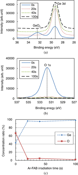
Fig. 3. Depth profile of the composition of Ge surface taken by XPS. (a) Ge 3d core-level spectra, (b) O 1s core-level spectra, and (c) quantification.
Download figure:
Standard image High-resolution image3.3. Bonding strength
Figure 4 shows a SAM image of the bonded 2-in. Ge–Ge wafers. Dark and bright areas in the image represent well-bonded and unbonded regions (such as voids), respectively. The bright areas at the edge of the wafer pair are also not bonded. The SAM image indicates that the entire area was bonded with a few particle-induced voids. The bond energy was examined by the razor blade test. However, the blade could hardly be inserted between the bonded wafers, whereas cracks occurred on one side of the bonded wafers (Fig. 5). The bonding strength was then investigated by the tensile test. The bonded wafers were cut into 10 × 10 mm2 pieces and fixed to the attachments of a pulling test machine with adhesive glue. The tensile test speed was 0.3 mm/min. The obtained tensile strength was above 14 MPa. Figure 6 shows an image of the fractured surfaces after the tensile test. The fracture occurred from the adhesive glue or inside the Ge bulk material. The dicing test was also performed for the bonded wafer, which was diced to 10 × 10 mm2 pieces and then further diced to 0.5 × 0.5 mm2 small pieces. Chip-free dices with smooth edges were observed as shown in Fig. 7. Both the high tensile strength and the perfect dicing indicate the strong bond of the Ge–Ge wafers bonded by SAB at room temperature.
Fig. 4. SAM image of a 2-in. Ge/Ge wafer pair bonded by SAB.
Download figure:
Standard image High-resolution image
Fig. 5. Bonded Ge/Ge wafer pair after bulk fracture in the blade insertion test.
Download figure:
Standard image High-resolution image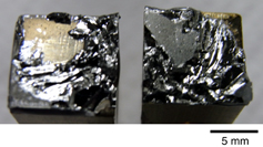
Fig. 6. Fractured surfaces of the Ge/Ge bonded samples after tensile test.
Download figure:
Standard image High-resolution image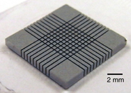
Fig. 7. Photograph of diced chip. A bonded Ge/Ge wafer was diced to 10 × 10 mm2 pieces and then further diced to 0.5 × 0.5 mm2 small pieces.
Download figure:
Standard image High-resolution imageFigure 8 shows the effect of the background vacuum pressure on the bonding energies of Ge/Ge and Si/Si wafers for comparison. The vacuum pressure was measured before Ar-FAB irradiation. The bonding energy of Si/Si wafers strongly depends on the background vacuum pressure compared with that of Ge/Ge wafers. The bonding energy of Si/Si wafers was more than 1.95 J/m2 at 2.5 × 10⁻⁶ Pa, whereas it was only approximately 0.01 J/m2 at 4.5 × 10⁻⁴ Pa. It is considered that the residual gas (mainly H2O) in the bonding chamber reacted with the activated Si surface during vacuum exposure after surface activation. In contrast, the Ge/Ge bonding was so strong that we could not insert the razor blade and the bonding energy of Ge/Ge wafers is considered to be close to the bulk Ge fracture energy (γ = 1.84 J/m2)26) even at a background vacuum pressure of 10−3 Pa. This difference seems to result from the large difference in the sticking probability of H2O. It is known that the sticking probability s is close to one for H2O adsorption on Si(100), while it is several orders of magnitude lower (s = 2 × 10⁻⁴) for Ge(100) at room temperature.27–29) This indicates that it is more difficult for H2O to adsorb on the Ge surface. The estimated background vacuum pressure required to form a monolayer of adsorbed H2O molecules during vacuum exposure is on the order of 10−5 Pa for Si and 10−2 Pa for Ge, as observed in our experiments.
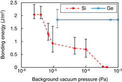
Fig. 8. Effect of background vacuum pressure on bonding energy.
Download figure:
Standard image High-resolution image3.4. Electrical properties of bonded interface
I–V characteristics of the bonded samples are shown in Fig. 9. P-type Ge wafers with the same resistivity of 0.1–0.5 Ω cm were used for the bonding. The samples bonded by PAB showed a resistance (5.9 Ω) much higher than the bulk resistance (0.11–0.55 Ω), whereas the samples bonded by SAB had a resistance almost equal to the bulk resistance [Fig. 9(a)]. To compare the effects of annealing on the I–V characteristics, some of the bonded samples were additionally annealed at 500 °C for 1 h. The samples bonded by PAB with additional annealing showed a reduced resistance (0.22 Ω) and the I–V curve became linear [Fig. 9(b)]. There was no difference between the samples bonded by SAB with and without additional annealing (0.15 Ω). Even with additional annealing, the samples bonded by PAB had a slightly higher resistance than the samples bonded by SAB.

Download figure:
Standard image High-resolution image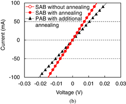
Fig. 9. I–V characteristics of p-Ge/p-Ge bonded interface. (a) Ge/Ge interfaces were prepared by SAB (Ar-FAB: 1.5 kV, 60 mA) and PAB (O2 RIE: 200 W, annealing: 300 °C, 10 h). (b) Bonded samples were additionally annealed at 500 °C for 1 h.
Download figure:
Standard image High-resolution image3.5. Microstructure of bonded interface
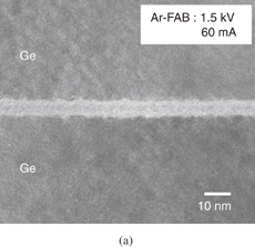
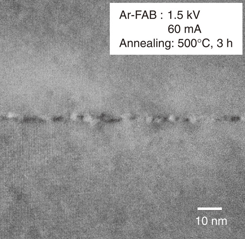
TEM images of the cross-sectional Ge/Ge bonded interface are shown in Figs. 10 and 11. Figure 10 shows TEM images of the interface bonded by SAB at room temperature. The TEM observations showed that direct bonding at the atomic scale was achieved. It was found that the Ge/Ge interface had a disordered amorphous interlayer, which might have been formed by the Ar-FAB irradiation [Fig. 10(b)]. The thickness of the amorphous layer decreased from 8 to 3 nm when the Ar beam energy decreased as shown in Figs. 10 and 11(a). Figure 11(b) shows a TEM image of the interface bonded by oxygen PAB with annealing at 300 °C for 10 h. An interlayer is also observed at the bonded interface. Figures 12 and 13 show EDX spectra of the interfaces prepared by SAB and PAB, respectively. EDX analysis of the interface prepared by the SAB method indicated that the amorphous interlayer was mainly composed of Ge [Fig. 12(a)]. Ge/Ge junctions prepared by the SAB method have advantageous electrical properties due to the oxide-free surfaces. EDX analysis of the interface prepared by the PAB method indicated that the interlayer was mainly composed of Ge and small amounts of O [Fig. 13(a)]. It is assumed that C is a contaminant formed during TEM observation. The existence of a thin oxide layer (GeO2) increases the junction resistance, as shown in Fig. 9, and is not appropriate for applications where low junction resistance is important. Figure 14 shows a TEM image of an interface bonded by SAB at room temperature and annealed at 500 °C for 3 h. Although a change in the measured I–V curve of samples bonded by SAB was not observed after annealing, the nearly continuous amorphous layer disappeared during annealing and the formation of a locally perfect interface was observed. It is considered that the local recrystallization of the thin amorphous layer takes place during annealing. It was reported that the recrystallization of amorphous Ge(111) occurs at approximately 300 °C, which is lower than the temperature of 510 °C for the Si(111) surface.30)
Download figure:
Standard image High-resolution image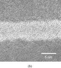
Fig. 10. Cross-sectional TEM images of Ge/Ge interface prepared by SAB at room temperature. (a) Applied voltage to the Ar FAB source: 1.5 kV and (b) enlarged view.
Download figure:
Standard image High-resolution image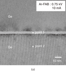
Download figure:
Standard image High-resolution image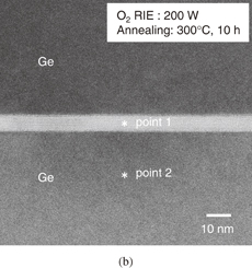
Fig. 11. Cross-sectional TEM images of Ge/Ge interface prepared by (a) SAB (Ar-FAB: 0.75 kV, 10 mA) and (b) PAB (O2 RIE: 200 W, annealing: 300 °C, 10 h).
Download figure:
Standard image High-resolution image
Download figure:
Standard image High-resolution image
Fig. 12. EDX spectra of Ge/Ge interface prepared by SAB. (a) Interlayer (point 1) and (b) bulk region (point 2). The analyzed points are indicated in Fig. 11(a).
Download figure:
Standard image High-resolution image
Download figure:
Standard image High-resolution image
Fig. 13. EDX spectra of Ge/Ge interface prepared by PAB. (a) Interlayer (point 1) and (b) bulk region (point 2). The analyzed points are indicated in Fig. 11(b).
Download figure:
Standard image High-resolution image
Fig. 14. Cross-sectional TEM image of Ge/Ge interface prepared by SAB (Ar-FAB: 1.5 kV, 60 mA) at room temperature after annealing at 500 °C for 3 h.
Download figure:
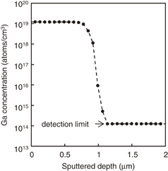
Standard image High-resolution imageFigure 15 shows the depth profile of the Ga concentration across a bonded interface. P-type Ge wafers with doping concentrations of ∼1014 and ∼1019 cm−3 were used for the bonding. Since the SIMS detection limit of Ga in Ge is 1014 atoms/cm3, a Ga doping level of 1014 atoms/cm3 or lower could not be determined accurately. The SIMS analysis indicates a sharp Ga impurity concentration gradient across the bonded interface. This elimination of a broad dopant transition region is a characteristic of room-temperature direct bonding and an advantage over the traditional high-temperature growth process.
Fig. 15. Ga concentration profile measured by SIMS.
Download figure:
Standard image High-resolution image
4. Conclusions
We have demonstrated the room-temperature direct bonding of Ge wafers using Ar beam surface activation. The bonding interface of Ge–Ge wafers was nearly void-free. The bonded wafers were perfectly diced into small pieces and the bonding strength exceeded 14 MPa. The measured I–V curve across the Ge/Ge bonded interface shows the formation of junctions with very low resistance at room temperature. This room-temperature bonding method of Ge wafers is expected to be a promising technique for future infrared detection applications.
Acknowledgment
Part of this study was supported by a Grant-in-Aid for Scientific Research (B) (22360025) from the Japan Society for the Promotion of Science (JSPS).