
Abstract
We proposed and fabricated a current-driven phase-change optical gate switch using a Ge2Sb2Te5 (GST225) thin film, an indium–tin-oxide (ITO) heater, and a Si waveguide. Microfabrication technology compatible with CMOS fabrication was used for the fabrication of the Si waveguide. The repetitive phase changing of GST225 was obtained by injecting a current pulse into the ITO heater beneath the GST225 thin film. The switching operation was observed by injecting a 100-ns current pulse of 20 mA into the ITO heater. The average extinction ratio over the wavelength range of 1,525 to 1,625 nm was 1.2 dB.
Export citation and abstract BibTeX RIS

Content from this work may be used under the terms of the Creative Commons Attribution 4.0 license. Any further distribution of this work must maintain attribution to the author(s) and the title of the work, journal citation and DOI.
Recently, high-performance optical switches (particularly large-scale integrated ones with a low power consumption, broad band, and small size) have been in demand for optical network nodes in order to meet the increasing demand for networks. With this in mind, we focused on the phase-change material (PCM) to be used in a waveguide-type optical switch.1–3) PCMs have been utilized for optical data storage (CDs, DVDs, Blu-ray, etc.)4,5) and solid-state memory called phase-change random-access memory.6,7) Additionally, photonic memory using PCM and SiN waveguides was reported.8,9) The switching time for the phase change between the amorphous and crystalline states is less than several hundred nanoseconds. The physical properties of PCMs vary significantly.10–12) For example, the refractive index changes by tens of percent, and the electrical resistance changes by over three orders of magnitude. The switch can be small because of the large refractive index change of PCM. For example, an optical switch based on the electro-optic effect or thermo-optic effect requires a switch length of >100 µm,13–15) while a phase-change switch can be as small as several micrometers. No external energy is required to maintain the state of the PCM because both the amorphous and crystalline states are stable around room temperature. By utilizing these characteristics and combining them with Si waveguides, fast-operable, ultrasmall, and nonvolatile optical switches can be realized. Phase-change optical gate switches with >1,000 repetitive switching operations and Mach–Zehnder interferometer-based wavelength selective switches using a PCM have already been realized.16–18) However, an electrically controllable switch is needed in order to realize multiple connections and large-scale integration.19,20) The heater must be placed in close proximity to the waveguide core and be such that the light loss from the waveguide is low. Thus, we chose indium–tin-oxide (ITO) instead of metallic heaters such as Pt or TiN. A report of a PCM-based display using ITO electrodes by Peiman Hosseini et al. motivated us to choose this material.21)
In this study, a current-driven phase-change optical gate switch using an ITO heater was proposed and fabricated, and the switching operation was demonstrated.
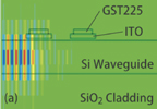
Figure 1 shows a schematic of the proposed optical switch. An ITO heater and a PCM thin film were placed above a Si waveguide. An ITO heater was placed under the PCM to reduce fabrication errors. Ge2Sb2Te5 (GST225) was used as the PCM. The Si waveguide was a single-mode waveguide with a width of 450 nm and a height of 220 nm, but the part for the switch was designed as a multi-mode waveguide with a width of 2 µm to ensure that the GST225 fit within its boundaries. If higher-precision lithography, such as a liquid-immersion ArF exposure, is used, a wide waveguide is not always necessary. Both sides of the ITO film were connected to Au electrodes. SiO2 over-cladding and the GST225 were deposited on the ITO heater. The switch had two phase-change regions with a 1.5 × 1.5 µm2 GST225 patch in order to compare the switching characteristics of the current-driven-type switch with those of the all-optical-type switch, which was controlled by an optical pulse with a beam spot diameter of approximately 1.5 µm.

Fig. 1. Structure of the current-driven phase-change optical gate switch using ITO heaters. (a) Top view of the switch. (b) Cross-sectional view of the switch.
Download figure:
Standard image High-resolution imageAfter deciding the switch structure, we performed a light-propagation simulation using the finite-difference time-domain (FDTD) method in order to determine the switch design parameters. For example, Fig. 2 shows an image of the operation of the phase-change optical gate switch in the simulation. The complex refractive index at a wavelength of 1,550 nm is shown in Table I. The complex refractive index of the ITO at 1,550 nm was measured via ellipsometry, and the other indices were previously measured.16) In the simulation, the transverse-electric (TE) mode signal light of 1,550 nm was input from the left-hand side and propagated through the Si waveguide, as shown in Fig. 2. When the PCM was is in the amorphous state, its refractive index is close to that of Si, and its absorption is small; thus, light propagating in the waveguide is not greatly affected by the PCM thin film. On the other hand, the crystalline state has a high refractive index and strong light absorption; thus, the light is absorbed.
Download figure:
Standard image High-resolution image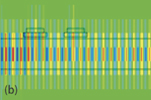
Fig. 2. Light propagation in the region of the switch. (a) GST225 is in the crystalline state (switch state is OFF). (b) GST225 is in the amorphous state (switch state is ON).
Download figure:
Standard image High-resolution imageTable I. Complex refractive index at a wavelength of 1,550 nm.16)
| Material | Refractive index | Extinction coefficient |
|---|---|---|
| Si | 3.48 | 0.00 |
| SiO2 | 1.46 | 0.00 |
| GST225 (amorphous) | 4.39 | 0.16 |
| GST225 (crystalline) | 7.25 | 1.55 |
| ITO | 1.84 | 0.15 |
Table II shows the optimized design parameters for achieving an extinction ratio of 30 dB with the proposed structure (Fig. 1) and the physical properties presented in Table I. The extinction ratio of the switch is mainly determined by the size of the GST225 patch and the thickness of the ITO film. The thickness of the GST225 patch was set to be 0.03 µm for rapid heating and cooling. The width and the length of the GST225 patch and the thickness of the ITO film were optimized to reduce the switching energy by keeping the extinction ratio above 30 dB. Thermal analysis was performed via the finite-element method.
Table II. Size of the ITO heater, GST225 patch, and Au pads (units: µm).
| Width | Length | Thickness | |
|---|---|---|---|
| ITO heater | 2.25 | 3 | 0.03 |
| GST225 | 1.5 | 1.5 | 0.03 |
| Au pad | 60 | 60 | 0.2 |
The width of the ITO heater was 1.5 times that of the GST225 patch in order to ensure uniform heating. The length of the ITO film was set to 3 µm so that the Au electrodes were not above the waveguide. According to the results of the FDTD simulation using these parameter values, the transmission in the ON and OFF states is −2.2 and −32.6 dB, respectively, and the extinction ratio is theoretically estimated to be 30.4 dB.
Before the switch fabrication, we fabricated a test device for confirming the phase change with the ITO heater. The structure of this device is shown in Fig. 3. The ITO and GST225 films were deposited via sputtering, and the SiO2 was deposited via atomic layer deposition. Electron-beam vapor deposition was used for depositing Au. The GST225 patch and the Au electrodes were formed via liftoff processes, and the ITO heater was formed via wet etching. For switching, an under-layer ITO thin film was used as a heater. With this device, the change in resistance with the phase change was measured using the upper and lower ITO layers as electrodes. In addition, the change in color with the phase change was observed because ITO is a transparent material. The typical pattern size of the ITO heater and GST225 patch was set to a value similar to that shown in Table II.

Download figure:
Standard image High-resolution image
Fig. 3. Structure of the test device. (a) Top view of the device. (b) Cross-sectional view.
Download figure:
Standard image High-resolution imageFigure 4 shows a scanning electron microscopy (SEM) image of the fabricated test device, which indicates that the GST225 was correctly deposited on the cross part of the ITO films. The GST225 patch and upper ITO layers were patterned via liftoff processes, and each had some edge roughness, but the size was fabricated as designed in each case.

Fig. 4. SEM Image of the test device.
Download figure:
Standard image High-resolution imageTo induce phase changes in the GST225, a 100-ns-wide current pulse of 12 mA was used for amorphization, and a 100-ms-wide pulse of 6.5 mA was used for crystallization. This is because rapid heating over the melting point and rapid cooling are needed for amorphization, and relatively long heating above the crystallization temperature below the melting point is needed for crystallization. In this experiment, repeated changes in the reflection ratio and the resistance of the GST225 associated with the phase change were observed. The resistance of the ITO film beneath the GST225 was approximately 1 kΩ; thus, the energy consumption for amorphization and crystallization was calculated to be 14.4 and 4.2 mJ, respectively. In this experiment, the energy consumption of crystallization was larger than that of amorphization because the injection pulse for crystallization is longer than that for amorphization. Then, the GST225 was heated above its melting point of 650 °C for amorphization and above the crystallization temperature of 250 °C for crystallization. Figures 5(a) and 5(b) show optical microscope images of the GST225 patch in the amorphous and crystalline states, respectively. The crystalline state appears bright because it has a high refractive index and a high reflection ratio, while the amorphous state, which has low refractive index, appears dark. The color-invariant part around the dark GST225 patch is a shadow formed by the rough edge of the GST225. The change in resistance with the phase change in the GST225 is shown in Fig. 6, indicating that repetitive resistance changes of 2 or 3 orders of magnitude were induced by injecting current pulses. The resistance of the amorphous states varied by approximately one order of magnitude. However, almost all of the GST225 is considered to have been phase-changed because the resistance ratio of the amorphous state to the crystalline state are very large. Therefore, the total absorption in the amorphous states may be almost constant for the optical switch. The above demonstrates that the repetitive phase change of the GST225 using the ITO heater was accomplished.
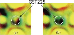
Fig. 5. Repetetive changes in the reflectance of the GST225 patch (indicated by white broken circular lines) were observed. (a) Photograph of the amorphous state in the GST225 patch. (b) Crystalline state.
Download figure:
Standard image High-resolution image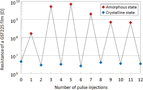
Fig. 6. Repetitive resistance change with the phase change of the GST225.
Download figure:
Standard image High-resolution imagePost-processing to form the GST225 patch and the heater was performed on diced Si waveguide chips from a 12-in. wafer. These chips were fabricated by using a CMOS pilot line at Advanced Industrial Science and Technology (AIST). The fabrication processes were the same as those for the test device. In this fabrication process, the chip was annealed above the crystalline temperature; thus, the GST225 in the fabricated device was completely crystallized. An SEM image of the fabricated device is shown in Fig. 7, which shows that the GST225 patch is correctly positioned on the Si waveguide, extending longitudinally. The white part around the GST225 patch is the rough edge generated by the liftoff process.
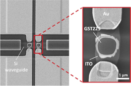
Fig. 7. SEM images of the phase-change gate switch.
Download figure:
Standard image High-resolution imageFigure 8 shows the experimental setup used for measurements of the device characteristics. A wavelength-tunable laser source was used to measure the wavelength dependence of the switch. The polarization of the input light was adjusted to the TE mode of the waveguide, and the wavelength range was 1,525 to 1,625 nm. Light propagated through a polarization-maintaining fiber (PMF) and was then focused and input into the chip using a lens fiber fixed to the end of the PMF. The output light propagated through a similar optical path and was detected by a photodiode. On the top of the chip, the current pulse generated by a pulse pattern generator was injected into the electrodes, and the ITO was heated in order to operate the switch.
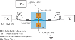
Fig. 8. Experimental setup for the switching operation.
Download figure:
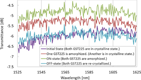
Standard image High-resolution imageFigure 9 shows the optical transmission characteristics of the phase-change optical gate switch measured over the wavelength range of 1,525 to 1,625 nm. This graph does not include the 11.4 dB of coupling loss between the lens fiber and the Si waveguide. The ripple in the waveform was due to the interferometer formed by reflections at the both end facets of the chip. A 100-ns-wide current pulse of 20 mA was used for amorphization, and a 100-ms-wide pulse of 12 mA was used for crystallization. The resistance of the ITO heater was approximately 500 Ω; thus, the energy consumption was calculated to be 20 nJ for amorphization and 7.2 mJ for crystallization, respectively. In the initial state, the GST225 was crystalline, and the average transmission was −6.0 dB. Injecting a 100-ns-wide current pulse of 20 mA into one ITO heater caused amorphization, and the average transmission changed to −5.3 dB. Then, the same pulse was injected into another heater, the transmission changed to −4.8 dB. Finally, a 100-ms-wide current pulse of 12 mA was injected into both heaters for crystallization, and the transmission returned to −6.0 dB, which is close to that of the initial state. This experimental result implies that the proposed switch can operate over a band wider than 100 nm and centered at 1,550 nm.
Fig. 9. Optical transmission characteristics of the phase-change optical gate switch.
Download figure:
Standard image High-resolution image
The measured extinction ratio of 1.2 dB is markedly different from the simulated value of 30.4 dB. In contrast, according to the FDTD simulations assuming the extinction ratio of 1.2 dB, the GST225 film thickness is estimated to be approximately 9 nm. To determine the cause of the low extinction ratio, a cross-section of the switch was examined using a focused ion beam apparatus, revealing that the GST225 film was thinner than assumed. This was because of incomplete sputtering caused by a thick photoresist. Thus, by improving the fabrication process, a switch with a larger extinction ratio can be realized.
In conclusion, we successfully fabricated a current-driven phase-change optical gate switch using an ITO heater and demonstrated switching operations. We confirmed the repetitive operation of the switching part was over 10 times by both the measurement of the resistance and the color change of the GST225 film. The device was fabricated and operated on an actual Si waveguide. We determined that the average extinction ratio was 1.2 dB over the wavelength range of 1,525 to 1,625 nm. We will improve the device and realize an ultrasmall and low-power consumption optical switch.
Acknowledgments
This work was conducted at the AIST Nano-Processing Facility and supported by the "Nanotechnology Platform Program" of the Ministry of Education, Culture, Sports, Science and Technology, Japan (MEXT). Authors are grateful to Professor Hideo Hosono of Tokyo Institute of Technology for his valuable suggestions on ITO.